EP0106637A1 - Eléments optiques transparents aux rayons infrarouges - Google Patents
Eléments optiques transparents aux rayons infrarouges Download PDFInfo
- Publication number
- EP0106637A1 EP0106637A1 EP83306057A EP83306057A EP0106637A1 EP 0106637 A1 EP0106637 A1 EP 0106637A1 EP 83306057 A EP83306057 A EP 83306057A EP 83306057 A EP83306057 A EP 83306057A EP 0106637 A1 EP0106637 A1 EP 0106637A1
- Authority
- EP
- European Patent Office
- Prior art keywords
- coating
- substrate
- chamber
- cathode
- infra red
- Prior art date
- Legal status (The legal status is an assumption and is not a legal conclusion. Google has not performed a legal analysis and makes no representation as to the accuracy of the status listed.)
- Granted
Links
Images
Classifications
-
- G—PHYSICS
- G02—OPTICS
- G02B—OPTICAL ELEMENTS, SYSTEMS OR APPARATUS
- G02B1/00—Optical elements characterised by the material of which they are made; Optical coatings for optical elements
- G02B1/10—Optical coatings produced by application to, or surface treatment of, optical elements
- G02B1/12—Optical coatings produced by application to, or surface treatment of, optical elements by surface treatment, e.g. by irradiation
-
- C—CHEMISTRY; METALLURGY
- C23—COATING METALLIC MATERIAL; COATING MATERIAL WITH METALLIC MATERIAL; CHEMICAL SURFACE TREATMENT; DIFFUSION TREATMENT OF METALLIC MATERIAL; COATING BY VACUUM EVAPORATION, BY SPUTTERING, BY ION IMPLANTATION OR BY CHEMICAL VAPOUR DEPOSITION, IN GENERAL; INHIBITING CORROSION OF METALLIC MATERIAL OR INCRUSTATION IN GENERAL
- C23C—COATING METALLIC MATERIAL; COATING MATERIAL WITH METALLIC MATERIAL; SURFACE TREATMENT OF METALLIC MATERIAL BY DIFFUSION INTO THE SURFACE, BY CHEMICAL CONVERSION OR SUBSTITUTION; COATING BY VACUUM EVAPORATION, BY SPUTTERING, BY ION IMPLANTATION OR BY CHEMICAL VAPOUR DEPOSITION, IN GENERAL
- C23C16/00—Chemical coating by decomposition of gaseous compounds, without leaving reaction products of surface material in the coating, i.e. chemical vapour deposition [CVD] processes
- C23C16/02—Pretreatment of the material to be coated
- C23C16/0272—Deposition of sub-layers, e.g. to promote the adhesion of the main coating
-
- C—CHEMISTRY; METALLURGY
- C23—COATING METALLIC MATERIAL; COATING MATERIAL WITH METALLIC MATERIAL; CHEMICAL SURFACE TREATMENT; DIFFUSION TREATMENT OF METALLIC MATERIAL; COATING BY VACUUM EVAPORATION, BY SPUTTERING, BY ION IMPLANTATION OR BY CHEMICAL VAPOUR DEPOSITION, IN GENERAL; INHIBITING CORROSION OF METALLIC MATERIAL OR INCRUSTATION IN GENERAL
- C23C—COATING METALLIC MATERIAL; COATING MATERIAL WITH METALLIC MATERIAL; SURFACE TREATMENT OF METALLIC MATERIAL BY DIFFUSION INTO THE SURFACE, BY CHEMICAL CONVERSION OR SUBSTITUTION; COATING BY VACUUM EVAPORATION, BY SPUTTERING, BY ION IMPLANTATION OR BY CHEMICAL VAPOUR DEPOSITION, IN GENERAL
- C23C16/00—Chemical coating by decomposition of gaseous compounds, without leaving reaction products of surface material in the coating, i.e. chemical vapour deposition [CVD] processes
- C23C16/02—Pretreatment of the material to be coated
- C23C16/0272—Deposition of sub-layers, e.g. to promote the adhesion of the main coating
- C23C16/029—Graded interfaces
-
- C—CHEMISTRY; METALLURGY
- C23—COATING METALLIC MATERIAL; COATING MATERIAL WITH METALLIC MATERIAL; CHEMICAL SURFACE TREATMENT; DIFFUSION TREATMENT OF METALLIC MATERIAL; COATING BY VACUUM EVAPORATION, BY SPUTTERING, BY ION IMPLANTATION OR BY CHEMICAL VAPOUR DEPOSITION, IN GENERAL; INHIBITING CORROSION OF METALLIC MATERIAL OR INCRUSTATION IN GENERAL
- C23C—COATING METALLIC MATERIAL; COATING MATERIAL WITH METALLIC MATERIAL; SURFACE TREATMENT OF METALLIC MATERIAL BY DIFFUSION INTO THE SURFACE, BY CHEMICAL CONVERSION OR SUBSTITUTION; COATING BY VACUUM EVAPORATION, BY SPUTTERING, BY ION IMPLANTATION OR BY CHEMICAL VAPOUR DEPOSITION, IN GENERAL
- C23C16/00—Chemical coating by decomposition of gaseous compounds, without leaving reaction products of surface material in the coating, i.e. chemical vapour deposition [CVD] processes
- C23C16/22—Chemical coating by decomposition of gaseous compounds, without leaving reaction products of surface material in the coating, i.e. chemical vapour deposition [CVD] processes characterised by the deposition of inorganic material, other than metallic material
- C23C16/30—Deposition of compounds, mixtures or solid solutions, e.g. borides, carbides, nitrides
- C23C16/32—Carbides
-
- C—CHEMISTRY; METALLURGY
- C23—COATING METALLIC MATERIAL; COATING MATERIAL WITH METALLIC MATERIAL; CHEMICAL SURFACE TREATMENT; DIFFUSION TREATMENT OF METALLIC MATERIAL; COATING BY VACUUM EVAPORATION, BY SPUTTERING, BY ION IMPLANTATION OR BY CHEMICAL VAPOUR DEPOSITION, IN GENERAL; INHIBITING CORROSION OF METALLIC MATERIAL OR INCRUSTATION IN GENERAL
- C23C—COATING METALLIC MATERIAL; COATING MATERIAL WITH METALLIC MATERIAL; SURFACE TREATMENT OF METALLIC MATERIAL BY DIFFUSION INTO THE SURFACE, BY CHEMICAL CONVERSION OR SUBSTITUTION; COATING BY VACUUM EVAPORATION, BY SPUTTERING, BY ION IMPLANTATION OR BY CHEMICAL VAPOUR DEPOSITION, IN GENERAL
- C23C16/00—Chemical coating by decomposition of gaseous compounds, without leaving reaction products of surface material in the coating, i.e. chemical vapour deposition [CVD] processes
- C23C16/22—Chemical coating by decomposition of gaseous compounds, without leaving reaction products of surface material in the coating, i.e. chemical vapour deposition [CVD] processes characterised by the deposition of inorganic material, other than metallic material
- C23C16/30—Deposition of compounds, mixtures or solid solutions, e.g. borides, carbides, nitrides
- C23C16/32—Carbides
- C23C16/325—Silicon carbide
Definitions
- the invention concerns a method and apparatus for depositing coatings in a glow discharge plasma.
- Coating may be of hard carbon, silicon, germanium or other suitable materials capable of being deposited from suitable plasma.
- Carbon coatings are useful on for example germanium lenses used in infra red thermal imagers since the cargon coatings are very hard, wear-resistant and substantially transparent to infra-red radiation. Both silicon and germanium are transparent to infra red and are useful in various infra red equipments.
- a substrate may be suspended above a cathode target of the coating material in a vacuum.
- Argon ions are caused to strike the target thereby knocking off small particles of the target material which adhere to the substrate.
- Such a technique is known as sputtering.
- Carbon can be sputtered but the deposition rate is low and the coating may be graphitic.
- Coatings may be grown in a plasma.
- a substrate may be used as a cathode in a D.C. or A.C. excited hydrocarbon plasma.
- Carbon ions are attracted to strike the substrate and form a carbon layer which for appropriate temperature and pressure conditions, is diamond-like.
- a disadvantage with the prior art flow discharge deposition is that in order to achieve reasonable deposition rates high potentials have to be applied or developed at the cathode, so that the substrate is subjected to high energy incident particles. This tends to affect the stress in the coating and increases the back sputtering rate. In some cases this prevents deposition of a layer at all.
- a method of depositing coatings containing carbon and another element comprises the steps of providing a plasma containing the materials to be deposited as a coating in a chamber having a cathode structure, arranging a substrate to be coated on the cathode, and maintaining the substrate at an elevated temperature during growth.
- the elevated temperature is high enough, e.g. above about 400°C, to drive out the required amount of hydrogen.
- a typical temperature is about 530 0 C although most hydrogen is driven out below this e.g. at about 500°C.
- apparatus for depositing a coating on a substrate comprises a vacuum tight chamber, a pump for maintaining a vacuum within the chamber, means for supplying a mixture of at least two gases into the chamber, an. anode and a cathode structure within the chamber, a cathode heater, a power supply for providing a glow discharge in the chamber adjacent the cathode, the arrangement being such that a plasma of at least two gaseous materials is established in the chamber so that ions of the material deposit on the substrate arranged on the cathode to form a coating.
- one of the gas supplies may be replaced by a molecular beam oven or an ion beam source etc to provide one of the materials in the plasma.
- This oven or source may be mounted in the chamber and direct its contents into the region around the cathode.
- a lens or window is provided with a coating by the above method.
- the coating may be a thin coating on the surface of a component such as a lens or window or may be grown as a thick layer self supporting after removal of the substrate.
- the coating may be of Ge x C 1-x , Si x C 1-x where 0 ⁇ x ⁇ 1.
- Small amounts of Ge, Si give a hard carbon coating that is relatively strain free due to the inclusion of Ge, Si. Thus quite thick strain free layers may be grown. Also the high temperature of growth results in little if any H 2 within the layer. This results in a coating which absorbs little infra red light.
- hard carbon layers grown by the prior art methods .contain hydrogen and interstitial carbon which gives rise to black absorbing layers and highly strained layers.
- the glow discharge may be provided by D.C. or A.C. at any suitable frequency.
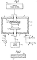
- the apparatus of Figure 1 comprises a vacuum tight container 1 formed by an annular wall 2 and earthed top and bottom plates 3, 4 respectively.
- a pump 5 is connected through an exhaust pipe 6 and valve 7 to the chamber 1.
- Gas supplies of argon, germane and a hydrocarbon gas such as butane are fed into the chamber via inlet pipes 8, 9, 10, 11 and valves 12, 13, 14, 15.
- a cathode structure 16 is supported inside the chamber 1 and electrically insulated from the bottom plate 4 by a sleeve 17. Inside the cathode structure is a heater 18 for heating a substrate 19 arranged on the cathode 16. Cathode temperature is controlled by a heater control 20 which also supplies power to the heater 18.
- a power supply 21 feeds electrical power to the cathode 16. This power may be D.C., or A.C. via a blocking capacitor 22. Alternatively an A.C. coil may surround the chamber 1 and induce a plasma within the chamber.
- a germanium lens Figure 2 may be coated with a layer of hard carbon as follows.
- the lens 19 is mounted on the cathode 16 with the surface 22 to be coated uppermost.
- the chamber 1 is evacuated by the pump 5 to less than 10- 5 Torr. to remove contaminants.
- Argon gas is admitted through the valve 13 and the chamber pressure kept at about 10 2 Torr. on an air calibrated gauge.
- a plasma is generated in argon by energising the cathode 16 from the power supply 21. This provides an argon ion bombardment of the surface 22 to clean it prior to coating. About 2 minutes cleaning is usually adequate.
- the cathode heater 18 is operated to raise the lens 19 temperature to above about 500 typically 530°C and maintain it at this value during growth of the coating.
- the argon is removed by the pump 5 and a mixture of germane (GeH 4 ) and butane (CH 4 ) admitted via the inlet pipe 8, 10, 11 and valves 12, 14, 15. Pressure is maintained at around 0.7 to 1.10 -2 Torr.
- A.C. power typically 1 kvolt at 13 MHz and 200 watts power level is applied to create a plasma. Positively charged ions of C, and of Ge strike and remain on the lens surface gradually building up a layer 23 of hard carbon with small amounts of Ge included.
- the layer thickness is time and composition dependent and is selected for optical properties (anti-reflection) and required durability.
- Typical layer thickness is 1 to 10 ⁇ m. The discharge is stopped when the required thickness is grown and the substrate allowed to cool.
- the substrate 19 may be rotated during growth.
- the proportion of Ge in the C varies with the proportions of germane and butane gas admitted. For a hard carbon layer only small amounts of Ge are needed to provide a transparent carbon layer of extreme durability and hardness approaching that of diamond.
- the high substrate temperature prevents the inclusion of H 2 within the coating.
- An advantage of Ge within the coating is the good bond achieved by the coating direct with the bulk Ge lens. Thus for some applications no bonding layers are needed.
- the coating composition may vary within the thickness of the coating by adjusting the germane:butane ratio.
- the value of x in the coating composition Ge x C 1-x is variable between 0 and 1, although the coating may not be homogeneous on a microscopic scale.
- the initial deposits may have an x value around 1 to give a good bonding; subsequent depositions may have an x value approaching zero to give a very hard surface.
- Substrates other than germanium may be coated.
- ZnS, ZnSe to give an infra red transparent lens or window with a hard wear resistant outer surface.
- Coatings of silicon carbide Si x C l-x (0 ⁇ x ⁇ 1) may also be grown as above but using silane instead of germane. Regular and irregular objects may be coated. For example cutting tool tips may be given a hard wear resistant coating. Also circular cross section articles such as glass fibres may be coated using a shaped cathode as described in G.B. Patent Application No. 2,099,212 A. This cathode may take the form of a flat strip wound into an open spiral surrounding the fibre which is slowly drawn through. Alternatively the cathqde may be segments arranged along a helix, or a perforated tube.
- the plasma may be generated by D.C. power typically at -2 kvolt. Both conducting and insulating substrates may be coated. Insulating substrates may need a cathode structure of large area compared to substrate area.
Landscapes
- Chemical & Material Sciences (AREA)
- Mechanical Engineering (AREA)
- Metallurgy (AREA)
- Organic Chemistry (AREA)
- General Chemical & Material Sciences (AREA)
- Chemical Kinetics & Catalysis (AREA)
- Engineering & Computer Science (AREA)
- Materials Engineering (AREA)
- Inorganic Chemistry (AREA)
- Physics & Mathematics (AREA)
- Optics & Photonics (AREA)
- General Physics & Mathematics (AREA)
- Surface Treatment Of Optical Elements (AREA)
- Carbon And Carbon Compounds (AREA)
- Chemical Vapour Deposition (AREA)
- Crystals, And After-Treatments Of Crystals (AREA)
Applications Claiming Priority (2)
| Application Number | Priority Date | Filing Date | Title |
|---|---|---|---|
| GB8229124 | 1982-10-12 | ||
| GB8229124 | 1982-10-12 |
Publications (2)
| Publication Number | Publication Date |
|---|---|
| EP0106637A1 true EP0106637A1 (fr) | 1984-04-25 |
| EP0106637B1 EP0106637B1 (fr) | 1988-02-17 |
Family
ID=10533549
Family Applications (1)
| Application Number | Title | Priority Date | Filing Date |
|---|---|---|---|
| EP83306057A Expired EP0106637B1 (fr) | 1982-10-12 | 1983-10-06 | Eléments optiques transparents aux rayons infrarouges |
Country Status (4)
| Country | Link |
|---|---|
| EP (1) | EP0106637B1 (fr) |
| JP (1) | JPS59214003A (fr) |
| DE (1) | DE3375700D1 (fr) |
| GB (1) | GB2129833B (fr) |
Cited By (9)
| Publication number | Priority date | Publication date | Assignee | Title |
|---|---|---|---|---|
| GB2162207A (en) * | 1984-07-26 | 1986-01-29 | Japan Res Dev Corp | Semiconductor crystal growth apparatus |
| DE3615627A1 (de) * | 1985-05-11 | 1986-11-13 | Barr & Stroud Ltd., Glasgow, Schottland/Scotland | Verfahren und vorrichtung zum beschichten optischer bauelemente |
| EP0209972A1 (fr) * | 1985-06-05 | 1987-01-28 | Plessey Overseas Limited | Procédé pour le dépôt d'un carbure de germanium hydrogéné |
| EP0210724A1 (fr) * | 1985-06-05 | 1987-02-04 | Plessey Overseas Limited | Procédé pour le dépôt d'un carbure de germanium |
| WO1988004333A1 (fr) * | 1986-12-10 | 1988-06-16 | The British Petroleum Company P.L.C. | Production de carbure de silicium |
| EP0224360B1 (fr) * | 1985-11-12 | 1992-04-08 | Semiconductor Energy Laboratory Co., Ltd. | Procédé de fabrication d'un dispositif à semi-conducteur |
| US6784033B1 (en) | 1984-02-15 | 2004-08-31 | Semiconductor Energy Laboratory Co., Ltd. | Method for the manufacture of an insulated gate field effect semiconductor device |
| US8366830B2 (en) | 2003-03-04 | 2013-02-05 | Cree, Inc. | Susceptor apparatus for inverted type MOCVD reactor |
| US8372204B2 (en) * | 2002-05-13 | 2013-02-12 | Cree, Inc. | Susceptor for MOCVD reactor |
Families Citing this family (9)
| Publication number | Priority date | Publication date | Assignee | Title |
|---|---|---|---|---|
| US5780313A (en) | 1985-02-14 | 1998-07-14 | Semiconductor Energy Laboratory Co., Ltd. | Method of fabricating semiconductor device |
| GB2291888B (en) * | 1984-06-08 | 1996-06-26 | Barr & Stroud Ltd | Optical coating |
| JPH067202B2 (ja) * | 1985-08-03 | 1994-01-26 | 日本合成ゴム株式会社 | 光学製品の製造方法 |
| GB2185758B (en) * | 1985-12-28 | 1990-09-05 | Canon Kk | Method for forming deposited film |
| GB8713922D0 (en) * | 1987-06-15 | 1994-06-22 | Secr Defence | Infra red transparent windows |
| GB8801366D0 (en) * | 1988-01-21 | 1988-02-17 | Secr Defence | Infra red transparent materials |
| DE3832692A1 (de) * | 1988-09-27 | 1990-03-29 | Leybold Ag | Dichtungselement mit einem absperrkoerper aus einem metallischen oder nichtmetallischen werkstoff und verfahren zum auftragen von hartstoffschichten auf den absperrkoerper |
| IT1227877B (it) * | 1988-11-25 | 1991-05-14 | Eniricerche S P A Agip S P A | Procedimento per la deposizione via plasma di strati multipli dimate riale amorfo a composizione variabile |
| JP6046860B2 (ja) * | 2014-03-13 | 2016-12-21 | 富士フイルム株式会社 | 光学部品,赤外線カメラおよび光学部品の製造方法 |
Citations (8)
| Publication number | Priority date | Publication date | Assignee | Title |
|---|---|---|---|---|
| US4127659A (en) * | 1976-01-02 | 1978-11-28 | Avco Corporation | Silicon carbide filaments and method |
| GB2047877A (en) * | 1979-03-26 | 1980-12-03 | Secr Defence | Solar heating panels |
| EP0030638A1 (fr) * | 1979-12-12 | 1981-06-24 | International Business Machines Corporation | Procédé pour le dépôt de couches très minces contenant du silicium ou du germanium |
| GB2067304A (en) * | 1979-11-20 | 1981-07-22 | Nat Res Dev | Infra red reflectors |
| GB2069008A (en) * | 1980-01-16 | 1981-08-19 | Secr Defence | Coating in a glow discharge |
| GB2081695A (en) * | 1980-07-30 | 1982-02-24 | Avco Corp | Surface treatment for carbon |
| GB2082562A (en) * | 1980-08-21 | 1982-03-10 | Secr Defence | Coating germanium or silica with carbon |
| GB2083841A (en) * | 1980-08-21 | 1982-03-31 | Secr Defence | Glow discharge coating |
Family Cites Families (3)
| Publication number | Priority date | Publication date | Assignee | Title |
|---|---|---|---|---|
| US3424661A (en) * | 1966-09-01 | 1969-01-28 | Bell Telephone Labor Inc | Method of conducting chemical reactions in a glow discharge |
| JPS5353263A (en) * | 1976-10-26 | 1978-05-15 | Toshiba Corp | Manufacture of semiconductor element |
| EP0048542B2 (fr) * | 1980-08-21 | 1993-03-31 | National Research Development Corporation | Revêtement de matériau semi-conducteur transparent au rayonnement infra-rouge |
-
1983
- 1983-10-06 DE DE8383306057T patent/DE3375700D1/de not_active Expired
- 1983-10-06 EP EP83306057A patent/EP0106637B1/fr not_active Expired
- 1983-10-10 GB GB08327061A patent/GB2129833B/en not_active Expired
- 1983-10-12 JP JP58189414A patent/JPS59214003A/ja active Granted
Patent Citations (9)
| Publication number | Priority date | Publication date | Assignee | Title |
|---|---|---|---|---|
| US4127659A (en) * | 1976-01-02 | 1978-11-28 | Avco Corporation | Silicon carbide filaments and method |
| GB1560110A (en) * | 1976-01-02 | 1980-01-30 | Avco Corp | Silicon carbide coated filaments and ribbons |
| GB2047877A (en) * | 1979-03-26 | 1980-12-03 | Secr Defence | Solar heating panels |
| GB2067304A (en) * | 1979-11-20 | 1981-07-22 | Nat Res Dev | Infra red reflectors |
| EP0030638A1 (fr) * | 1979-12-12 | 1981-06-24 | International Business Machines Corporation | Procédé pour le dépôt de couches très minces contenant du silicium ou du germanium |
| GB2069008A (en) * | 1980-01-16 | 1981-08-19 | Secr Defence | Coating in a glow discharge |
| GB2081695A (en) * | 1980-07-30 | 1982-02-24 | Avco Corp | Surface treatment for carbon |
| GB2082562A (en) * | 1980-08-21 | 1982-03-10 | Secr Defence | Coating germanium or silica with carbon |
| GB2083841A (en) * | 1980-08-21 | 1982-03-31 | Secr Defence | Glow discharge coating |
Non-Patent Citations (2)
| Title |
|---|
| PATENT ABSTRACTS OF JAPAN, unexamined applications, C field, vol. 6, no. 261, December 21, 1982 THE PATENT OFFICE JAPANESE GOVERNMENT, page 150 C 141 * JP-a 57 155 365 (MITSUBISHI KINZOKU K.K.) 25-09-1983* * |
| PATENT ABSTRACTS OF JAPAN, unexamined applications, C section, vol. 3, no. 19, February 17, 1979 THE PATENT OFFICE JAPANESE GOVERNMENT, page 142 C 37 * Jp-a 53 144 891 (NIPPON DENSHIN DENWA KOSHA) * * |
Cited By (12)
| Publication number | Priority date | Publication date | Assignee | Title |
|---|---|---|---|---|
| US6784033B1 (en) | 1984-02-15 | 2004-08-31 | Semiconductor Energy Laboratory Co., Ltd. | Method for the manufacture of an insulated gate field effect semiconductor device |
| GB2162207A (en) * | 1984-07-26 | 1986-01-29 | Japan Res Dev Corp | Semiconductor crystal growth apparatus |
| GB2162207B (en) * | 1984-07-26 | 1989-05-10 | Japan Res Dev Corp | Semiconductor crystal growth apparatus |
| DE3615627A1 (de) * | 1985-05-11 | 1986-11-13 | Barr & Stroud Ltd., Glasgow, Schottland/Scotland | Verfahren und vorrichtung zum beschichten optischer bauelemente |
| GB2175016A (en) * | 1985-05-11 | 1986-11-19 | Barr & Stroud Ltd | Optical coating |
| GB2175016B (en) * | 1985-05-11 | 1990-01-24 | Barr & Stroud Ltd | Optical coating |
| EP0209972A1 (fr) * | 1985-06-05 | 1987-01-28 | Plessey Overseas Limited | Procédé pour le dépôt d'un carbure de germanium hydrogéné |
| EP0210724A1 (fr) * | 1985-06-05 | 1987-02-04 | Plessey Overseas Limited | Procédé pour le dépôt d'un carbure de germanium |
| EP0224360B1 (fr) * | 1985-11-12 | 1992-04-08 | Semiconductor Energy Laboratory Co., Ltd. | Procédé de fabrication d'un dispositif à semi-conducteur |
| WO1988004333A1 (fr) * | 1986-12-10 | 1988-06-16 | The British Petroleum Company P.L.C. | Production de carbure de silicium |
| US8372204B2 (en) * | 2002-05-13 | 2013-02-12 | Cree, Inc. | Susceptor for MOCVD reactor |
| US8366830B2 (en) | 2003-03-04 | 2013-02-05 | Cree, Inc. | Susceptor apparatus for inverted type MOCVD reactor |
Also Published As
| Publication number | Publication date |
|---|---|
| JPS59214003A (ja) | 1984-12-03 |
| GB8327061D0 (en) | 1983-11-09 |
| EP0106637B1 (fr) | 1988-02-17 |
| JPH0430561B2 (fr) | 1992-05-22 |
| GB2129833A (en) | 1984-05-23 |
| GB2129833B (en) | 1987-09-16 |
| DE3375700D1 (en) | 1988-03-24 |
Similar Documents
| Publication | Publication Date | Title |
|---|---|---|
| US4704339A (en) | Infra-red transparent optical components | |
| EP0049032B1 (fr) | Revêtement de matériaux isolants à l'aide d'une décharge luminescente | |
| EP0106637B1 (fr) | Eléments optiques transparents aux rayons infrarouges | |
| EP0032788B2 (fr) | Procédé pour le dépôt de revêtements par décharge lumineuse | |
| Bubenzer et al. | rf‐plasma deposited amorphous hydrogenated hard carbon thin films: Preparation, properties, and applications | |
| US4412903A (en) | Coating infra red transparent semiconductor material | |
| Holland et al. | The growth of carbon films with random atomic structure from ion impact damage in a hydrocarbon plasma | |
| GB2165266A (en) | Infra red transparent optical components | |
| US4363828A (en) | Method for depositing silicon films and related materials by a glow discharge in a disiland or higher order silane gas | |
| US4490229A (en) | Deposition of diamondlike carbon films | |
| US6197120B1 (en) | Apparatus for coating diamond-like networks onto particles | |
| Rubin et al. | Optical and mechanical properties of dc sputtered carbon films | |
| US4859536A (en) | Optical coating | |
| GB2083841A (en) | Glow discharge coating | |
| US5837322A (en) | Deposition of polycrystalline diamond film on zinc sulfide substrate having nitride interlayer | |
| US6090456A (en) | Process for large area deposition of diamond-like carbon films | |
| EP0106638A1 (fr) | Procédé et appareil pour la croissance des matières au moyen d'une décharge luminescente | |
| GB2082562A (en) | Coating germanium or silica with carbon | |
| GB2280201A (en) | Infra red transparent window | |
| US5753379A (en) | Protective coatings for optical components | |
| Maiken et al. | Ion‐beam deposition of hard, amorphous carbon from a fullerene discharge | |
| US20210222293A1 (en) | Method of Forming Anti-Reflection Coatings | |
| Nyaiesh et al. | Amorphous hard carbon films on polycarbonate substrates | |
| Dehbi-Alaoui et al. | Optical properties of carbon films deposited using a hybrid physical vapour deposition technique | |
| David et al. | Continuous Deposition of Diamond-Like Films on Moving Substrates |
Legal Events
| Date | Code | Title | Description |
|---|---|---|---|
| PUAI | Public reference made under article 153(3) epc to a published international application that has entered the european phase |
Free format text: ORIGINAL CODE: 0009012 |
|
| AK | Designated contracting states |
Designated state(s): CH DE FR LI NL |
|
| 17P | Request for examination filed |
Effective date: 19841012 |
|
| GRAA | (expected) grant |
Free format text: ORIGINAL CODE: 0009210 |
|
| AK | Designated contracting states |
Kind code of ref document: B1 Designated state(s): CH DE FR LI NL |
|
| REF | Corresponds to: |
Ref document number: 3375700 Country of ref document: DE Date of ref document: 19880324 |
|
| ET | Fr: translation filed | ||
| PLBE | No opposition filed within time limit |
Free format text: ORIGINAL CODE: 0009261 |
|
| STAA | Information on the status of an ep patent application or granted ep patent |
Free format text: STATUS: NO OPPOSITION FILED WITHIN TIME LIMIT |
|
| 26N | No opposition filed | ||
| REG | Reference to a national code |
Ref country code: FR Ref legal event code: TP |
|
| REG | Reference to a national code |
Ref country code: CH Ref legal event code: PUE Owner name: BRITISH TECHNOLOGY GROUP LTD |
|
| NLS | Nl: assignments of ep-patents |
Owner name: BRITISH TECHNOLOGY GROUP LTD TE LONDEN, GROOT-BRIT |
|
| REG | Reference to a national code |
Ref country code: CH Ref legal event code: PUE Owner name: THE SECRETARY OF STATE FOR DEFENCE IN HER BRITANNI |
|
| REG | Reference to a national code |
Ref country code: FR Ref legal event code: TP |
|
| NLS | Nl: assignments of ep-patents |
Owner name: THE SECRETARY OF STATE FOR DEFENCE IN HER BRITANNI |
|
| REG | Reference to a national code |
Ref country code: FR Ref legal event code: TP |
|
| NLS | Nl: assignments of ep-patents |
Owner name: QINETIQ LIMITED |
|
| PGFP | Annual fee paid to national office [announced via postgrant information from national office to epo] |
Ref country code: FR Payment date: 20020906 Year of fee payment: 20 |
|
| PGFP | Annual fee paid to national office [announced via postgrant information from national office to epo] |
Ref country code: CH Payment date: 20020917 Year of fee payment: 20 |
|
| PGFP | Annual fee paid to national office [announced via postgrant information from national office to epo] |
Ref country code: NL Payment date: 20020919 Year of fee payment: 20 |
|
| PGFP | Annual fee paid to national office [announced via postgrant information from national office to epo] |
Ref country code: DE Payment date: 20020924 Year of fee payment: 20 |
|
| PG25 | Lapsed in a contracting state [announced via postgrant information from national office to epo] |
Ref country code: LI Free format text: LAPSE BECAUSE OF EXPIRATION OF PROTECTION Effective date: 20031005 Ref country code: CH Free format text: LAPSE BECAUSE OF EXPIRATION OF PROTECTION Effective date: 20031005 |
|
| PG25 | Lapsed in a contracting state [announced via postgrant information from national office to epo] |
Ref country code: NL Free format text: LAPSE BECAUSE OF EXPIRATION OF PROTECTION Effective date: 20031006 |
|
| REG | Reference to a national code |
Ref country code: CH Ref legal event code: PL |
|
| NLV7 | Nl: ceased due to reaching the maximum lifetime of a patent |
Effective date: 20031006 |