EP0106977A2 - Procédé et dispositif pour le traitement électrochimique d'un substrat - Google Patents
Procédé et dispositif pour le traitement électrochimique d'un substrat Download PDFInfo
- Publication number
- EP0106977A2 EP0106977A2 EP83108366A EP83108366A EP0106977A2 EP 0106977 A2 EP0106977 A2 EP 0106977A2 EP 83108366 A EP83108366 A EP 83108366A EP 83108366 A EP83108366 A EP 83108366A EP 0106977 A2 EP0106977 A2 EP 0106977A2
- Authority
- EP
- European Patent Office
- Prior art keywords
- substrate
- laser
- plating
- mask
- tank
- Prior art date
- Legal status (The legal status is an assumption and is not a legal conclusion. Google has not performed a legal analysis and makes no representation as to the accuracy of the status listed.)
- Withdrawn
Links
Images


Classifications
-
- H—ELECTRICITY
- H05—ELECTRIC TECHNIQUES NOT OTHERWISE PROVIDED FOR
- H05K—PRINTED CIRCUITS; CASINGS OR CONSTRUCTIONAL DETAILS OF ELECTRIC APPARATUS; MANUFACTURE OF ASSEMBLAGES OF ELECTRICAL COMPONENTS
- H05K3/00—Apparatus or processes for manufacturing printed circuits
- H05K3/22—Secondary treatment of printed circuits
- H05K3/24—Reinforcing of the conductive pattern
- H05K3/243—Reinforcing of the conductive pattern characterised by selective plating, e.g. for finish plating of pads
-
- C—CHEMISTRY; METALLURGY
- C25—ELECTROLYTIC OR ELECTROPHORETIC PROCESSES; APPARATUS THEREFOR
- C25D—PROCESSES FOR THE ELECTROLYTIC OR ELECTROPHORETIC PRODUCTION OF COATINGS; ELECTROFORMING; APPARATUS THEREFOR
- C25D21/00—Processes for servicing or operating cells for electrolytic coating
- C25D21/02—Heating or cooling
-
- C—CHEMISTRY; METALLURGY
- C25—ELECTROLYTIC OR ELECTROPHORETIC PROCESSES; APPARATUS THEREFOR
- C25D—PROCESSES FOR THE ELECTROLYTIC OR ELECTROPHORETIC PRODUCTION OF COATINGS; ELECTROFORMING; APPARATUS THEREFOR
- C25D5/00—Electroplating characterised by the process; Pretreatment or after-treatment of workpieces
- C25D5/02—Electroplating of selected surface areas
- C25D5/024—Electroplating of selected surface areas using locally applied electromagnetic radiation, e.g. lasers
-
- C—CHEMISTRY; METALLURGY
- C25—ELECTROLYTIC OR ELECTROPHORETIC PROCESSES; APPARATUS THEREFOR
- C25D—PROCESSES FOR THE ELECTROLYTIC OR ELECTROPHORETIC PRODUCTION OF COATINGS; ELECTROFORMING; APPARATUS THEREFOR
- C25D5/00—Electroplating characterised by the process; Pretreatment or after-treatment of workpieces
- C25D5/60—Electroplating characterised by the structure or texture of the layers
- C25D5/605—Surface topography of the layers, e.g. rough, dendritic or nodular layers
- C25D5/611—Smooth layers
-
- C—CHEMISTRY; METALLURGY
- C25—ELECTROLYTIC OR ELECTROPHORETIC PROCESSES; APPARATUS THEREFOR
- C25F—PROCESSES FOR THE ELECTROLYTIC REMOVAL OF MATERIALS FROM OBJECTS; APPARATUS THEREFOR
- C25F3/00—Electrolytic etching or polishing
- C25F3/02—Etching
- C25F3/14—Etching locally
-
- H—ELECTRICITY
- H05—ELECTRIC TECHNIQUES NOT OTHERWISE PROVIDED FOR
- H05K—PRINTED CIRCUITS; CASINGS OR CONSTRUCTIONAL DETAILS OF ELECTRIC APPARATUS; MANUFACTURE OF ASSEMBLAGES OF ELECTRICAL COMPONENTS
- H05K2203/00—Indexing scheme relating to apparatus or processes for manufacturing printed circuits covered by H05K3/00
- H05K2203/10—Using electric, magnetic and electromagnetic fields; Using laser light
- H05K2203/107—Using laser light
-
- H—ELECTRICITY
- H05—ELECTRIC TECHNIQUES NOT OTHERWISE PROVIDED FOR
- H05K—PRINTED CIRCUITS; CASINGS OR CONSTRUCTIONAL DETAILS OF ELECTRIC APPARATUS; MANUFACTURE OF ASSEMBLAGES OF ELECTRICAL COMPONENTS
- H05K2203/00—Indexing scheme relating to apparatus or processes for manufacturing printed circuits covered by H05K3/00
- H05K2203/15—Position of the PCB during processing
- H05K2203/1545—Continuous processing, i.e. involving rolls moving a band-like or solid carrier along a continuous production path
-
- H—ELECTRICITY
- H05—ELECTRIC TECHNIQUES NOT OTHERWISE PROVIDED FOR
- H05K—PRINTED CIRCUITS; CASINGS OR CONSTRUCTIONAL DETAILS OF ELECTRIC APPARATUS; MANUFACTURE OF ASSEMBLAGES OF ELECTRICAL COMPONENTS
- H05K3/00—Apparatus or processes for manufacturing printed circuits
- H05K3/0011—Working of insulating substrates or insulating layers
- H05K3/0017—Etching of the substrate by chemical or physical means
- H05K3/0026—Etching of the substrate by chemical or physical means by laser ablation
- H05K3/0032—Etching of the substrate by chemical or physical means by laser ablation of organic insulating material
-
- H—ELECTRICITY
- H05—ELECTRIC TECHNIQUES NOT OTHERWISE PROVIDED FOR
- H05K—PRINTED CIRCUITS; CASINGS OR CONSTRUCTIONAL DETAILS OF ELECTRIC APPARATUS; MANUFACTURE OF ASSEMBLAGES OF ELECTRICAL COMPONENTS
- H05K3/00—Apparatus or processes for manufacturing printed circuits
- H05K3/02—Apparatus or processes for manufacturing printed circuits in which the conductive material is applied to the surface of the insulating support and is thereafter removed from such areas of the surface which are not intended for current conducting or shielding
- H05K3/06—Apparatus or processes for manufacturing printed circuits in which the conductive material is applied to the surface of the insulating support and is thereafter removed from such areas of the surface which are not intended for current conducting or shielding the conductive material being removed chemically or electrolytically, e.g. by photo-etch process
- H05K3/07—Apparatus or processes for manufacturing printed circuits in which the conductive material is applied to the surface of the insulating support and is thereafter removed from such areas of the surface which are not intended for current conducting or shielding the conductive material being removed chemically or electrolytically, e.g. by photo-etch process being removed electrolytically
-
- H—ELECTRICITY
- H05—ELECTRIC TECHNIQUES NOT OTHERWISE PROVIDED FOR
- H05K—PRINTED CIRCUITS; CASINGS OR CONSTRUCTIONAL DETAILS OF ELECTRIC APPARATUS; MANUFACTURE OF ASSEMBLAGES OF ELECTRICAL COMPONENTS
- H05K3/00—Apparatus or processes for manufacturing printed circuits
- H05K3/10—Apparatus or processes for manufacturing printed circuits in which conductive material is applied to the insulating support in such a manner as to form the desired conductive pattern
- H05K3/108—Apparatus or processes for manufacturing printed circuits in which conductive material is applied to the insulating support in such a manner as to form the desired conductive pattern by semi-additive methods; masks therefor
-
- H—ELECTRICITY
- H05—ELECTRIC TECHNIQUES NOT OTHERWISE PROVIDED FOR
- H05K—PRINTED CIRCUITS; CASINGS OR CONSTRUCTIONAL DETAILS OF ELECTRIC APPARATUS; MANUFACTURE OF ASSEMBLAGES OF ELECTRICAL COMPONENTS
- H05K3/00—Apparatus or processes for manufacturing printed circuits
- H05K3/22—Secondary treatment of printed circuits
- H05K3/24—Reinforcing of the conductive pattern
- H05K3/241—Reinforcing of the conductive pattern characterised by the electroplating method; means therefor, e.g. baths or apparatus
Definitions
- This invention relates to a method and apparatus for electrochemically treating a substrate.
- Such treatment may comprises plating or etching of metals onto or from a substrate with or without laser enhancement.
- an anode and a cathode are placed in an electrolyte and an external voltage is applied from a power supply to produce a plating current.
- the current flow causes cations (metal ions) to be transported to the cathode where they are deposited.
- United States patent 4,217,183 of Melcher et al for "Method for Locally Enhancing Electroplating Rates" describes maskless electroplating with the enhancement provided by using an electromagnetic beam such as a laser beam to increase the plating rate preferentially in a selected area up to 1,000 times the rate which would have been achieved in the absence of the laser beam.
- the increased rate of plating occurs while the laser beam is directed upon the areas of a substrate to be plated and the beam is scanned with a rotating mirror.
- the process is a sequential process.
- the beam has a power in the range from 100 w/cm 2 to 1,000,000 w/cm 2 at the focal spot where plating is occurring.
- a local charge transfer occurs by a discharge of ions at the workpiece-electrolyte interface which is activated by decomposition of a reducing agent at the catalytic surface solution interface. None of the substrate material, onto which the plating occurs, is dissolved.
- a surface of a less noble metal is immersed in a solution of a more noble element.
- the typical metal surface is covered with many cathodic and many anodic regions on a microscopic scale in the form of crystallites and intergranular regions. Because of difference in the electrochemical potential between the grains and the intergranular regions, local electrochemical cells are set up in which the less noble element leaves the electrons behind at the anodic regions and goes into solution in a form of ions. The more noble element ions present in the solution deposit at the cathodic regions where they acquire the electrons released during the dissolution of the less noble metal element.
- Laser enhanced plating and etching has been described in a number of articles and patents, some of which are referenced above.
- the purpose and advantage of this technique is achievement of maskless plating and etching at high plating and etching rates respectively.
- This invention is directed to the resolution of several problems of laser enhanced electrochemical operation. This is particularly so with bulk metallic samples onto which plating is to be performed. The difficulty stems from the high thermal conductivity of the sample which makes confinement of the pattern and the attainment of high plating rates difficult to control. In the case of gold plating, it has been found to be difficult to obtain thick plating of films on the order of 2-5 micrometers thick without some burning or melting of the substrate, heretofore.
- an automated system whereby standard electroplating and etching and laser and other energy beam enhanced plating and etching processes are carried out on a very localized, selective basis with the use of a focussed laser beam or the equivalent energy beam to open up a masked region.
- the method of this invention involves encapsulating the sample with a thin, encapsulation material such as glycol phthalate, paraffin, photoresist, gelatin or other polymeric materials which are preferably water insoluble, readily volatalizable, or heat exfoliatable.
- a laser enhanced electroplating system or etching system or conventional electroplating or etching system includes a continuous electrochemical processing system with a sheet or punched or stamped out series of devices of material to be treated electrochemically passed from a supply roller to a plating bath and out over an exit roller with the rollers and plating system under automatic control.
- a rinsetank is provided with the plating tank.
- an energy beam enhanced electrochemical system for treating a substrate electrochemically in accordance with this invention comprising provision of reel-to-reel arrangement of work in electrochemical treatment tanks with media for treatment of the work and automatic application of the energy beam to the work in the desired locations on the work.
- an energy beam enhanced electrochemical system for treating a substrate electrochemically comprising application of a protective film to the work to be treated electrochemically, formation of a mask on the substrate with an energy beam, and performing of the treatment electrochemically.
- the energy beam irradiates a particular portion of the work, wherein the work comprises a set of moving parts in a reel-to-reel arrangement.
- the energy beam is connected to synchronizing means which initiates its operation to perform locally on the work.
- the beam is energized by synchronizing means which initiates its operation to perform locally on the work and to operate for a predetermined length of time, wherein the beam is energized periodically and cyclically in synchronization with movement of the substrate material.
- the energy beam is scanned with respect to the work to trace a pattern on the substrate with the energy beam in a predetermined pattern.
- the system includes means for laser plating followed with laser heating of the plated substrate to work the metal deposited by heating; and the work is followed by the beam during heat treatment to provide tempering or annealing.
- a set of split laser beams is included emanating from a single laser or from a multibeam arrangement forming an array of laser beams each of the beams forming a pattern simultaneously.
- a set of split laser beams operates on a pattern simultaneously with varying beam diameters to build up a particular profile, as work passes the beams.
- Photolytic dissolution of the bath can be required to provide energy beam enhanced electrochemical treatment with the wavelength of the beam being chosen to match the photon energy required.
- the protective film can comprise a dielectric which is selectively removed from the work in response to the beam and an energy beam can be employed to smooth the underlying surface of the work in preparation for plating onto the work through the mask in the film.
- treated regions of the work are rinsed in a solvent for the protective film material forming the mask to eliminate the remaining portions of the coating.
- the film can comprise a material selected from the group of dielectrics consisting of glycol phthalate, paraffin, photoresist, gelatin and polymeric films, or inorganic water insoluble films.
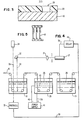
- FIG. 1 shows a flow chart of the process steps which are performed in accordance with this invention.
- Each block in the block diagram represents both a process step and a tank for containing a processing liquid.
- the tank is also used for performing the processing step.
- Tank 11 is the first tank in a series of tanks for continuous processing of materials to be plated or etched.
- Tank 11 receives work which is first introduced as a continuous sheet or as individual workpieces mounted on a carrier material such as a conveyor belt or conveyor chain drive, as with punched work 10 in FIG. 5 formed with integral means for being chain driven.
- the solution in the first tank 11 is adapted to precleaning with an alkaline cleaner in order to remove grease.
- a suitable commercially available product is Alkonox (which is the trade name for a wetting agent and detergent marketed by Alkonox Inc. N.Y., N.Y. 10003) with the workpiece being held in the first tank typically for about two to five minutes at about 65°C.
- step B the work coming out of tank 11 is introduced into tank 12, where it is rinsed. Parts can be sprayed with water for 30 to 60 sec.
- Tank 13 is an etching tank which receives work supplied from tank 12 where Be/Cu parts are to be processed in the system, here they are introduced into a solution of 25% H 2 S0 4 for 30 sec. to 3 minutes at 40°C.
- the work leaving tank 13 passes into tank 14 where it is rinsed in distilled or deionized water for about 30 to 60 sec. as in step B.
- the product from the tank in step 14 is passed into the tank of step 15 where it is etched for 90 sec. in sodium persulfate with a concentration of 20 to 60 grams/liter, which is a typical etchant for Be/Cu parts.
- the work which has been removed from tank 15 is now plated in a nickel plating bath 16 which typically electroplates to a thickness of about 1 to 2 micrometers for use in electronic applications. This requires on the order of about two to ten minutes.
- the output work product from tank 16 is now passed to tank 17 where the parts are rinsed in distilled or deionized water but are not dried in order to prepare them for plating.
- the above steps are employed to prepare the performance of the novel steps described below.
- At this step in the process of sample preparation there are two alternative techniques which can be followed. 1) Laser ablation can be employed to provide selective plating through a mask 28 deposited as described below. 2) Alternatively, laser enhanced plating (which does not involve the use of a mask at all) can be employed.
- tank 18 which contains the liquid (molten) dielectric material to be coated on every surface of the workpiece by immersing the workpiece in the liquid dielectric material.
- Suitable dielectric materials are polymers such as molten wax, glycol phthalate, paraffin, gelatin, inorganic materials, photoresist and the like.
- the parts are exposed to the liquid dielectric medium for a period of time of about ten seconds or less at a temperature in the range of 80 to 95°C.
- the result is a mask 28 of dielectric medium on all surfaces of the work 10 as shown in FIG. 3 which is adapted to be patterned with openings 29 as described in step I.
- tank 18' is employed to plate the work 10 without any masking.
- Tank 18' contains a gold plating solution instead of the liquid dielectric.
- a laser or an array of lasers is focussed to irradiate the portions of the work to be plated with gold or the like as the work passes through tank 18'. The movement of the laser beams will define the plated pattern.
- Plating may be laser enhanced using either the electroplating or the electroless or exchange plating (thermobattery) techniques described in the above patents.
- step H This is the step of laser ablation performed in tank 19 shown in FIGS. 2 and 4 subsequent to step H when the work 10 is coated with the dielectric mask 28 which is impervious to plating and etching solutions 25 or 26.
- the work can be exposed to one or more Q switched lasers 27 (See Industrial Applications of Lasers, p. 48 by J. F. Ready, Academic Press which describes how the Q of a laser cavity can be altered from a low to high Q values by means of Q spoiling and unspoiling apparatus in the laser equipment).
- a Q switched laser 27 is employed because it is capable of storing energy and subsequently releasing all of the energy extremely quickly, i.e.
- the lasers 27 are employed to remove the dielectric coating where desired in order to provide a patterned mask 28 for electrochemical operations which follow.
- the dielectric mask 28 is removed selectively by forming openings 29 shown in FIG. 3 in a desired pattern by rapid local laser heating with laser beam 30, from laser 27.
- the beams 30 from lasers 27 are focussed by lenses 31, reflected by the mirror 32 and applied to regions of the work 10 where plating or etching is to occur.
- the heat of the laser beam 30 removes the dielectric mask 28 in the desired pattern by dissolving it, ablating it, shattering it due to high differential thermal stresses, or melting it and thereby pulling back the liquid film because of the surface tension forces, or the like.
- the removal is very local and is confined to the area of the work 10 which is illuminated by the laser beam 30.
- the laser is adjusted so that in the ablation step, no damage occurs on the workpiece.
- a laser wavelength is chosen to be transparent to the dielectric but absorbing by the workpiece such as 1.06 mm with photoresist on a nickel plate Be/Cu substrate.
- the laser wavelength can be chosen to be absorbed in the working material, for example an eximer laser (UV) with standard photoresist working material.
- this dissolution process or a similar process for forming a dielectric mask can be performed in the electrochemical bath 25 which is to operate upon the workpiece (as shown in FIG. 2) subsequently, without modifying the effectiveness of the electrochemical (plating or etching) bath 25.
- the power of the laser beam 30 employed will be lower than a level at which the work 10 would be damaged, melted or otherwise modified by the heat of the beam 30, where that is likely to affect a change in the ultimate product.
- Typical pulses will be on the order of 20 ns (20 x 10 -9 sec.) or more in duration.
- the uncovered portions of the work 10 are to be plated (or etched) by conventional etching and plating techniques.
- a photoelectric sensor 33 can be employed in the form of a photocell onto which a beam from a low intensity continuous wave (C.W.) laser 34 is incident.
- C.W. continuous wave
- the photoelectric cell 33 Upon passage of the work 10 between the cell 33 and the laser beam 35 (located either on opposite sides of the work 10 or on the same side with reflection) the photoelectric cell 33 generates a voltage signal which activates the controls of the Q switched laser 27 to discharge the stored energy and produce an output beam.
- a synchronized delay system 40 connected between cell 33 and laser 27 by lines 39 can be employed with a potentiometer which adjusts an RC delay circuit so that the laser 27 is discharged just at the point at which the part to be treated is lined up with the Q switched laser 27.
- the amount of the delay required will depend upon the speed with which the work 10 moves through the tank 19, i.e. the reel speed. If the work is to be plated in the next tank 20 as in FIG. 4, then the work 10 is sprayed with water to prevent oxidation of the region of the work which has been exposed during the laser stripping process which has just removed the selected areas 29 in FIG. 3 of the dielectric masking coating 28.
- the lasers are directed to the work 10 by means of the scanning mirror 32 which causes the beam 30 to move. It is possible for the beam 30 to follow the work 10 at the same speed as the work 10 is moving, during a portion of its trip through the tank 19. In general the use of a scanning mirror is not required. If the mirror 32 is stationary, then the laser beam 30 is incident on the work 10 while the work moves relative to the fixed beam 30. To trigger the laser 27, a secondary laser 34 and photocell 33 are used as already described for the ablation technique.
- the speed of the work 10 moving through the plating tank 19 in FIG. 2 and 19 in FIG. 4 is set to result in the appropriate dwell time of the laser 27 and the particular kind of work being treated, to yield the required thickness of the plated film.
- Known (measured) plating rates measured as a function of laser power and dwell time allows one to set the speed of the moving parts at the appropriate level.
- v 0.5 mm/sec.
- the work has a width of 2 mm where the portion of the surface to be plated is located in the center of the 2 mm.
- a delay time of 1.5 sec. is introduced once the part passes the auxiliary trigger laser beam 35 from laser 34 so that plating will start 0.75 mm from the edge of the work area sensed.
- the laser 27 will be turned off after 0.5 sec. by using a circuit (not shown) inside system 27 with a variable time constant set to that value in laser system 27.
- the laser is on for only 0.5 mm per 3 mm of travel. At 0.5 mm of travel/sec., it takes 6 sec. to travel 3 mm, so that the duty cycle is a measure of the number of workpieces per unit time.
- the process can be accelerated by increasing the duty cycle.
- the laser beam 30 defines the pattern to be etched with the workpiece 10 to be etched electrically connected to a power supply 38 as an anode via line 36.
- the laser beam arrays 30 can be activated synchronously.
- Fiber optics can also be employed to direct the beams from the laser to the workpiece, particularly if the solution is highly absorbing or the areas to be plated are not in a direct line of sight readied readily by the laser.
- the current for plating is supplied from cathode line 39 attached electrically from power supply 41 to one of the rollers which contacts the work 10 which is presumed to be conductive.
- the anode is attached to line 40 from the power supply 41.
- FIG. 2 similar connections are shown from the power supply 38 associated with tank 19 which connect the cathode line 36 to a roller in tank 19 which connects to work 10 and the anode line 37.
- the anodes 42 and 43 are suspended in the tanks 19 and 20 respectively in FIGS. 2 and 4.
- a mask dissolving solvent 26 is employed to strip away the remaining portion of the mask 28 from the plated work 10. That is, the mask 28 which was not removed by the laser beam 30 is now removed by the stripping solvent 26 in tank 21.
- suitable stripping solvents 26 for the masking material are listed here. Acetone for photoresist, alcohol for wax or paraffin, acetone for glycol phthalate, or hot water and/or steam under pressure for paraffin or glycol phthalate. The steam may be followed by an additional organic clean up by means of acetone, alcohol and/or freon flurohydrocarbon or other suitable organic residue removal agent or simply by applying heat.
- step L the work 10 moves into a tank 22 which rinses away the residual solvent 26 from the surface of the work 10.
- the tank contains water or uses a water spray (deionized or distilled).
- a method of electrochemically treating a substrate comprising applying a protective film to the substrate, forming a mask on said substrate using an energy beam to remove parts of the film and performing said electrochemical treatment on the substrate through the mask.
Landscapes
- Chemical & Material Sciences (AREA)
- Engineering & Computer Science (AREA)
- Chemical Kinetics & Catalysis (AREA)
- Electrochemistry (AREA)
- Materials Engineering (AREA)
- Metallurgy (AREA)
- Organic Chemistry (AREA)
- Electromagnetism (AREA)
- Physics & Mathematics (AREA)
- Optics & Photonics (AREA)
- Manufacturing & Machinery (AREA)
- Microelectronics & Electronic Packaging (AREA)
- Electroplating Methods And Accessories (AREA)
- Chemically Coating (AREA)
- ing And Chemical Polishing (AREA)
- Laser Beam Processing (AREA)
Applications Claiming Priority (2)
| Application Number | Priority Date | Filing Date | Title |
|---|---|---|---|
| US429657 | 1982-09-30 | ||
| US06/429,657 US4432855A (en) | 1982-09-30 | 1982-09-30 | Automated system for laser mask definition for laser enhanced and conventional plating and etching |
Publications (2)
| Publication Number | Publication Date |
|---|---|
| EP0106977A2 true EP0106977A2 (fr) | 1984-05-02 |
| EP0106977A3 EP0106977A3 (fr) | 1984-08-15 |
Family
ID=23704181
Family Applications (1)
| Application Number | Title | Priority Date | Filing Date |
|---|---|---|---|
| EP83108366A Withdrawn EP0106977A3 (fr) | 1982-09-30 | 1983-08-25 | Procédé et dispositif pour le traitement électrochimique d'un substrat |
Country Status (3)
| Country | Link |
|---|---|
| US (1) | US4432855A (fr) |
| EP (1) | EP0106977A3 (fr) |
| JP (1) | JPS5970755A (fr) |
Cited By (8)
| Publication number | Priority date | Publication date | Assignee | Title |
|---|---|---|---|---|
| EP0337658A1 (fr) * | 1988-04-12 | 1989-10-18 | The Whitaker Corporation | Plaquage sélectif par ablation au laser |
| WO1990012481A1 (fr) * | 1989-04-11 | 1990-10-18 | Northern Telecom Limited | Procede de fabrication d'un outil d'impression |
| WO1993014249A1 (fr) * | 1992-01-10 | 1993-07-22 | Ian Leonard | Procedes et appareils d'usinage electrochimique |
| WO1999045179A1 (fr) * | 1998-03-05 | 1999-09-10 | Obducat Ab | Procede d'attaque |
| DE19934584A1 (de) * | 1999-07-23 | 2001-01-25 | Inovan Stroebe | Verfahren zum Herstellen von Kontakten |
| EP1409772B2 (fr) † | 2001-07-20 | 2008-08-13 | Imo Ingo Müller E.K. | Procede pour la galvanisation selective d'un materiau support metallique en forme de bande |
| KR100903712B1 (ko) * | 2005-12-27 | 2009-06-19 | 닛본 덴끼 가부시끼가이샤 | 부호화 데이터 출력 방법 및 장치, 재부호화 데이터 생성방법 및 장치, 부호화 데이터 복원 방법 및 장치, 부호화방법 및 장치, 및 컴퓨터 판독 가능한 기록 매체 |
| EP4048037A1 (fr) * | 2021-02-19 | 2022-08-24 | Toyota Jidosha Kabushiki Kaisha | Procédé de fabrication de carte de câblage |
Families Citing this family (35)
| Publication number | Priority date | Publication date | Assignee | Title |
|---|---|---|---|---|
| JPS62185892A (ja) * | 1986-02-10 | 1987-08-14 | Kurihara Tokin Kojo:Kk | 電気メツキによる立体的模様形成方法 |
| US4832798A (en) * | 1987-12-16 | 1989-05-23 | Amp Incorporated | Method and apparatus for plating composite |
| GB8825219D0 (en) * | 1988-10-27 | 1988-11-30 | Mbm Technology Ltd | Fine featured electrical circuits |
| JPH0222493A (ja) * | 1989-05-30 | 1990-01-25 | Mitsubishi Electric Corp | 加工装置 |
| US5258098A (en) * | 1991-06-17 | 1993-11-02 | Cycam, Inc. | Method of production of a surface adapted to promote adhesion |
| DE4229399C2 (de) * | 1992-09-03 | 1999-05-27 | Deutsch Zentr Luft & Raumfahrt | Verfahren und Vorrichtung zum Herstellen einer Funktionsstruktur eines Halbleiterbauelements |
| US5641391A (en) * | 1995-05-15 | 1997-06-24 | Hunter; Ian W. | Three dimensional microfabrication by localized electrodeposition and etching |
| JPH1098251A (ja) * | 1996-09-23 | 1998-04-14 | Matsushita Electric Ind Co Ltd | 蒸着された金属配線および誘電配線のuvレーザーアニーリングおよび洗浄 |
| US6211080B1 (en) | 1996-10-30 | 2001-04-03 | Matsushita Electric Industrial Co., Ltd. | Repair of dielectric-coated electrode or circuit defects |
| US6180912B1 (en) | 1998-03-31 | 2001-01-30 | Matsushita Electric Industrial Co., Ltd. | Fan-out beams for repairing an open defect |
| US6060127A (en) * | 1998-03-31 | 2000-05-09 | Matsushita Electric Industrial Co., Ltd. | Mechanically restricted laser deposition |
| SG76591A1 (en) * | 1999-02-27 | 2000-11-21 | Aem Tech Engineers Pte Ltd | Method for selective plating of a metal substrate using laser developed masking layer and apparatus for carrying out the method |
| US20060030149A1 (en) * | 2004-08-06 | 2006-02-09 | Steven Leith | Depositing material on photosensitive material |
| US8496799B2 (en) * | 2005-02-08 | 2013-07-30 | The Trustees Of Columbia University In The City Of New York | Systems and methods for in situ annealing of electro- and electroless platings during deposition |
| US8529738B2 (en) * | 2005-02-08 | 2013-09-10 | The Trustees Of Columbia University In The City Of New York | In situ plating and etching of materials covered with a surface film |
| WO2007027907A2 (fr) * | 2005-09-02 | 2007-03-08 | The Trustees Of Columbia University In The City Of New York | Systeme et procede d'obtention d'une gravure anisotrope de substrats a motifs |
| DE112007001818T5 (de) * | 2006-08-07 | 2009-06-10 | AUTONETWORKS Technologies, LTD., Yokkaichi | Verfahren zum teilweisen Plattieren, Laserplattiervorrichtung und plattiertes Material |
| JP4833762B2 (ja) * | 2006-08-07 | 2011-12-07 | 株式会社オートネットワーク技術研究所 | 部分めっき方法およびコネクタ端子ならびにコネクタ端子の製造方法 |
| US7633035B2 (en) * | 2006-10-05 | 2009-12-15 | Mu-Gahat Holdings Inc. | Reverse side film laser circuit etching |
| US20080083706A1 (en) * | 2006-10-05 | 2008-04-10 | Mu-Gahat Enterprises, Llc | Reverse side film laser circuit etching |
| WO2008070786A1 (fr) * | 2006-12-06 | 2008-06-12 | The Trustees Of Columbia University In The City Of New York | Système microfluidique et procédé pour trier des compositions de bain de placage et d'attaque chimique |
| US20090061251A1 (en) * | 2007-08-27 | 2009-03-05 | Mu-Gahat Enterprises, Llc | Laser circuit etching by additive deposition |
| US20090061112A1 (en) * | 2007-08-27 | 2009-03-05 | Mu-Gahat Enterprises, Llc | Laser circuit etching by subtractive deposition |
| WO2009124180A2 (fr) * | 2008-04-02 | 2009-10-08 | The Trustees Of Columbia University In The City Of New York | Application de dépôt in situ et soudage de matériaux recouverts d’un film superficiel |
| US8985050B2 (en) * | 2009-11-05 | 2015-03-24 | The Trustees Of Columbia University In The City Of New York | Substrate laser oxide removal process followed by electro or immersion plating |
| DE112011100039B4 (de) * | 2010-06-14 | 2014-01-02 | Mitsubishi Electric Corp. | Laserbearbeitungsvorrichtung und Laserbearbeitungsverfahren |
| CN101863394A (zh) * | 2010-06-30 | 2010-10-20 | 佛山塑料集团股份有限公司 | 一种在塑料薄膜上加工图案的工艺 |
| JP5472950B2 (ja) * | 2012-06-19 | 2014-04-16 | Jeインターナショナル株式会社 | マスキング剤および表面処理基材の製造方法 |
| CN102817051B (zh) * | 2012-09-14 | 2015-02-11 | 中国科学院半导体研究所 | 一种激光脉冲电镀系统 |
| CN102925938B (zh) * | 2012-09-14 | 2015-06-03 | 中国科学院半导体研究所 | 一种对激光镀层进行处理的系统 |
| DE102014017886A1 (de) * | 2014-12-04 | 2016-06-09 | Auto-Kabel Management Gmbh | Verfahren zum Herstellen eines elektrischen Anschlussteils |
| WO2016140661A1 (fr) * | 2015-03-04 | 2016-09-09 | TKS Industrial Company | Procédé et appareil pour enlever les résidus des articles revêtus par électrodéposition |
| KR20250037607A (ko) * | 2015-09-09 | 2025-03-17 | 일렉트로 싸이언티픽 인더스트리이즈 인코포레이티드 | 작업물들을 레이저 가공하기 위한 레이저 가공 장치, 방법들 및 관련된 배열들 |
| CN116377533A (zh) * | 2023-04-12 | 2023-07-04 | 汕尾市栢林电子封装材料有限公司 | 一种基于电子基板的局部镀金方法 |
| CN119320968A (zh) * | 2024-11-01 | 2025-01-17 | 深圳市和美科技有限公司 | 局部电镀工艺及电镀系统 |
Family Cites Families (4)
| Publication number | Priority date | Publication date | Assignee | Title |
|---|---|---|---|---|
| US3791938A (en) * | 1971-11-22 | 1974-02-12 | R Healy | Method and apparatus for fabricating selectively plated electrical contacts |
| JPS4946168A (fr) * | 1972-09-11 | 1974-05-02 | ||
| US4217183A (en) * | 1979-05-08 | 1980-08-12 | International Business Machines Corporation | Method for locally enhancing electroplating rates |
| DE3037271A1 (de) * | 1980-10-02 | 1982-05-19 | Harald 5840 Schwerte Albrecht | Verfahren zur glaettung von metallisch beschichteten blechen |
-
1982
- 1982-09-30 US US06/429,657 patent/US4432855A/en not_active Expired - Lifetime
-
1983
- 1983-06-20 JP JP58109441A patent/JPS5970755A/ja active Granted
- 1983-08-25 EP EP83108366A patent/EP0106977A3/fr not_active Withdrawn
Cited By (9)
| Publication number | Priority date | Publication date | Assignee | Title |
|---|---|---|---|---|
| EP0337658A1 (fr) * | 1988-04-12 | 1989-10-18 | The Whitaker Corporation | Plaquage sélectif par ablation au laser |
| WO1990012481A1 (fr) * | 1989-04-11 | 1990-10-18 | Northern Telecom Limited | Procede de fabrication d'un outil d'impression |
| WO1993014249A1 (fr) * | 1992-01-10 | 1993-07-22 | Ian Leonard | Procedes et appareils d'usinage electrochimique |
| WO1999045179A1 (fr) * | 1998-03-05 | 1999-09-10 | Obducat Ab | Procede d'attaque |
| US6423207B1 (en) | 1998-03-05 | 2002-07-23 | Obducat Ab | Method and apparatus for etching |
| DE19934584A1 (de) * | 1999-07-23 | 2001-01-25 | Inovan Stroebe | Verfahren zum Herstellen von Kontakten |
| EP1409772B2 (fr) † | 2001-07-20 | 2008-08-13 | Imo Ingo Müller E.K. | Procede pour la galvanisation selective d'un materiau support metallique en forme de bande |
| KR100903712B1 (ko) * | 2005-12-27 | 2009-06-19 | 닛본 덴끼 가부시끼가이샤 | 부호화 데이터 출력 방법 및 장치, 재부호화 데이터 생성방법 및 장치, 부호화 데이터 복원 방법 및 장치, 부호화방법 및 장치, 및 컴퓨터 판독 가능한 기록 매체 |
| EP4048037A1 (fr) * | 2021-02-19 | 2022-08-24 | Toyota Jidosha Kabushiki Kaisha | Procédé de fabrication de carte de câblage |
Also Published As
| Publication number | Publication date |
|---|---|
| JPS5970755A (ja) | 1984-04-21 |
| US4432855A (en) | 1984-02-21 |
| JPH0253511B2 (fr) | 1990-11-16 |
| EP0106977A3 (fr) | 1984-08-15 |
Similar Documents
| Publication | Publication Date | Title |
|---|---|---|
| US4432855A (en) | Automated system for laser mask definition for laser enhanced and conventional plating and etching | |
| JP2524458B2 (ja) | 電気化学マイクロマシニング方法 | |
| US4349583A (en) | Laser enhanced maskless method for plating and simultaneous plating and etching of patterns | |
| US5011567A (en) | Method of fabricating solar cells | |
| EP0019064B1 (fr) | Procédé d'enlèvement sélectif de matériau par voie chimique ou électrochimique | |
| US4359485A (en) | Radiation induced deposition of metal on semiconductor surfaces | |
| EP0180101B1 (fr) | Dépôt d'une configuration en utilisant l'ablation par laser | |
| EP1155168B1 (fr) | Procede de placage selectif de substrat metallique utilisant une couche de masquage obtenue par laser et appareil a cet effet | |
| EP0357124B1 (fr) | Procédé pour appliquer sélectivement un métal à partir de la phase liquide sur un substrat à l'aide d'un laser | |
| Nowak et al. | Thermochemical laser etching of stainless steel and titanium in liquids | |
| US20110042201A1 (en) | In situ Plating And Soldering Of Materials Covered With A Surface Film | |
| US8985050B2 (en) | Substrate laser oxide removal process followed by electro or immersion plating | |
| US5961860A (en) | Pulse laser induced removal of mold flash on integrated circuit packages | |
| US4426442A (en) | Method of producing metal images or patterns on and/or below the surface of a substrate comprising a semiconducting light-sensitive compound | |
| US5192581A (en) | Protective layer for preventing electroless deposition on a dielectric | |
| DE3751551T2 (de) | Lithographisches Verfahren unter Anwendung von Laser zur Herstellung von elektronischen Elementen und ähnlichen. | |
| US20020102745A1 (en) | Process for modifying chip assembly substrates | |
| US20020096433A1 (en) | Method for electrodeposited film formation, method for electrode formation, and apparatus for electrodeposited film formation | |
| Metev et al. | Pattern generation by laser-induced oxidation of thin metal films (microcircuit fabrication) | |
| WO2012156034A1 (fr) | Procédé et appareil pour la fabrication de grilles de connexion | |
| US3663388A (en) | Gold removal process | |
| JPS60149783A (ja) | 選択的メツキ方法 | |
| JP2553926B2 (ja) | 選択的金属薄膜の形成方法 | |
| Von Gutfeld | Laser enhanced plating and etching: A review | |
| Williams et al. | The patterning of fine-pitch electrical interconnections on non-planar substrates: a comparison between methods utilising laser ablation and electro-deposited photoresist |
Legal Events
| Date | Code | Title | Description |
|---|---|---|---|
| PUAI | Public reference made under article 153(3) epc to a published international application that has entered the european phase |
Free format text: ORIGINAL CODE: 0009012 |
|
| AK | Designated contracting states |
Designated state(s): DE FR GB |
|
| PUAL | Search report despatched |
Free format text: ORIGINAL CODE: 0009013 |
|
| AK | Designated contracting states |
Designated state(s): DE FR GB |
|
| 17P | Request for examination filed |
Effective date: 19840724 |
|
| STAA | Information on the status of an ep patent application or granted ep patent |
Free format text: STATUS: THE APPLICATION IS DEEMED TO BE WITHDRAWN |
|
| 18D | Application deemed to be withdrawn |
Effective date: 19860216 |
|
| RIN1 | Information on inventor provided before grant (corrected) |
Inventor name: VON GUTFELD, ROBERT JACOB Inventor name: ROMANKIW, LUBOMYR TARAS |