EP0107387A2 - Halbleiterspeicheranordnung - Google Patents
Halbleiterspeicheranordnung Download PDFInfo
- Publication number
- EP0107387A2 EP0107387A2 EP83305837A EP83305837A EP0107387A2 EP 0107387 A2 EP0107387 A2 EP 0107387A2 EP 83305837 A EP83305837 A EP 83305837A EP 83305837 A EP83305837 A EP 83305837A EP 0107387 A2 EP0107387 A2 EP 0107387A2
- Authority
- EP
- European Patent Office
- Prior art keywords
- column lines
- lines
- column
- sense amplifiers
- storage cells
- Prior art date
- Legal status (The legal status is an assumption and is not a legal conclusion. Google has not performed a legal analysis and makes no representation as to the accuracy of the status listed.)
- Withdrawn
Links
Images


Classifications
-
- G—PHYSICS
- G11—INFORMATION STORAGE
- G11C—STATIC STORES
- G11C11/00—Digital stores characterised by the use of particular electric or magnetic storage elements; Storage elements therefor
- G11C11/21—Digital stores characterised by the use of particular electric or magnetic storage elements; Storage elements therefor using electric elements
- G11C11/34—Digital stores characterised by the use of particular electric or magnetic storage elements; Storage elements therefor using electric elements using semiconductor devices
- G11C11/40—Digital stores characterised by the use of particular electric or magnetic storage elements; Storage elements therefor using electric elements using semiconductor devices using transistors
- G11C11/401—Digital stores characterised by the use of particular electric or magnetic storage elements; Storage elements therefor using electric elements using semiconductor devices using transistors forming cells needing refreshing or charge regeneration, i.e. dynamic cells
- G11C11/4063—Auxiliary circuits, e.g. for addressing, decoding, driving, writing, sensing or timing
- G11C11/407—Auxiliary circuits, e.g. for addressing, decoding, driving, writing, sensing or timing for memory cells of the field-effect type
- G11C11/409—Read-write [R-W] circuits
- G11C11/4096—Input/output [I/O] data management or control circuits, e.g. reading or writing circuits, I/O drivers or bit-line switches
-
- G—PHYSICS
- G11—INFORMATION STORAGE
- G11C—STATIC STORES
- G11C11/00—Digital stores characterised by the use of particular electric or magnetic storage elements; Storage elements therefor
- G11C11/21—Digital stores characterised by the use of particular electric or magnetic storage elements; Storage elements therefor using electric elements
- G11C11/34—Digital stores characterised by the use of particular electric or magnetic storage elements; Storage elements therefor using electric elements using semiconductor devices
- G11C11/40—Digital stores characterised by the use of particular electric or magnetic storage elements; Storage elements therefor using electric elements using semiconductor devices using transistors
- G11C11/401—Digital stores characterised by the use of particular electric or magnetic storage elements; Storage elements therefor using electric elements using semiconductor devices using transistors forming cells needing refreshing or charge regeneration, i.e. dynamic cells
- G11C11/406—Management or control of the refreshing or charge-regeneration cycles
-
- G—PHYSICS
- G11—INFORMATION STORAGE
- G11C—STATIC STORES
- G11C11/00—Digital stores characterised by the use of particular electric or magnetic storage elements; Storage elements therefor
- G11C11/21—Digital stores characterised by the use of particular electric or magnetic storage elements; Storage elements therefor using electric elements
- G11C11/34—Digital stores characterised by the use of particular electric or magnetic storage elements; Storage elements therefor using electric elements using semiconductor devices
- G11C11/40—Digital stores characterised by the use of particular electric or magnetic storage elements; Storage elements therefor using electric elements using semiconductor devices using transistors
- G11C11/401—Digital stores characterised by the use of particular electric or magnetic storage elements; Storage elements therefor using electric elements using semiconductor devices using transistors forming cells needing refreshing or charge regeneration, i.e. dynamic cells
- G11C11/4063—Auxiliary circuits, e.g. for addressing, decoding, driving, writing, sensing or timing
- G11C11/407—Auxiliary circuits, e.g. for addressing, decoding, driving, writing, sensing or timing for memory cells of the field-effect type
- G11C11/408—Address circuits
- G11C11/4087—Address decoders, e.g. bit - or word line decoders; Multiple line decoders
Definitions
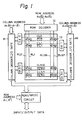
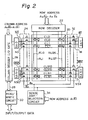
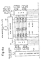
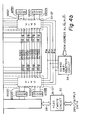
- the present invention only the sense amplifiers disposed on one side of the storage cells array are used for read out or write in operations of the storage cells.
- two column decoders are not necessary. Only a single column decoder need be provided for the storage cell array, even though sense amplifiers are disposed on both sides of the array. Therefore, the pitch of storage cells can be narrowed without increasing the pattern area of the memory device and also without decreasing the access speed which would occur with a heavy load of the address lines.
Landscapes
- Engineering & Computer Science (AREA)
- Microelectronics & Electronic Packaging (AREA)
- Computer Hardware Design (AREA)
- Databases & Information Systems (AREA)
- Dram (AREA)
Applications Claiming Priority (2)
| Application Number | Priority Date | Filing Date | Title |
|---|---|---|---|
| JP167522/82 | 1982-09-28 | ||
| JP57167522A JPS5958689A (ja) | 1982-09-28 | 1982-09-28 | 半導体記憶装置 |
Publications (2)
| Publication Number | Publication Date |
|---|---|
| EP0107387A2 true EP0107387A2 (de) | 1984-05-02 |
| EP0107387A3 EP0107387A3 (de) | 1986-10-15 |
Family
ID=15851251
Family Applications (1)
| Application Number | Title | Priority Date | Filing Date |
|---|---|---|---|
| EP83305837A Withdrawn EP0107387A3 (de) | 1982-09-28 | 1983-09-28 | Halbleiterspeicheranordnung |
Country Status (3)
| Country | Link |
|---|---|
| US (1) | US4581720A (de) |
| EP (1) | EP0107387A3 (de) |
| JP (1) | JPS5958689A (de) |
Families Citing this family (23)
| Publication number | Priority date | Publication date | Assignee | Title |
|---|---|---|---|---|
| US4630240A (en) * | 1984-07-02 | 1986-12-16 | Texas Instruments Incorporated | Dynamic memory with intermediate column derode |
| JPS6134792A (ja) * | 1984-07-25 | 1986-02-19 | Toshiba Corp | 半導体記憶装置 |
| US4800525A (en) * | 1984-10-31 | 1989-01-24 | Texas Instruments Incorporated | Dual ended folded bit line arrangement and addressing scheme |
| JPS61242396A (ja) * | 1985-04-19 | 1986-10-28 | Nec Corp | 半導体メモリ |
| US5197033A (en) * | 1986-07-18 | 1993-03-23 | Hitachi, Ltd. | Semiconductor device incorporating internal power supply for compensating for deviation in operating condition and fabrication process conditions |
| US4710902A (en) * | 1985-10-04 | 1987-12-01 | Motorola, Inc. | Technique restore for a dynamic random access memory |
| US4807194A (en) * | 1986-04-24 | 1989-02-21 | Matsushita Electric Industrial Co., Ltd. | Seimiconductor memory device having sub bit lines |
| JPS63104296A (ja) * | 1986-10-21 | 1988-05-09 | Nec Corp | 半導体記憶装置 |
| JPS63205897A (ja) * | 1987-02-20 | 1988-08-25 | Matsushita Electric Ind Co Ltd | 半導体記憶装置 |
| US5222047A (en) * | 1987-05-15 | 1993-06-22 | Mitsubishi Denki Kabushiki Kaisha | Method and apparatus for driving word line in block access memory |
| JPH0166698U (de) * | 1987-10-20 | 1989-04-28 | ||
| US5280448A (en) * | 1987-11-18 | 1994-01-18 | Sony Corporation | Dynamic memory with group bit lines and associated bit line group selector |
| JPH01158694A (ja) * | 1987-12-15 | 1989-06-21 | Mitsubishi Electric Corp | 半導体ダイナミックram |
| EP0321847B1 (de) * | 1987-12-21 | 1994-06-29 | Kabushiki Kaisha Toshiba | Halbleiterspeicher, der fähig zur Verbesserung der Datenwiedereinschreibgeschwindigkeit ist |
| JP2691280B2 (ja) * | 1988-05-12 | 1997-12-17 | 三菱電機株式会社 | 半導体記憶装置 |
| JPH0271493A (ja) * | 1988-09-06 | 1990-03-12 | Mitsubishi Electric Corp | 半導体メモリ装置 |
| JP2633645B2 (ja) * | 1988-09-13 | 1997-07-23 | 株式会社東芝 | 半導体メモリ装置 |
| US5034920A (en) * | 1988-10-12 | 1991-07-23 | Texas Instruments Incorporated | Cross point array memory device |
| JP2723683B2 (ja) * | 1991-02-25 | 1998-03-09 | 日本電気アイシーマイコンシステム株式会社 | 半導体記憶装置 |
| US5465339A (en) * | 1991-02-27 | 1995-11-07 | Vlsi Technology, Inc. | Decoupled refresh on local and system busses in a PC/at or similar microprocessor environment |
| US5291443A (en) * | 1991-06-26 | 1994-03-01 | Micron Technology, Inc. | Simultaneous read and refresh of different rows in a dram |
| US5636158A (en) * | 1995-03-13 | 1997-06-03 | Kabushiki Kaisha Toshiba | Irregular pitch layout for a semiconductor memory device |
| JPH10241354A (ja) * | 1997-02-21 | 1998-09-11 | Mitsubishi Electric Corp | 双方向転送型記憶装置及びメモリの入出力制御方法 |
Family Cites Families (4)
| Publication number | Priority date | Publication date | Assignee | Title |
|---|---|---|---|---|
| US3599180A (en) * | 1968-11-29 | 1971-08-10 | Gen Instrument Corp | Random access read-write memory system having data refreshing capabilities and memory cell therefor |
| JPS6048074B2 (ja) * | 1978-02-09 | 1985-10-25 | 日本電気株式会社 | メモリ回路 |
| US4203159A (en) * | 1978-10-05 | 1980-05-13 | Wanlass Frank M | Pseudostatic electronic memory |
| JPS5942399B2 (ja) * | 1979-12-21 | 1984-10-15 | 株式会社日立製作所 | メモリ装置 |
-
1982
- 1982-09-28 JP JP57167522A patent/JPS5958689A/ja active Pending
-
1983
- 1983-09-26 US US06/535,836 patent/US4581720A/en not_active Expired - Fee Related
- 1983-09-28 EP EP83305837A patent/EP0107387A3/de not_active Withdrawn
Also Published As
| Publication number | Publication date |
|---|---|
| EP0107387A3 (de) | 1986-10-15 |
| US4581720A (en) | 1986-04-08 |
| JPS5958689A (ja) | 1984-04-04 |
Similar Documents
| Publication | Publication Date | Title |
|---|---|---|
| EP0107387A2 (de) | Halbleiterspeicheranordnung | |
| US5111434A (en) | Semiconductor memory device | |
| EP0068645B1 (de) | Halbleiterspeicheranlage | |
| US5970006A (en) | Semiconductor memory device having cell array divided into a plurality of cell blocks | |
| US4367540A (en) | Dynamic memory with an interchangeable pair of data lines and sense amplifiers | |
| KR950010758B1 (ko) | 다이나믹형 메모리 | |
| US4920517A (en) | Semiconductor memory device having sub bit lines | |
| US5148401A (en) | DRAM with split word lines | |
| US4418399A (en) | Semiconductor memory system | |
| KR910000388B1 (ko) | 메모리셀 블록의 선택적 동작이 가능한 반도체 메모리장치 | |
| EP0107340B1 (de) | Halbleiterspeicher des Zwei-Gattern-Typs | |
| KR100300622B1 (ko) | 반도체 기억장치 | |
| US4680734A (en) | Semiconductor memory device | |
| KR100824798B1 (ko) | 에지 서브 어레이에 전체 데이터 패턴을 기입할 수 있는 오픈 비트 라인 구조를 가지는 메모리 코어, 이를 구비한 반도체 메모리 장치, 및 에지 서브 어레이 테스트 방법 | |
| US5862072A (en) | Memory array architecture and method for dynamic cell plate sensing | |
| US6330202B1 (en) | Semiconductor memory device having write data line | |
| KR940006996B1 (ko) | 반도체 기억장치 | |
| EP0166642A2 (de) | Blockunterteiltes Halbleiterspeichergerät mit unterteilten Bitzeilen | |
| KR100298973B1 (ko) | 반도체기억장치 | |
| JPH02247890A (ja) | 半導体記憶装置 | |
| US4511997A (en) | Semiconductor memory device | |
| KR950002042A (ko) | 서로 분리된 제 1 및 제 2 입출력선 그룹을 가지는 다이나믹랜덤 엑세스 메모리장치 | |
| KR100267132B1 (ko) | 반도체 기억장치 | |
| US6058067A (en) | Multi-bank semiconductor memory device having an output control circuit for controlling bit line pairs of each bank connected to data bus pairs | |
| US4389714A (en) | Memory device |
Legal Events
| Date | Code | Title | Description |
|---|---|---|---|
| PUAI | Public reference made under article 153(3) epc to a published international application that has entered the european phase |
Free format text: ORIGINAL CODE: 0009012 |
|
| AK | Designated contracting states |
Designated state(s): DE FR GB |
|
| PUAL | Search report despatched |
Free format text: ORIGINAL CODE: 0009013 |
|
| AK | Designated contracting states |
Kind code of ref document: A3 Designated state(s): DE FR GB |
|
| 17P | Request for examination filed |
Effective date: 19870327 |
|
| 17Q | First examination report despatched |
Effective date: 19880115 |
|
| STAA | Information on the status of an ep patent application or granted ep patent |
Free format text: STATUS: THE APPLICATION HAS BEEN WITHDRAWN |
|
| 18W | Application withdrawn |
Withdrawal date: 19900329 |
|
| R18W | Application withdrawn (corrected) |
Effective date: 19900329 |
|
| RIN1 | Information on inventor provided before grant (corrected) |
Inventor name: SATO, KIMIAKI Inventor name: TAKEMAE, YOSHIHIRO Inventor name: NAKANO, TOMIO |