EP0107443A2 - Dünnfilmmagnetkopf für Aufzeichnung oder Wiedergabe - Google Patents
Dünnfilmmagnetkopf für Aufzeichnung oder Wiedergabe Download PDFInfo
- Publication number
- EP0107443A2 EP0107443A2 EP83306171A EP83306171A EP0107443A2 EP 0107443 A2 EP0107443 A2 EP 0107443A2 EP 83306171 A EP83306171 A EP 83306171A EP 83306171 A EP83306171 A EP 83306171A EP 0107443 A2 EP0107443 A2 EP 0107443A2
- Authority
- EP
- European Patent Office
- Prior art keywords
- layer
- magnetic
- magnetic layer
- head
- magnetic pole
- Prior art date
- Legal status (The legal status is an assumption and is not a legal conclusion. Google has not performed a legal analysis and makes no representation as to the accuracy of the status listed.)
- Granted
Links
- 239000010409 thin film Substances 0.000 title claims abstract description 25
- 239000000758 substrate Substances 0.000 claims abstract description 31
- 239000012212 insulator Substances 0.000 claims abstract description 26
- 239000000956 alloy Substances 0.000 claims description 31
- 229910045601 alloy Inorganic materials 0.000 claims description 30
- 239000004020 conductor Substances 0.000 claims description 8
- 229920001721 polyimide Polymers 0.000 claims description 7
- 229910052742 iron Inorganic materials 0.000 claims description 5
- 239000011347 resin Substances 0.000 claims description 4
- 229920005989 resin Polymers 0.000 claims description 4
- 239000004642 Polyimide Substances 0.000 claims description 3
- 239000004615 ingredient Substances 0.000 claims description 3
- 229910001004 magnetic alloy Inorganic materials 0.000 claims description 3
- 238000009413 insulation Methods 0.000 claims 6
- 239000000463 material Substances 0.000 description 15
- 238000000034 method Methods 0.000 description 15
- 230000008569 process Effects 0.000 description 12
- 238000004544 sputter deposition Methods 0.000 description 11
- 239000010408 film Substances 0.000 description 8
- 230000004907 flux Effects 0.000 description 7
- 229910003271 Ni-Fe Inorganic materials 0.000 description 6
- VYPSYNLAJGMNEJ-UHFFFAOYSA-N silicon dioxide Inorganic materials O=[Si]=O VYPSYNLAJGMNEJ-UHFFFAOYSA-N 0.000 description 6
- 229910017082 Fe-Si Inorganic materials 0.000 description 5
- 229910017133 Fe—Si Inorganic materials 0.000 description 5
- 238000004519 manufacturing process Methods 0.000 description 5
- 230000035699 permeability Effects 0.000 description 5
- 229910052681 coesite Inorganic materials 0.000 description 4
- 238000010276 construction Methods 0.000 description 4
- 229910052906 cristobalite Inorganic materials 0.000 description 4
- 230000000694 effects Effects 0.000 description 4
- 238000010292 electrical insulation Methods 0.000 description 4
- 238000005530 etching Methods 0.000 description 4
- 238000000059 patterning Methods 0.000 description 4
- 239000009719 polyimide resin Substances 0.000 description 4
- 229910052682 stishovite Inorganic materials 0.000 description 4
- 229910052905 tridymite Inorganic materials 0.000 description 4
- 229910019580 Cr Zr Inorganic materials 0.000 description 3
- 229910019817 Cr—Zr Inorganic materials 0.000 description 3
- 229910000808 amorphous metal alloy Inorganic materials 0.000 description 3
- 230000015556 catabolic process Effects 0.000 description 3
- 238000006731 degradation reaction Methods 0.000 description 3
- 230000008020 evaporation Effects 0.000 description 3
- 238000001704 evaporation Methods 0.000 description 3
- SDQJTWBNWQABLE-UHFFFAOYSA-N 1h-quinazoline-2,4-dione Chemical compound C1=CC=C2C(=O)NC(=O)NC2=C1 SDQJTWBNWQABLE-UHFFFAOYSA-N 0.000 description 2
- 230000015572 biosynthetic process Effects 0.000 description 2
- 229910052804 chromium Inorganic materials 0.000 description 2
- 239000011521 glass Substances 0.000 description 2
- 238000003754 machining Methods 0.000 description 2
- 239000000203 mixture Substances 0.000 description 2
- 238000007747 plating Methods 0.000 description 2
- 239000000377 silicon dioxide Substances 0.000 description 2
- 239000000126 substance Substances 0.000 description 2
- 229910000859 α-Fe Inorganic materials 0.000 description 2
- 229910020517 Co—Ti Inorganic materials 0.000 description 1
- 229910000599 Cr alloy Inorganic materials 0.000 description 1
- 208000004221 Multiple Trauma Diseases 0.000 description 1
- 229910020018 Nb Zr Inorganic materials 0.000 description 1
- 229910000929 Ru alloy Inorganic materials 0.000 description 1
- 229910001069 Ti alloy Inorganic materials 0.000 description 1
- XAGFODPZIPBFFR-UHFFFAOYSA-N aluminium Chemical compound [Al] XAGFODPZIPBFFR-UHFFFAOYSA-N 0.000 description 1
- 229910052782 aluminium Inorganic materials 0.000 description 1
- 239000004411 aluminium Substances 0.000 description 1
- 239000000919 ceramic Substances 0.000 description 1
- 238000005520 cutting process Methods 0.000 description 1
- 230000007547 defect Effects 0.000 description 1
- 230000002349 favourable effect Effects 0.000 description 1
- 230000004048 modification Effects 0.000 description 1
- 238000012986 modification Methods 0.000 description 1
- 229910052759 nickel Inorganic materials 0.000 description 1
- 229910000889 permalloy Inorganic materials 0.000 description 1
- 238000001259 photo etching Methods 0.000 description 1
- 230000009467 reduction Effects 0.000 description 1
- 229910052726 zirconium Inorganic materials 0.000 description 1
Images

Classifications
-
- G—PHYSICS
- G11—INFORMATION STORAGE
- G11B—INFORMATION STORAGE BASED ON RELATIVE MOVEMENT BETWEEN RECORD CARRIER AND TRANSDUCER
- G11B5/00—Recording by magnetisation or demagnetisation of a record carrier; Reproducing by magnetic means; Record carriers therefor
- G11B5/127—Structure or manufacture of heads, e.g. inductive
- G11B5/1278—Structure or manufacture of heads, e.g. inductive specially adapted for magnetisations perpendicular to the surface of the record carrier
Definitions
- the present invention relates to a magnetic recording and reproducing thin film head.
- Figure 1 of the accompanying drawings shows one example of such a head.
- a lower magnetic layer 2 is formed on a nonmagnetic substrate 1.
- An inorganic insulator layer 3 effects electrical insulation between the lower magnetic layer 2 and a conductor coil 4
- an organic insulator 5 layer effects electrical insulation between the conductor coil 4 and an upper magnetic layer 6 formed of a magnetic film of high permeability. It is required that one magnetic layer of a magnetic recording head be very thin to form a main magnetic pole for executing recording and reproduction, while the other magnetic layer very thick to form an auxiliary magnetic pole for forming a closed magnetic path (see, for example, Japanese Laid-open Patent Application No. 52-82318).
- the lower magnetic layer is thickened and forms the auxiliary magnetic pole. It is also known to form the substrate of a magnetic substrate such as Mn-Zn ferrite so that the substrate functions both as the lower magnetic layer and as a substrate (see, for example, Japanese Laid-open Utility Model Registration Application No. 57-75617).
- the upper magnetic layer forms a high step pattern (ordinarily, a step of approximately 10 ⁇ m), so the magnetic characteristics are liable to degrade at the step part, and that due to the multi-turning of the coil intended to enhance the current efficiency, an undulation (small unevenness) corresponding to the coil pattern may appear in the upper magnetic layer, so the magnetic characteristics degrade.
- Another disadvantage is that high dimensional accuracy of the main magnetic pole is not achieved either when the high step is patterned by etching or when the pattern is formed by a process such as sputtering with a mask. Particularly when the upper magnetic layer is thick, accurate patterning is impossible to achieve or practice. It is therefore difficult to thicken any part other than part A (shown in Figure 1) concerned in the recording and reproduction and which faces a magnetic recording medium, which would have the effect of reducing the magnetic reluctance and raising the efficiency of the head.
- the present invention seeks to overcome the problem of degradation of magnetic characteristics inherent in the prior art thin film head.
- the inventors of the present invention have appreciated that since the main magnetic pole determining the head performance is the upper magnetic layer in the prior art, it is the defect of the layer which are primarily responsible for the degradation of magnetic characteristics of the head. Therefore the present invention proposes that the main magnetic pole is formed by the lower magnetic layer, the upper layer forming the auxiliary magnetic pole.
- the lower magnetic layer is formed on the (flat and non-magnetic) substrate and hence it is easier to produce an even layer and to pattern the layer.
- the present invention thus makes possible a thin film head which has a high recording density, high recording and reproduction efficiency, and excellent magnetic characteristics, and which is relatively easy to manufacture.
- the thicknesses of the lower magnetic layer and the upper magnetic layer respectively may be similar to those of the main magnetic pole and the auxiliary magnetic pole of the prior art constructions.
- that part of the main magnetic pole which in use faces the magnetic recording medium is 2 to 5 ⁇ m long and 0.1 to 1 ⁇ m thick, the other part of the main magnetic pole being 1 to 6 ⁇ m thick, and the auxiliary magnetic pole is 5 to 60 um thick.
- the main magnetic pole may have a uniform thickness of, for example, 0.1 ⁇ m to 1 ⁇ m.
- the lower magnetic layer formed on the nonmagnetic substrate serves as the main magnetic pole. Therefore, in order to prevent a gap (which would degrade the characteristics of the device) from arising between the magnetic recording medium and the main magnetic pole during operation, the angle 9 which the surface of the substrate facing the recording medium defines to the upper surface of the substrate, which has the lower magnetic layer thereon, should preferably be 60° to 87°, more preferably 80° to 85°, not 90°. However, even when the angle is 90°, as in the prior art, the effects of the present invention may be obtained.
- the upper magnetic layer of a thin film head according to the present invention can be formed by a process such as sputtering with a mask, evaporation with a mask or plating, and it need not undergo etching on step.
- the pattern of the upper magnetic layer may be formed via photoetching a step, as in the prior art, if desired.
- the upper magnetic layer is the auxiliary magnetic pole, it is thick, and formation by etching is often difficult.
- the material for the upper magnetic layer and the lower magnetic layer may be those used in prior art heads.
- materials of high permeability which can be formed into thin films for example, permalloys (Ni-Fe alloys) and amorphous magnetic alloys of high permeability (Co-Cr-Zr alloys etc.) are used.
- a material of high saturation flux density is desirable for the upper magnetic layer serving as the main magnetic pole.
- a vertical section through the principal portions of an embodiment of a magnetic perpendicular magnetic recording and reproducing thin film head according to the present invention shows, a nonmagnetic substrate 10 made, for example, of "Photoceram” (trade name of Corning Glass Works) which was 40 mm in diameter and 1 mm in thickness. It is also possible to use a nonmagnetic substrate made of "7059 Glass” (trade name of Corning Glass Works) of ceramics such as A1 2 0 3 or A1 2 0 3 -Tic.
- a lower magnetic layer 11 is formed by a sputtering process with a target having a composition of 77.5 wt% Ni - 22.5 wt% Fe on the substrate.
- the thickness of the lower magnetic layer 11 in the vicinity of a part B facing to a magnetic recording medium was 0.5 ⁇ m, and the thickness thereof on a rear core side was 3 ⁇ m. It is normally desirable for the thickness of the lower magnetic layer in the vicinity of the face to be approximately 0.1 to 1 ⁇ m and the thickness of the rear core to be approximately 1 to 6 ⁇ m. It is also possible to simplify the manufacturing process by making the rear core and the face to be approximately equal in thickness, although this causes some reduction in efficiency.
- the length D of the thin part of the lower magnetic layer in the vicinity of the face is preferably approximately 2 to 5 ⁇ m, and in the embodiment it was made 2 ⁇ m thick.
- An insulator layer 12 serves for electrical insulation between the lower magnetic layer 11 and the conductor coil 13.
- Si0 2 was deposited to a thickness of 3 ⁇ m by a sputtering process.
- Aluminium (Al) was deposited by evaporation process to form the conductor coil 13.
- the coil 13 was a spiral type multiple-wound coil of four turns whose conductor section was 4 ⁇ m wide and 6 ⁇ m high.
- An organic insulator layer 14 of a polyimide resin or the like was used for electrical insulation between the conductor coil 13 and an upper magnetic layer 15. The organic insulator layer 14 is also flattened the upper surface of the 4-turn multiple coil.
- PIQ (trade name of Hitachi Kasei Kabushiki Kaisha) which is a polyimide isoindro q uinazolinedione resin, was used to form the layer 14.
- the thickness of the PIQ layer 14 as measured from the upper surface of the insulator layer 12 was 6 ⁇ m.
- the step of flattening the surface above the coil by utilizing the viscosity of PIQ is already known.
- the insulator layer needs to be as flat as possible in order to prevent degradation of the magnetic characteristics of the upper magnetic layer, being the main magnetic pole.
- the insulator layer 14 need not be very flat because a thick auxiliary magnetic pole is formed thereon.
- the insulator may, therefore, be made of an inorganic insulator such as Si0 2 rather than an organic substrate.
- patterning was carried out by the use of a photo- lithograph technique.
- Such techniques and the structure of parts of the head according to the present invention other than the principal portions are the same as in the prior art, and further description is not given here.
- An amor- p hous alloy composed of 76 at% Co - 12 at% Cr - 12 at% Zr was formed to a thickness of about 20 ⁇ m by a sputtering process to form an upper magnetic layer 15.
- the magnetic layer 15 In order to form the magnetic layer 15 in a desired shape, a mask was placed over the head during the sputtering so as to deposit the magnetic substance on only the desired parts of the head. This is a technique which is usually known as a mask sputtering process.
- a mask sputtering process In general, with mask sputtering a magnetic substance turns round through the clearance between a mask and a specimen and is deposited on the specimen, and registration of a pattern with another pattern formed is difficult, so precision is not high.
- the upper magnetic layer serves as the auxiliary magnetic pole, which pole merely forms a closed magnetic path, and hence, its purpose can be achieved satisfactorily. Since etching etc. for forming a pattern are not performed, the upper magnetic layer 15 may be a thick film. If the magnetic head is to have suitable characteristics it is desirable for the thickness of the upper magnetic layer to be 5 to 40 ⁇ m.
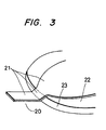
- Figure 3 shows a perspective view of a prior art thin film head.
- the figure shows a lower magnetic layer 15, an upper magnetic layer 21 which serves as the main magnetic pole, an organic insulator layer 22 which covers a coil pattern, and a step part 23 which is formed by part of the organic insulator layer.
- illustration of the shape of the lower magnetic layer 20 is omitted.
- the prior art thin film head involves the disadvantage that, since the upper magnetic layer is used as the main magnetic pole for recording and reproduction, patterning which includes the high step part 23 as shown in Figure 3 is needed, so the dimensional accuracy is inferior.
- the main magnetic pole is the lower magnetic layer and is patterned on the flat substrate, so that the dimensional accuracy is enhanced to improve the available percentage in mass production.
- the head of the present invention may be finished by machining steps such as cutting, lathing and lapping after the proper patterns of the respective layers have been formed on the substrate. Since such steps are known processes, further description is not given here.
- the section of the principal portions shown in Figure 2 corresponds to the final head which has undergone machining steps.
- the surface of the substrate facing the recording medium preferably does not form a right-angle with the surface of the substrate formed with the patterns thereon. The reason for this is to improve the contact between the recording medium and the main magnetic pole and to bring them as close as possible.
- the surface of the substrate facing the recording medium should desirably be in a shape retreating from the plane of the recording medium.
- the angle e was 84°. Such angling can be readily achieved by lapping the surface obliquely.
- the recording and reproducing characteristics of the head of the embodiment of the present invention were measured by the use of a magnetic recording medium in which a perpendicular magnetic film of a Co-Cr alloy layer was formed on an Ni-Fe alloy layer.
- the optimized recording current was approximately 30 mA at a recording density of 10 KBPI, and this was about 1/3 of the value of the prior-art head shown in Figure 1.
- the reproduction output at 1 KBPI was approximately 0.24 mV p-p, which was about 1.5 times that of the prior-art head.
- the prior-art head of Figure 1 used for the comparisons was substantially the same in construction as the head of the present embodiment, except that the lower magnetic layer 2 which was made of Mn-Zn ferrite and which was 1,000 ⁇ m thick was used as the auxiliary magnetic pole and that the upper magnetic layer 6 (0.5 ⁇ m thick) whose side facing to the recording medium was not thinned was used as the main magnetic pole.
- Ni-Fe alloy was used as the material of the main magnetic pole.
- the saturation flux density of this material is about 10 kG. It is preferable to select a material having the highest possible saturation flux density in order to prevent magnetic saturation developing in the main magnetic pole for executing the recording, particularly in the part near to the recording medium.
- an Fe - 6.5 wt% Si - 1 wt% Ru alloy having a saturation flux density of about 18 kG was formed by the sputtering process and used as the material of the main magnetic pole, enhancement in the reproduction output amounting to about 1.5 times was noted in comparison with use of the Ni-Fe alloy.
- alloys containing Fe and Si as principal ingredients which are doped with an element such as Ru, Ti or Cr at 0.5 - 2 wt%, exhibit high saturation flux densities. It is therefore desirable to employ any of these alloys as the material of the main magnetic pole in the head of the present invention.
- the material of the main magnetic pole need not be restricted to these alloys.
- these alloys come to have unfavourable magnetic characteristics such as a low permeability and a large coercive force. It is accordingly necessary to set the substrate temperature at approximately 350°C to 400°C.
- the material of the main magnetic pole must be formed on an organic insulator, such as a polyimide resin, used for flattening the surface.
- organic insulator such as a polyimide resin
- PIQ resin reacts, uno p contact with the Fe-Si alloy and decomposes and formation of the material of the main magnetic pole is difficult.
- the main magnetic pole when a Fe-Si alloy is used as the main material of the main magnetic pole, the magnetic characteristics are sacrificed, or alternatively, an intermediate film of A1 2 0 3 or the like needs to be interposed, adding an additional manufacturing step to prevent polyimide resin or the like organic insulator and the Fe-Si alloy coming into direct contact. Since, in the present invention, the main magnetic pole, is formed on the substrate 10 of glass or the like, no problem is created by setting the substrate temperature at about 350°C.
- materials of high saturation flux density include alloys which contain principally Fe and Ti.
- an Fe - 8 wt% Ti alloy has a saturation flux density of 15 kG, and is preferable to a Ni-Fe alloy as the material of the main magnetic pole.
- such alloys sometimes have their magnetic characteristics enhanced more by putting them into stacked structures with SiO 2 etc. in hitherto-known fashion. This can also be applied to the present invention.
- a Co-Cr-Zr amorphous alloy was used as the material of the auxiliary magnetic pole.
- the alloy can form a film of good magnetic characteristics even at a low substrate temperature during sputtering, it is readily formed on the organic insulator 14 such as polyimide resin or polyimide isoindro quinazolinedione resin.
- the organic insulator 14 such as polyimide resin or polyimide isoindro quinazolinedione resin.
- a crystalline alloy such as a Ni-Fe alloy or a Fe-Si alloy forms a thick film thicker than about 10 ⁇ m, it is liable to peel away from the substrate 10.
- amorphous alloy as mentioned above is more convenient.
- the film is serving as the auxiliary magnetic pole desirably has a sufficient thickness and a satisfactory adhesion, and amorphous alloy material is the most suitable therefor.
- Amorphous alloys suited to the present invention include Co-Cr-Zr-based alloys such as Co 74 Cr 13 Zr 13 and Co 78 Cr 11 Zr 11 , Co-Mo-Zr-based alloys such as Co 77 Mo 13 Zr 10 , and further, Co-V-Zr-based alloys, Co-Nb-Zr-based alloys, Co-W-Zr-based alloys, Co-Ti-based alloys, etc. Numerals in the composition formulas indicate atomic %. If the head is to be used in a high frequency band, more favourable results are obtained when any of the amorphous alloys is put into a stacked structure with an insulator such as SiO 2 or A1203.
- a lower magnetic layer 11 is used as a main magnetic pole and an upper magnetic layer 15 as an auxiliary magnetic pole, whereby a magnetic recording and reproducing thin film head having good magnetic characteristics is provided.
- the recording current efficiency is enhanced by more than 30 %.
- the manufacturing process of the head of the present invention is easier than the one in use in the prior art and patterning at a high step, causing problems in the process of the prior art is not necessary. Consequently, the precision of pattern dimensions may be improved. Precision of ⁇ 10% in the process of the prior art may be improved to -3% in the present invention.
Landscapes
- Engineering & Computer Science (AREA)
- Manufacturing & Machinery (AREA)
- Magnetic Heads (AREA)
Applications Claiming Priority (2)
| Application Number | Priority Date | Filing Date | Title |
|---|---|---|---|
| JP57179854A JPS5971115A (ja) | 1982-10-15 | 1982-10-15 | 磁気ヘッド |
| JP179854/82 | 1982-10-15 |
Publications (3)
| Publication Number | Publication Date |
|---|---|
| EP0107443A2 true EP0107443A2 (de) | 1984-05-02 |
| EP0107443A3 EP0107443A3 (en) | 1986-03-26 |
| EP0107443B1 EP0107443B1 (de) | 1989-10-04 |
Family
ID=16073073
Family Applications (1)
| Application Number | Title | Priority Date | Filing Date |
|---|---|---|---|
| EP83306171A Expired EP0107443B1 (de) | 1982-10-15 | 1983-10-12 | Dünnfilmmagnetkopf für Aufzeichnung oder Wiedergabe |
Country Status (4)
| Country | Link |
|---|---|
| US (1) | US4636897A (de) |
| EP (1) | EP0107443B1 (de) |
| JP (1) | JPS5971115A (de) |
| DE (1) | DE3380677D1 (de) |
Cited By (2)
| Publication number | Priority date | Publication date | Assignee | Title |
|---|---|---|---|---|
| EP0186032A1 (de) * | 1984-12-21 | 1986-07-02 | Siemens Aktiengesellschaft | Dünnfilm-Magnetkopf für ein senkrecht zu magnetisierendes Aufzeichnungsmedium |
| US4894098A (en) * | 1984-08-27 | 1990-01-16 | Hitachi, Ltd. | Process for preparing magnetic layer and magnetic head prepared using the same |
Families Citing this family (37)
| Publication number | Priority date | Publication date | Assignee | Title |
|---|---|---|---|---|
| US4943879A (en) * | 1986-08-22 | 1990-07-24 | Hitachi, Ltd. | Thin film magnetic head including magnetic layers having high saturation magnetic flux density and metal film for avoiding deterioration during manufacturing |
| JPS63177311A (ja) * | 1987-01-19 | 1988-07-21 | Hitachi Ltd | 薄膜磁気ヘツド |
| JPS63195818A (ja) * | 1987-02-09 | 1988-08-12 | Fujitsu Ltd | 薄膜磁気ヘツド |
| US5159511A (en) * | 1987-04-01 | 1992-10-27 | Digital Equipment Corporation | Biasing conductor for MR head |
| US4982301A (en) * | 1987-10-30 | 1991-01-01 | Seagate Technology, Inc. | Magnetic head for perpendicular magnetic recording system and process |
| US5108837A (en) * | 1987-12-04 | 1992-04-28 | Digital Equipment Corporation | Laminated poles for recording heads |
| US5075956A (en) * | 1988-03-16 | 1991-12-31 | Digital Equipment Corporation | Method of making recording heads with side shields |
| JPH073685B2 (ja) * | 1989-03-20 | 1995-01-18 | ヤマハ株式会社 | 薄膜磁気ヘッド |
| US5126907A (en) * | 1989-05-24 | 1992-06-30 | Hitachi, Ltd. | Thin film magnetic head having at least one magnetic core member made at least partly of a material having a high saturation magnetic flux density |
| DE69123487T2 (de) * | 1990-05-31 | 1997-06-26 | Sony Corp | Dünnfilmmagnetkopf |
| JP3364511B2 (ja) * | 1993-06-29 | 2003-01-08 | 株式会社日立製作所 | 薄膜磁気ヘッドの製造方法、および、薄膜磁気ヘッドの製造に用いる研磨用砥粒 |
| US5452166A (en) * | 1993-10-01 | 1995-09-19 | Applied Magnetics Corporation | Thin film magnetic recording head for minimizing undershoots and a method for manufacturing the same |
| US5617273A (en) * | 1995-06-07 | 1997-04-01 | International Business Machines Corporation | Thin film slider with protruding R/W element formed by chemical-mechanical polishing |
| US5798897A (en) * | 1996-10-21 | 1998-08-25 | International Business Machines Corporation | Inductive write head with insulation stack configured for eliminating reflective notching |
| US5805391A (en) * | 1996-10-28 | 1998-09-08 | International Business Machines Corporation | Write head with recessed stitched yoke on a planar portion of an insulation layer defining zero throat height |
| US6181514B1 (en) * | 1998-12-04 | 2001-01-30 | International Business Machines Corporation | Scaled write head with high recording density and high data rate |
| US6204999B1 (en) * | 1998-12-23 | 2001-03-20 | Read-Rite Corporation | Method and system for providing a write head having a conforming pole structure |
| US6353511B1 (en) | 1999-06-15 | 2002-03-05 | Read-Rite Corporation | Thin film write head for improved high speed and high density recording |
| US6496334B1 (en) | 2000-05-26 | 2002-12-17 | Read-Rite Corportion | Data storage and retrieval apparatus with thin film read head having planarized extra gap and shield layers and method of fabrication thereof |
| US6801408B1 (en) | 2000-11-02 | 2004-10-05 | Western Digital (Fremont), Inc. | Data storage and retrieval apparatus with thin film read head having a planar sensor element and an extra gap and method of fabrication thereof |
| JP3875019B2 (ja) | 2000-12-26 | 2007-01-31 | アルプス電気株式会社 | 垂直磁気記録ヘッドおよびその製造方法 |
| JP3875020B2 (ja) | 2000-12-26 | 2007-01-31 | アルプス電気株式会社 | 垂直磁気記録ヘッドの製造方法 |
| JP3593312B2 (ja) * | 2000-12-26 | 2004-11-24 | アルプス電気株式会社 | 垂直磁気記録ヘッドおよびその製造方法 |
| JP3889222B2 (ja) * | 2000-12-26 | 2007-03-07 | アルプス電気株式会社 | 垂直磁気記録ヘッドの製造方法 |
| US7199973B2 (en) * | 2003-09-26 | 2007-04-03 | Hitachi Global Storage Technologies Netherlands B.V. | Perpendicular magnetic recording head with trailing shield throat height less than shaping layer distance from ABS |
| US7369358B2 (en) * | 2004-02-05 | 2008-05-06 | Seagate Technology Llc | Grounded writer core |
| US7212379B2 (en) * | 2004-03-31 | 2007-05-01 | Hitachi Global Storage Technologies Netherlands B.V. | Perpendicular magnetic recording head with flare and taper configurations |
| US7296337B2 (en) * | 2004-05-25 | 2007-11-20 | Hitachi Global Storage Technologies Netherlands B.V. | Notched trailing shield for perpendicular write head |
| US7296339B1 (en) | 2004-09-08 | 2007-11-20 | Western Digital (Fremont), Llc | Method for manufacturing a perpendicular magnetic recording head |
| US7343667B2 (en) * | 2004-09-30 | 2008-03-18 | Hitachi Global Storage Technologies Netherlands B.V. | Methods of making a side-by-side read/write head with a self-aligned trailing shield structure |
| US7552523B1 (en) | 2005-07-01 | 2009-06-30 | Western Digital (Fremont), Llc | Method for manufacturing a perpendicular magnetic recording transducer |
| US8333008B1 (en) | 2005-07-29 | 2012-12-18 | Western Digital (Fremont), Llc | Method for manufacturing a perpendicular magnetic recording transducer |
| US7508627B1 (en) | 2006-03-03 | 2009-03-24 | Western Digital (Fremont), Llc | Method and system for providing perpendicular magnetic recording transducers |
| US8141235B1 (en) | 2006-06-09 | 2012-03-27 | Western Digital (Fremont), Llc | Method for manufacturing a perpendicular magnetic recording transducers |
| US8015692B1 (en) | 2007-11-07 | 2011-09-13 | Western Digital (Fremont), Llc | Method for providing a perpendicular magnetic recording (PMR) head |
| US9099118B1 (en) | 2009-05-26 | 2015-08-04 | Western Digital (Fremont), Llc | Dual damascene process for producing a PMR write pole |
| US8486285B2 (en) | 2009-08-20 | 2013-07-16 | Western Digital (Fremont), Llc | Damascene write poles produced via full film plating |
Family Cites Families (18)
| Publication number | Priority date | Publication date | Assignee | Title |
|---|---|---|---|---|
| US3344237A (en) * | 1967-09-26 | Desposited film transducing apparatus and method op producing the apparatus | ||
| US4036723A (en) * | 1975-08-21 | 1977-07-19 | International Business Machines Corporation | RF bias sputtering method for producing insulating films free of surface irregularities |
| JPS5284722A (en) * | 1975-12-31 | 1977-07-14 | Fujitsu Ltd | Thin film magnetic head and its production |
| JPS53121608A (en) * | 1977-03-31 | 1978-10-24 | Sony Corp | Magnetic recording system |
| FR2428886A1 (fr) * | 1978-06-13 | 1980-01-11 | Cii Honeywell Bull | Support d'information magnetique a enregistrement perpendiculaire |
| US4190872A (en) * | 1978-12-21 | 1980-02-26 | International Business Machines Corporation | Thin film inductive transducer |
| US4219854A (en) * | 1978-12-21 | 1980-08-26 | International Business Machines Corporation | Thin film magnetic head assembly |
| US4295173A (en) * | 1979-10-18 | 1981-10-13 | International Business Machines Corporation | Thin film inductive transducer |
| JPS5661018A (en) * | 1979-10-19 | 1981-05-26 | Hitachi Ltd | Manufacture of thin film magnetic head |
| IT1129437B (it) * | 1980-12-16 | 1986-06-04 | Olivetti & Co Spa | Testina magnetica |
| JPS57126966A (en) * | 1981-01-29 | 1982-08-06 | Fujitsu Ltd | Formation of thin film using mask |
| JPS57189320A (en) * | 1981-05-15 | 1982-11-20 | Comput Basic Mach Technol Res Assoc | Thin film magnetic head |
| JPS57208618A (en) * | 1981-06-19 | 1982-12-21 | Hitachi Ltd | Production of thin film magnetic head |
| JPS5819717A (ja) * | 1981-07-30 | 1983-02-04 | Fujitsu Ltd | 垂直磁化記録再生用ヘッド |
| US4423451A (en) * | 1981-08-10 | 1983-12-27 | Sperry Corporation | Thin film magnetic head having disparate poles for pulse asymmetry compensation |
| US4458280A (en) * | 1982-01-18 | 1984-07-03 | International Business Machines Corporation | Servo writing transducer design and writing method |
| JPS58143414A (ja) * | 1982-02-19 | 1983-08-26 | Comput Basic Mach Technol Res Assoc | 薄膜磁気ヘツド |
| JPS59104717A (ja) * | 1982-12-08 | 1984-06-16 | Comput Basic Mach Technol Res Assoc | 薄膜磁気ヘツドおよびその製造方法 |
-
1982
- 1982-10-15 JP JP57179854A patent/JPS5971115A/ja active Granted
-
1983
- 1983-10-06 US US06/539,386 patent/US4636897A/en not_active Expired - Fee Related
- 1983-10-12 EP EP83306171A patent/EP0107443B1/de not_active Expired
- 1983-10-12 DE DE8383306171T patent/DE3380677D1/de not_active Expired
Cited By (3)
| Publication number | Priority date | Publication date | Assignee | Title |
|---|---|---|---|---|
| US4894098A (en) * | 1984-08-27 | 1990-01-16 | Hitachi, Ltd. | Process for preparing magnetic layer and magnetic head prepared using the same |
| EP0174144B1 (de) * | 1984-08-27 | 1991-11-27 | Hitachi, Ltd. | Verfahren zur Herstellung einer magnetischen Schicht und ihre Anwendung bei der Herstellung eines Magnetkopfes |
| EP0186032A1 (de) * | 1984-12-21 | 1986-07-02 | Siemens Aktiengesellschaft | Dünnfilm-Magnetkopf für ein senkrecht zu magnetisierendes Aufzeichnungsmedium |
Also Published As
| Publication number | Publication date |
|---|---|
| DE3380677D1 (en) | 1989-11-09 |
| EP0107443A3 (en) | 1986-03-26 |
| US4636897A (en) | 1987-01-13 |
| EP0107443B1 (de) | 1989-10-04 |
| JPH0520802B2 (de) | 1993-03-22 |
| JPS5971115A (ja) | 1984-04-21 |
Similar Documents
| Publication | Publication Date | Title |
|---|---|---|
| EP0107443B1 (de) | Dünnfilmmagnetkopf für Aufzeichnung oder Wiedergabe | |
| EP0147126B1 (de) | Vielschichtiger ferromagnetischer amorpher Legierungsfilm und ihn verwendender Magnetkopf | |
| US5225953A (en) | Magnetic thin film head of a single magnetic pole for perpendicular recording and reproduction | |
| US4656547A (en) | Composite type magnetic head for recording and reproducing high frequency signals | |
| US4651248A (en) | Thin-film magnetic head | |
| US5113300A (en) | Thin film magnetic head | |
| JPH0514322B2 (de) | ||
| JPH0644332B2 (ja) | 垂直記録用の録再磁気ヘッドの製造方法 | |
| JP3503874B2 (ja) | 薄膜磁気ヘッドの製造方法 | |
| US4750072A (en) | Thin-film magnetic head provided with a magnetic film having regions of different magnetostriction constants and method of fabricating the same | |
| US4860139A (en) | Planarized read/write head and method | |
| US4900650A (en) | Method of producing a pole piece with improved magnetic domain structure | |
| KR20010075105A (ko) | 선단 부자극을 갖는 박막자기헤드 및 그 제조방법 | |
| JPS58108017A (ja) | 薄膜磁気ヘツド | |
| JP2535819B2 (ja) | 薄膜磁気ヘッドの製造方法 | |
| US20020176205A1 (en) | Thin film magnetic head and method of manufacturing thin film magnetic head | |
| US20020163758A1 (en) | Thin film magnetic head and method of manufacturing the same | |
| JP2822661B2 (ja) | 薄膜磁気ヘッドの製造方法 | |
| JPH06314414A (ja) | 薄膜磁気ヘッド及びその製造方法 | |
| JPH05197920A (ja) | 薄膜磁気ヘッドおよびその製法 | |
| JPS6111914A (ja) | 薄膜磁気ヘツドの製造方法 | |
| JPS6022405B2 (ja) | 薄膜磁気ヘッドの製造方法 | |
| JPH0330105A (ja) | 薄膜磁気ヘツド | |
| JPS60191407A (ja) | 磁気ヘツド | |
| JPS61104312A (ja) | 薄膜磁気ヘツドの製造方法 |
Legal Events
| Date | Code | Title | Description |
|---|---|---|---|
| PUAI | Public reference made under article 153(3) epc to a published international application that has entered the european phase |
Free format text: ORIGINAL CODE: 0009012 |
|
| 17P | Request for examination filed |
Effective date: 19831130 |
|
| AK | Designated contracting states |
Designated state(s): DE FR GB NL |
|
| PUAL | Search report despatched |
Free format text: ORIGINAL CODE: 0009013 |
|
| AK | Designated contracting states |
Kind code of ref document: A3 Designated state(s): DE FR GB NL |
|
| 17Q | First examination report despatched |
Effective date: 19880211 |
|
| GRAA | (expected) grant |
Free format text: ORIGINAL CODE: 0009210 |
|
| AK | Designated contracting states |
Kind code of ref document: B1 Designated state(s): DE FR GB NL |
|
| REF | Corresponds to: |
Ref document number: 3380677 Country of ref document: DE Date of ref document: 19891109 |
|
| ET | Fr: translation filed | ||
| PLBE | No opposition filed within time limit |
Free format text: ORIGINAL CODE: 0009261 |
|
| STAA | Information on the status of an ep patent application or granted ep patent |
Free format text: STATUS: NO OPPOSITION FILED WITHIN TIME LIMIT |
|
| 26N | No opposition filed | ||
| PGFP | Annual fee paid to national office [announced via postgrant information from national office to epo] |
Ref country code: GB Payment date: 19961002 Year of fee payment: 14 |
|
| PGFP | Annual fee paid to national office [announced via postgrant information from national office to epo] |
Ref country code: FR Payment date: 19961015 Year of fee payment: 14 |
|
| PGFP | Annual fee paid to national office [announced via postgrant information from national office to epo] |
Ref country code: NL Payment date: 19961031 Year of fee payment: 14 |
|
| PGFP | Annual fee paid to national office [announced via postgrant information from national office to epo] |
Ref country code: DE Payment date: 19961223 Year of fee payment: 14 |
|
| PG25 | Lapsed in a contracting state [announced via postgrant information from national office to epo] |
Ref country code: GB Free format text: LAPSE BECAUSE OF NON-PAYMENT OF DUE FEES Effective date: 19971012 |
|
| PG25 | Lapsed in a contracting state [announced via postgrant information from national office to epo] |
Ref country code: FR Free format text: THE PATENT HAS BEEN ANNULLED BY A DECISION OF A NATIONAL AUTHORITY Effective date: 19971031 |
|
| PG25 | Lapsed in a contracting state [announced via postgrant information from national office to epo] |
Ref country code: NL Free format text: LAPSE BECAUSE OF NON-PAYMENT OF DUE FEES Effective date: 19980501 |
|
| GBPC | Gb: european patent ceased through non-payment of renewal fee |
Effective date: 19971012 |
|
| NLV4 | Nl: lapsed or anulled due to non-payment of the annual fee |
Effective date: 19980501 |
|
| PG25 | Lapsed in a contracting state [announced via postgrant information from national office to epo] |
Ref country code: DE Free format text: LAPSE BECAUSE OF NON-PAYMENT OF DUE FEES Effective date: 19980701 |
|
| REG | Reference to a national code |
Ref country code: FR Ref legal event code: ST |