EP0107771A1 - Dispositif pour examiner des montages d'éléments de microcircuit et son procédé de mise en oeuvre - Google Patents
Dispositif pour examiner des montages d'éléments de microcircuit et son procédé de mise en oeuvre Download PDFInfo
- Publication number
- EP0107771A1 EP0107771A1 EP83109002A EP83109002A EP0107771A1 EP 0107771 A1 EP0107771 A1 EP 0107771A1 EP 83109002 A EP83109002 A EP 83109002A EP 83109002 A EP83109002 A EP 83109002A EP 0107771 A1 EP0107771 A1 EP 0107771A1
- Authority
- EP
- European Patent Office
- Prior art keywords
- test
- arrangement according
- contacts
- switches
- arrangement
- Prior art date
- Legal status (The legal status is an assumption and is not a legal conclusion. Google has not performed a legal analysis and makes no representation as to the accuracy of the status listed.)
- Granted
Links
- 238000012360 testing method Methods 0.000 title claims abstract description 66
- 238000000034 method Methods 0.000 title claims description 5
- 239000011159 matrix material Substances 0.000 claims abstract description 11
- 239000000758 substrate Substances 0.000 claims description 4
- 239000007788 liquid Substances 0.000 claims description 3
- 239000011295 pitch Substances 0.000 description 3
- 239000004065 semiconductor Substances 0.000 description 3
- 239000003792 electrolyte Substances 0.000 description 2
- 229910052710 silicon Inorganic materials 0.000 description 2
- 239000010703 silicon Substances 0.000 description 2
- 238000005259 measurement Methods 0.000 description 1
- 238000000206 photolithography Methods 0.000 description 1
Images


Classifications
-
- G—PHYSICS
- G01—MEASURING; TESTING
- G01R—MEASURING ELECTRIC VARIABLES; MEASURING MAGNETIC VARIABLES
- G01R1/00—Details of instruments or arrangements of the types included in groups G01R5/00 - G01R13/00 and G01R31/00
- G01R1/02—General constructional details
- G01R1/06—Measuring leads; Measuring probes
- G01R1/067—Measuring probes
- G01R1/073—Multiple probes
- G01R1/07392—Multiple probes manipulating each probe element or tip individually
-
- G—PHYSICS
- G01—MEASURING; TESTING
- G01R—MEASURING ELECTRIC VARIABLES; MEASURING MAGNETIC VARIABLES
- G01R31/00—Arrangements for testing electric properties; Arrangements for locating electric faults; Arrangements for electrical testing characterised by what is being tested not provided for elsewhere
- G01R31/28—Testing of electronic circuits, e.g. by signal tracer
- G01R31/2851—Testing of integrated circuits [IC]
- G01R31/2853—Electrical testing of internal connections or -isolation, e.g. latch-up or chip-to-lead connections
Definitions
- the invention relates to an arrangement for the electrical testing of microwiring according to the preamble of claim 1 and a method for operating such an arrangement.
- needle adapters have been attached to the electrical interconnects to be measured for the electrical testing of printed circuit boards and microwiring. If grid pitches of less than 200 ⁇ m are used for printed circuit boards, however, the placement of needle adapters on the electrical interconnects to be measured for the electrical testing of microwirings will be difficult, since mechanical contacts of conventional design with such small dimensions can hardly be realized. With a correspondingly large number of contacts, the number of failures increases with the number of contacts required.
- the present invention has for its object to provide an arrangement of the type mentioned for the electrical testing of printed circuit boards and microwiring, which can also be used with drastically reduced dimensions of electrical interconnects and grid dimensions for printed circuit boards.
- the very fine, electrically conductive contacts of an arrangement according to the invention are produced using the same methods as are known to the person skilled in the art from the planar technology of silicon and photolithography.
- the problem of supplying cables to the test contacts of an arrangement according to the invention is solved according to the invention in that these test contacts can be selected by internal switches, so that a large number of test contacts can be supplied via one and the same test voltage source.
- a direct contact of the test contacts of an arrangement according to the invention with the electrical interconnects of micro-wiring is fundamentally possible.
- a soft contact is established via an electrically conductive liquid, e.g. via an electrolyte, between a test contact of an arrangement according to the invention and an electrically to be tested interconnect.
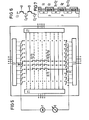
- test contacts 4 of an arrangement according to the invention for the electrical testing of microwirings are arranged in a matrix, the pitch of which corresponds to the pitch of a circuit board to be tested.
- the lines 5, 6, 15, 16, 25, 26, 36 for the test voltages embedded in the substrate 9 of an arrangement according to the invention for the electrical testing of microwirings are switched through the surface 12 at the desired points 4 via switches 2, 3, 33 3n.
- switch 2, 3, 33 is independent of the direction of the current, a switch is sufficient which either switches through the positive or negative test voltage on the one hand or is open on the other hand. In the latter case, with the switch open, the corresponding contact 4 is not involved in the measurement.
- two switches 2, 3, 33 (1 npn. And one pnp transistor) are provided for each test point 4.
- the test voltages can be switched through to the respective test contacts 4 in such a way that each test point 4 can be measured against every further test point 4.
- the respective switches or transistors 2, 3, 33, etc. done! -. tet or controlled.
- Lines 5, 15, 25 are lines with a negative test voltage
- lines 6, 16, 26, 36 are lines with a positive test voltage.
- FIG. 3 shows a schematic representation of a node of a switching matrix according to FIG. 2.
- This node belongs to a single early contact 4.
- a line 5 with a negative test potential and a line 36 with a positive early potential lead to this node according to FIG. 3 has a pnp transistor 33 and an npn transistor 2.
- the base B1 of the pnp transistor 33 is driven via the line 311.
- the base B2 of the npn transistor 2 is driven via the line 10.
- the pnp transistor 33 also has a collector K1 and an emitter E1.
- the collector K1 is identical to the line 36 in the area of the node of the switching matrix.
- the transistor 33 is turned on by driving the base B1 with a corresponding negative voltage.
- the npn transistor in Figure 3 corresponds to the transistor 2 of Figure 1 and Figure 2 and has a base B2, an emit. ter E2 and a collector K2.
- the collector K2 is identical to the power line 5. This transistor 2 is turned on when the base B2 is activated with a corresponding positive voltage.
- FIG. 4 shows a cross section through the npn transistor of FIG. 3.
- an arrangement according to the invention for the electrical testing of microwirings has a substrate SR made of pure silicon.
- an n-type semiconductor for the collector K2 and for the power line 5 is applied directly to this substrate SR.
- a p-type semiconductor for the base B2 is embedded above it.
- an n-type semiconductor for the emitter E2 is embedded therein.
- Control line 10 is arranged on one side above base B2.
- control lines 10 and 311 are insulated from air.
- a metallic contact M is applied to the emitter E2 in the example according to FIG. 4, which together with a metallic contact applied to the emitter E1 of the pnp transistor defines exactly one test contact 4 of an arrangement according to the invention for the electrical testing of microwirings.
- the area available for the test contact 4 is somewhat less than that specified by the grid dimension of an arrangement according to the invention according to FIG. 2.
- An arrangement according to Fig. 4 with two deep-set metallic contacts M above the emitter E1 and above the emitter E2 enables a soft contact on the test contact 4 via a conductive liquid, e.g.
- each test point with the coordinates X n , Y has a pair S (X n Y m ) of switches.
- the test points X 1 Y 1 and X 2 Y 2 are supplied with voltage in that all similar switches of the switch pairs S (X n Y m ) correspond to the voltages to be tested up to Y 1 and Y 2 by the row decoders Z 1 , Z 2 getting closed.
- the column decoders S 1 , S 2 then select the columns X 1 and X 2 .
- the test voltage of the DC voltage source 7 is applied to the selected test contacts X 1 Y 1 , X 2 Y 2 .
- FIG. 6 shows a possible implementation for the switches S (X n Y m ) using bipolar transistors. Similar npn transistors are connected in series in FIG. 6, the emitter E i being connected to the collector C i ⁇ 1 of the following transistor. The transistors of FIG. 6 are controlled by the row decoders Z 1 , Z 2 via the respective base contacts B.
- FIG. 7 shows a possible implementation for the switches S (X n Y m ) of FIG. 5 using MOS transistors.
- npn transistors are in turn connected, the drain electrode D i of a transistor being connected to the source electrode S i + 1 of the following transistor. stors matches.
- the row decoders Z 1 , Z 2 control these transistors via the gate electrodes G i
- a test plate according to the invention must always be aligned with the test object before the test begins.
- Representations of special transistors or layouts in the images do not limit the application of the invention to the exemplary embodiments shown.
- the switches arranged in a switching matrix can also be implemented in other ways.
Landscapes
- Engineering & Computer Science (AREA)
- Physics & Mathematics (AREA)
- General Physics & Mathematics (AREA)
- Computer Hardware Design (AREA)
- Microelectronics & Electronic Packaging (AREA)
- General Engineering & Computer Science (AREA)
- Tests Of Electronic Circuits (AREA)
- Catching Or Destruction (AREA)
- Testing Of Individual Semiconductor Devices (AREA)
- Testing Of Short-Circuits, Discontinuities, Leakage, Or Incorrect Line Connections (AREA)
Applications Claiming Priority (2)
| Application Number | Priority Date | Filing Date | Title |
|---|---|---|---|
| DE3235119 | 1982-09-22 | ||
| DE19823235119 DE3235119A1 (de) | 1982-09-22 | 1982-09-22 | Anordnung fuer die pruefung von mikroverdrahtungen und verfahren zu ihrem betrieb |
Publications (2)
| Publication Number | Publication Date |
|---|---|
| EP0107771A1 true EP0107771A1 (fr) | 1984-05-09 |
| EP0107771B1 EP0107771B1 (fr) | 1986-03-12 |
Family
ID=6173883
Family Applications (1)
| Application Number | Title | Priority Date | Filing Date |
|---|---|---|---|
| EP83109002A Expired EP0107771B1 (fr) | 1982-09-22 | 1983-09-12 | Dispositif pour examiner des montages d'éléments de microcircuit et son procédé de mise en oeuvre |
Country Status (4)
| Country | Link |
|---|---|
| US (1) | US4587481A (fr) |
| EP (1) | EP0107771B1 (fr) |
| JP (1) | JPS5975163A (fr) |
| DE (2) | DE3235119A1 (fr) |
Cited By (7)
| Publication number | Priority date | Publication date | Assignee | Title |
|---|---|---|---|---|
| EP0216135A1 (fr) * | 1985-09-04 | 1987-04-01 | Siemens Aktiengesellschaft | Dispositif pour tester le fonctionnement électrique des interconnexions des circuits électriques, en particulier des circuits imprimés |
| EP0218058A1 (fr) * | 1985-09-04 | 1987-04-15 | Siemens Aktiengesellschaft | Procédé pour tester le fonctionnement électrique de plage de connexion, en particulier d'un circuit imprimé |
| EP0239251A3 (en) * | 1986-03-27 | 1988-07-27 | Northern Telecom Limited | Method and apparatus for monitoring electromagnetic emission levels |
| EP0322607A3 (en) * | 1987-12-21 | 1989-07-19 | Siemens Aktiengesellschaft Berlin Und Munchen | Control device for an apparatus for testing electrical function of wiring patterns |
| EP0414378A3 (en) * | 1989-07-21 | 1991-09-18 | Nippon Steel Corporation | An adapter for integrated circuit elements and a method using the adapter for testing assembled elements |
| EP0639777A1 (fr) * | 1993-08-21 | 1995-02-22 | Hewlett-Packard Company | Inspection des composants électriques utilisant une sonde |
| CN106199091A (zh) * | 2016-07-22 | 2016-12-07 | 京东方科技集团股份有限公司 | 电学功能测试装置、系统及方法 |
Families Citing this family (14)
| Publication number | Priority date | Publication date | Assignee | Title |
|---|---|---|---|---|
| GB8432533D0 (en) * | 1984-12-21 | 1985-02-06 | Plessey Co Plc | Integrated circuits |
| US4949035A (en) * | 1989-01-06 | 1990-08-14 | Digital Equipment Corporation | Connector alignment verification and monitoring system |
| US5633596A (en) * | 1994-01-11 | 1997-05-27 | Key Solutions Ltd. | Fixtureless automatic test equipment and a method for registration for use therewith |
| US5781021A (en) * | 1994-01-11 | 1998-07-14 | Key Solutions Ltd. | Universal fixtureless test equipment |
| US5486766A (en) * | 1994-05-20 | 1996-01-23 | Intel Corporation | Method for testing switch matrices |
| US6067633A (en) * | 1998-03-31 | 2000-05-23 | International Business Machines Corp | Design and methodology for manufacturing data processing systems having multiple processors |
| US6343369B1 (en) * | 1998-09-15 | 2002-01-29 | Microconnect, Inc. | Methods for making contact device for making connection to an electronic circuit device and methods of using the same |
| DE19843435C2 (de) * | 1998-09-22 | 2000-08-10 | Siemens Ag | Burn-In-Testvorrichtung |
| WO2002027338A2 (fr) * | 2000-09-28 | 2002-04-04 | Koninklijke Philips Electronics N.V. | Dispositif d'essai de contacts |
| US7499354B2 (en) * | 2005-11-08 | 2009-03-03 | Texas Instruments Incorporated | Method for testing transistors having an active region that is common with other transistors and a testing circuit for accomplishing the same |
| US7982468B2 (en) * | 2008-03-13 | 2011-07-19 | Oracle America, Inc. | Apparatus and method for testing electrical interconnects with switches |
| JP5503255B2 (ja) * | 2009-11-10 | 2014-05-28 | グローバル・オーエルイーディー・テクノロジー・リミテッド・ライアビリティ・カンパニー | 画素回路、表示装置および検査方法 |
| JP5726512B2 (ja) * | 2010-12-28 | 2015-06-03 | 日置電機株式会社 | コンタクト装置、測定システムおよび検査システム |
| US12190303B2 (en) * | 2017-02-28 | 2025-01-07 | Walmart Apollo, Llc | Point-of-sale system automated testing |
Citations (2)
| Publication number | Priority date | Publication date | Assignee | Title |
|---|---|---|---|---|
| US4114093A (en) * | 1976-12-17 | 1978-09-12 | Everett/Charles, Inc. | Network testing method and apparatus |
| US4138186A (en) * | 1977-07-22 | 1979-02-06 | Everett/Charles, Inc. | Test apparatus |
Family Cites Families (14)
| Publication number | Priority date | Publication date | Assignee | Title |
|---|---|---|---|---|
| US3590369A (en) * | 1969-02-14 | 1971-06-29 | British Aircraft Corp Ltd | Switching means for automatic testing equipment |
| US3679970A (en) * | 1970-04-22 | 1972-07-25 | Automatic Elect Lab | Selection matrix including a diode test circuit |
| US3713019A (en) * | 1971-08-05 | 1973-01-23 | Gte Automatic Electric Lab Inc | Electronic scanpoint matrix having means for detecting electrical failures therein |
| GB1399006A (en) * | 1972-03-28 | 1975-06-25 | Int Computers Ltd | Circuit boards |
| US3746973A (en) * | 1972-05-05 | 1973-07-17 | Ibm | Testing of metallization networks on insulative substrates supporting semiconductor chips |
| US3803483A (en) * | 1972-05-05 | 1974-04-09 | Ibm | Semiconductor structure for testing of metallization networks on insulative substrates supporting semiconductor chips |
| US3801910A (en) * | 1972-07-03 | 1974-04-02 | Ibm | Externally accessing mechanical difficult to access circuit nodes using photo-responsive conductors in integrated circuits |
| US3806800A (en) * | 1972-12-26 | 1974-04-23 | Ibm | Method and apparatus for determining the location of electrically conductive members on a structure |
| US3851161A (en) * | 1973-05-07 | 1974-11-26 | Burroughs Corp | Continuity network testing and fault isolating |
| US3825824A (en) * | 1973-06-01 | 1974-07-23 | Gte Automatic Electric Lab Inc | Matrix scanning circuit for testing a multiplicity of circuit paths |
| DE2630993C3 (de) * | 1976-07-09 | 1979-12-06 | Siemens Ag, 1000 Berlin Und 8000 Muenchen | Schaltmatrix mit Anschlußmoduln |
| AU530415B2 (en) * | 1978-06-02 | 1983-07-14 | International Standard Electric Corp. | Integrated circuits |
| GB2029032B (en) * | 1978-08-25 | 1982-12-22 | Racal Automation Ltd | Circuit testing apparatus |
| US4471298A (en) * | 1981-12-11 | 1984-09-11 | Cirdyne, Inc. | Apparatus for automatically electrically testing printed circuit boards |
-
1982
- 1982-09-22 DE DE19823235119 patent/DE3235119A1/de not_active Withdrawn
-
1983
- 1983-06-16 US US06/504,742 patent/US4587481A/en not_active Expired - Fee Related
- 1983-09-12 EP EP83109002A patent/EP0107771B1/fr not_active Expired
- 1983-09-12 DE DE8383109002T patent/DE3362548D1/de not_active Expired
- 1983-09-16 JP JP58171034A patent/JPS5975163A/ja active Pending
Patent Citations (2)
| Publication number | Priority date | Publication date | Assignee | Title |
|---|---|---|---|---|
| US4114093A (en) * | 1976-12-17 | 1978-09-12 | Everett/Charles, Inc. | Network testing method and apparatus |
| US4138186A (en) * | 1977-07-22 | 1979-02-06 | Everett/Charles, Inc. | Test apparatus |
Cited By (14)
| Publication number | Priority date | Publication date | Assignee | Title |
|---|---|---|---|---|
| US4777432A (en) * | 1985-09-04 | 1988-10-11 | Siemens Aktiengesellschaft | Device for electrically checking printed circuit boards |
| EP0218058A1 (fr) * | 1985-09-04 | 1987-04-15 | Siemens Aktiengesellschaft | Procédé pour tester le fonctionnement électrique de plage de connexion, en particulier d'un circuit imprimé |
| EP0216135A1 (fr) * | 1985-09-04 | 1987-04-01 | Siemens Aktiengesellschaft | Dispositif pour tester le fonctionnement électrique des interconnexions des circuits électriques, en particulier des circuits imprimés |
| US5006788A (en) * | 1986-03-27 | 1991-04-09 | Northern Telecom Limited | Method and apparatus for monitoring electromagnetic emission levels |
| EP0239251A3 (en) * | 1986-03-27 | 1988-07-27 | Northern Telecom Limited | Method and apparatus for monitoring electromagnetic emission levels |
| EP0322607A3 (en) * | 1987-12-21 | 1989-07-19 | Siemens Aktiengesellschaft Berlin Und Munchen | Control device for an apparatus for testing electrical function of wiring patterns |
| US4967149A (en) * | 1987-12-21 | 1990-10-30 | Siemens Aktiengesellschaft | Drive device for an apparatus for electrical function testing of wiring matrices |
| EP0414378A3 (en) * | 1989-07-21 | 1991-09-18 | Nippon Steel Corporation | An adapter for integrated circuit elements and a method using the adapter for testing assembled elements |
| US5150047A (en) * | 1989-07-21 | 1992-09-22 | Nippon Steel Corporation | Member for use in assembly of integrated circuit elements and a method of testing assembled integrated circuit elements |
| EP0639777A1 (fr) * | 1993-08-21 | 1995-02-22 | Hewlett-Packard Company | Inspection des composants électriques utilisant une sonde |
| US5491427A (en) * | 1993-08-21 | 1996-02-13 | Hewlett-Packard Company | Probe and electrical part/circuit inspecting apparatus as well as electrical part/circuit inspecting method |
| CN106199091A (zh) * | 2016-07-22 | 2016-12-07 | 京东方科技集团股份有限公司 | 电学功能测试装置、系统及方法 |
| CN106199091B (zh) * | 2016-07-22 | 2019-05-31 | 京东方科技集团股份有限公司 | 电学功能测试装置、系统及方法 |
| US10324111B2 (en) | 2016-07-22 | 2019-06-18 | Boe Technology Group Co., Ltd. | Apparatuses, systems and methods for testing electrical functions |
Also Published As
| Publication number | Publication date |
|---|---|
| DE3235119A1 (de) | 1984-03-22 |
| EP0107771B1 (fr) | 1986-03-12 |
| US4587481A (en) | 1986-05-06 |
| JPS5975163A (ja) | 1984-04-27 |
| DE3362548D1 (en) | 1986-04-17 |
Similar Documents
| Publication | Publication Date | Title |
|---|---|---|
| EP0107771A1 (fr) | Dispositif pour examiner des montages d'éléments de microcircuit et son procédé de mise en oeuvre | |
| DE2319011C2 (de) | Verfahren zum Prüfen eines Leiternetzes auf einem isolierenden Substrat und Anordnung zur Durchführung des Verfahrens | |
| DE19581814B4 (de) | Halbleiter-Testchip mit waferintegrierter Schaltmatrix | |
| DE102017205654B4 (de) | Array-Substrat, Anzeigetafel und Steuerungsverfahren | |
| DE102014115204B4 (de) | Testen von Vorrichtungen | |
| EP0838688B1 (fr) | Appareil et procédé de test de circuits imprimés | |
| DE19801557B4 (de) | Kontakt-Prüfschaltung in einer Halbleitereinrichtung | |
| EP0382868A1 (fr) | Circuit de mesure de résistance d'échantillons | |
| DE3346158A1 (de) | Analoger festkoerperschalter | |
| DE10230716A1 (de) | Leistungsmodul | |
| DE2504076A1 (de) | Anordnung und verfahren zur kontaktpruefung von halbleiterschaltungen | |
| DE1039570B (de) | Elektronischer Umschalter zur Schaltung der Stromrichtung in einem Verbraucher | |
| DE2158270C3 (de) | Kontaktloser Schalter mit einem Feldeffekt-Thyristor | |
| DE69514606T2 (de) | Elektronenquelle mit redundanten Leitern | |
| DE19714941A1 (de) | Meßkarte und Ein/Ausgang-Anschlußtestsystem unter Verwendung derselben | |
| DE10060585A1 (de) | Vorrichtung und Verfahren zur Untersuchung einer integrierten Halbleiterschaltung | |
| EP0489052B1 (fr) | Dispositif pour le controle du fonctionnement electrique de champs de cablage, en particulier de cartes de circuits imprimes | |
| DE1901665A1 (de) | Integrierte Halbleiterschaltung in monolithischer Bauweise | |
| DE10335336B4 (de) | Feldeffektbauelemente und Kondensatoren mit Elektrodenanordnung in einer Schichtebene | |
| EP0494436A2 (fr) | Dispositif d'essai | |
| EP0286814A2 (fr) | Dispositif de commande | |
| DE1589919A1 (de) | Integrierte Schaltmatrix mit Feldeffekttransistoren | |
| DE2547938C3 (de) | Verfahren zur Prüfung von Leitungen in Geräten der Nachrichtentechnik und Schaltungsanordnung zur Durchführung des Verfahrens | |
| DE2037410C3 (de) | Zeichengenerator für ein XY-Anzeigegerät | |
| DE2254865B2 (de) | Eingangsschaltung für einen Mehremittertransistor |
Legal Events
| Date | Code | Title | Description |
|---|---|---|---|
| PUAI | Public reference made under article 153(3) epc to a published international application that has entered the european phase |
Free format text: ORIGINAL CODE: 0009012 |
|
| AK | Designated contracting states |
Designated state(s): DE FR GB NL |
|
| 17P | Request for examination filed |
Effective date: 19840524 |
|
| GRAA | (expected) grant |
Free format text: ORIGINAL CODE: 0009210 |
|
| AK | Designated contracting states |
Kind code of ref document: B1 Designated state(s): DE FR GB NL |
|
| REF | Corresponds to: |
Ref document number: 3362548 Country of ref document: DE Date of ref document: 19860417 |
|
| ET | Fr: translation filed | ||
| PLBE | No opposition filed within time limit |
Free format text: ORIGINAL CODE: 0009261 |
|
| STAA | Information on the status of an ep patent application or granted ep patent |
Free format text: STATUS: NO OPPOSITION FILED WITHIN TIME LIMIT |
|
| 26N | No opposition filed | ||
| PGFP | Annual fee paid to national office [announced via postgrant information from national office to epo] |
Ref country code: NL Payment date: 19870930 Year of fee payment: 5 |
|
| PG25 | Lapsed in a contracting state [announced via postgrant information from national office to epo] |
Ref country code: GB Effective date: 19880912 |
|
| PG25 | Lapsed in a contracting state [announced via postgrant information from national office to epo] |
Ref country code: NL Effective date: 19890401 |
|
| REG | Reference to a national code |
Ref country code: GB Ref legal event code: PCNP |
|
| NLV4 | Nl: lapsed or anulled due to non-payment of the annual fee | ||
| PG25 | Lapsed in a contracting state [announced via postgrant information from national office to epo] |
Ref country code: FR Free format text: LAPSE BECAUSE OF NON-PAYMENT OF DUE FEES Effective date: 19890531 |
|
| GBPC | Gb: european patent ceased through non-payment of renewal fee | ||
| PG25 | Lapsed in a contracting state [announced via postgrant information from national office to epo] |
Ref country code: DE Effective date: 19890601 |
|
| REG | Reference to a national code |
Ref country code: FR Ref legal event code: ST |