EP0218058A1 - Procédé pour tester le fonctionnement électrique de plage de connexion, en particulier d'un circuit imprimé - Google Patents
Procédé pour tester le fonctionnement électrique de plage de connexion, en particulier d'un circuit imprimé Download PDFInfo
- Publication number
- EP0218058A1 EP0218058A1 EP86111443A EP86111443A EP0218058A1 EP 0218058 A1 EP0218058 A1 EP 0218058A1 EP 86111443 A EP86111443 A EP 86111443A EP 86111443 A EP86111443 A EP 86111443A EP 0218058 A1 EP0218058 A1 EP 0218058A1
- Authority
- EP
- European Patent Office
- Prior art keywords
- electrode
- gas discharge
- electrodes
- collecting lines
- discharge channels
- Prior art date
- Legal status (The legal status is an assumption and is not a legal conclusion. Google has not performed a legal analysis and makes no representation as to the accuracy of the status listed.)
- Granted
Links
- 238000012360 testing method Methods 0.000 title description 22
- 238000003491 array Methods 0.000 title 1
- 239000004020 conductor Substances 0.000 claims description 17
- 102100036808 Carboxylesterase 3 Human genes 0.000 claims description 8
- 101000851624 Homo sapiens Carboxylesterase 3 Proteins 0.000 claims description 8
- 238000011990 functional testing Methods 0.000 claims description 8
- 230000005865 ionizing radiation Effects 0.000 claims description 6
- 239000012777 electrically insulating material Substances 0.000 claims description 4
- 239000000615 nonconductor Substances 0.000 claims description 2
- 239000011159 matrix material Substances 0.000 abstract description 11
- 239000007789 gas Substances 0.000 description 101
- 239000000523 sample Substances 0.000 description 10
- 238000005259 measurement Methods 0.000 description 7
- 230000004913 activation Effects 0.000 description 5
- 238000000034 method Methods 0.000 description 5
- IJGRMHOSHXDMSA-UHFFFAOYSA-N Atomic nitrogen Chemical compound N#N IJGRMHOSHXDMSA-UHFFFAOYSA-N 0.000 description 4
- 238000005516 engineering process Methods 0.000 description 4
- 239000011521 glass Substances 0.000 description 4
- 238000009413 insulation Methods 0.000 description 4
- 230000002829 reductive effect Effects 0.000 description 4
- 230000001965 increasing effect Effects 0.000 description 3
- 239000000758 substrate Substances 0.000 description 3
- 230000008901 benefit Effects 0.000 description 2
- 230000001934 delay Effects 0.000 description 2
- 239000003365 glass fiber Substances 0.000 description 2
- 239000011810 insulating material Substances 0.000 description 2
- 238000004519 manufacturing process Methods 0.000 description 2
- 239000000463 material Substances 0.000 description 2
- 229910052757 nitrogen Inorganic materials 0.000 description 2
- 239000011295 pitch Substances 0.000 description 2
- 230000008569 process Effects 0.000 description 2
- 230000005855 radiation Effects 0.000 description 2
- 230000009467 reduction Effects 0.000 description 2
- 230000003213 activating effect Effects 0.000 description 1
- 230000015572 biosynthetic process Effects 0.000 description 1
- 235000015115 caffè latte Nutrition 0.000 description 1
- 239000000919 ceramic Substances 0.000 description 1
- 230000008859 change Effects 0.000 description 1
- 230000008878 coupling Effects 0.000 description 1
- 238000010168 coupling process Methods 0.000 description 1
- 238000005859 coupling reaction Methods 0.000 description 1
- 238000002788 crimping Methods 0.000 description 1
- 230000007423 decrease Effects 0.000 description 1
- 230000003247 decreasing effect Effects 0.000 description 1
- 230000005611 electricity Effects 0.000 description 1
- 238000005530 etching Methods 0.000 description 1
- 230000006870 function Effects 0.000 description 1
- PCHJSUWPFVWCPO-UHFFFAOYSA-N gold Chemical compound [Au] PCHJSUWPFVWCPO-UHFFFAOYSA-N 0.000 description 1
- 239000010931 gold Substances 0.000 description 1
- 229910052737 gold Inorganic materials 0.000 description 1
- 230000001939 inductive effect Effects 0.000 description 1
- 230000002401 inhibitory effect Effects 0.000 description 1
- 230000003993 interaction Effects 0.000 description 1
- 150000002500 ions Chemical class 0.000 description 1
- 230000000873 masking effect Effects 0.000 description 1
- 239000012299 nitrogen atmosphere Substances 0.000 description 1
- 229910000510 noble metal Inorganic materials 0.000 description 1
- 238000005476 soldering Methods 0.000 description 1
Images


Classifications
-
- G—PHYSICS
- G01—MEASURING; TESTING
- G01R—MEASURING ELECTRIC VARIABLES; MEASURING MAGNETIC VARIABLES
- G01R1/00—Details of instruments or arrangements of the types included in groups G01R5/00 - G01R13/00 and G01R31/00
- G01R1/02—General constructional details
- G01R1/06—Measuring leads; Measuring probes
- G01R1/067—Measuring probes
- G01R1/07—Non contact-making probes
- G01R1/072—Non contact-making probes containing ionised gas
-
- G—PHYSICS
- G01—MEASURING; TESTING
- G01R—MEASURING ELECTRIC VARIABLES; MEASURING MAGNETIC VARIABLES
- G01R31/00—Arrangements for testing electric properties; Arrangements for locating electric faults; Arrangements for electrical testing characterised by what is being tested not provided for elsewhere
- G01R31/28—Testing of electronic circuits, e.g. by signal tracer
- G01R31/2801—Testing of printed circuits, backplanes, motherboards, hybrid circuits or carriers for multichip packages [MCP]
- G01R31/2805—Bare printed circuit boards
Definitions
- the invention relates to a device for the electrical functional test of wiring fields, in particular of printed circuit boards, according to the preamble of claim 1.
- the contacting of the selected measuring points is usually carried out via resilient test probes.
- the resilient test probes arranged in accordance with the grid dimension of a wiring field to be tested are fastened by means of spring sleeves which are pressed into a carrier plate and into which the test probes are inserted.
- the smallest distance between the measuring points and the current load usually determine the diameter of the resilient test probes, although 0.69 mm is mentioned as the lower limit for the diameter (Elektronik oder & educatechnik, November 1979, pages 472 and 473 ).
- a device for the electrical functional testing of wiring panels in which the hitherto usual ohm i cal contact between the measuring points is replaced by a non-contact ionic contacting via gas discharge sections.
- a plurality of gas discharge channels provided with electrodes are placed in a carrier plate which can be placed on the wiring fields, the gas discharge channels arranged in the grid of the wiring fields being open to the measuring points. If two selected measuring points are now connected to one another in an electrically conductive manner, for example by means of a conductor track, the associated gas discharge channels form two gas discharge paths which are connected in series and can be ignited by applying a sufficiently high voltage to the electrodes.
- the known device enables conductivity and insulation measurements, where very high reliability is achieved by avoiding ohm i rule contacts.
- the invention has for its object to drastically reduce the number of leads in a device of the type mentioned.
- each gas discharge channel can be equipped with at least two electrodes, the activation of one electrode alone not causing ignition and burning of gas discharges, but the activation of all electrodes is sufficient for reliable ignition and burning of gas discharges.
- the selection of a gas discharge channel equipped with preferably two electrodes according to the principle of coincidence via two electrode collecting lines can in principle be based on the fact that the ignition and / or burning of a gas discharge is only made possible by the interaction of both electrodes or that the ignition and / or burning of a gas discharge is possible one of the electrodes is prevented, this inhibitory effect being eliminated by activating this electrode.
- the measuring points are preferably contacted ionically, ie an electrode of the gas discharge paths is formed directly by the measuring points on the circuit board.
- an electrode of the gas discharge paths is formed directly by the measuring points on the circuit board.
- first electrodes of the gas discharge channels are connected to one another in rows via first electrode collecting lines and that second electrodes of the gas discharge channels are connected to one another in rows via second electrode collecting lines.
- first electrodes of the gas discharge channels are connected to one another in rows via first electrode collecting lines and that second electrodes of the gas discharge channels are connected to one another in rows via second electrode collecting lines.
- first and the second electrodes are arranged at different heights of the gas discharge channels.
- One of the electrodes can then take on the task of a grid with which the ignition of a gas discharge is controlled in a particularly reliable manner, i.e. can be prevented or initiated.
- These second electrodes can then be charged with voltage pulses which, as ignition pulses, cause the ignition of gas discharges. Otherwise, such electrodes provided with insulation have no noticeable influence on the gas discharge paths.
- a further reduction in the wiring effort results if the electrodes are formed by sections of the electrode collecting lines crossing the gas discharge channels.
- first electrode collecting lines and the second electrode collecting lines are arranged crossing one another, preferably crossing at an angle of 45 °.
- This measure takes into account the fact that two selected measuring points cannot be addressed via a common electrode bus. In an intersecting arrangement of the electrode bus line can then be safely detected by a rotation of the entire support plate by an angle of 90 ° or 270 0 relative to the wiring all measuring points.
- the safety and reliability of the device is further increased. If the distance between the first and second electrodes is small, no ionization takes place or so few ions are generated that an undesired gas discharge between the first and second electrodes cannot ignite. In this regard, it has proven to be particularly advantageous if the ratio of the distance between the first electrode and the second electrode to the distance between the second electrode and the assigned measuring point is at least 1:10.
- the probability of ignition becomes a gas discharge between the two electrodes is further reduced.
- the distance between the two electrodes can then be made particularly small.
- the electrode collecting lines are in the form of a band, their manufacture and laying can be further simplified using methods which have been tried and tested in the field of circuit technology.
- the electrode collecting lines can then be formed by the conductor tracks of a layer circuit.
- a particularly high level of functional reliability is achieved if a voltage can be applied to the first electrodes of second selected gas discharge channels via the assigned first electrode collecting lines, which voltage corresponds to at least twice the ignition voltage of a gas discharge path and if the second electrodes of the two gas discharge channels are connected via the assigned second electrode
- Such lines can be applied to the collecting lines, by means of which ignition of the gas discharge paths can be initiated.
- the second electrode collecting lines leading to the second electrodes of selected gas discharge channels all of the second electrode collecting lines can be connected to one another. This measure ensures the formation of a potential shield by the second electrodes even if not all of the electrode collecting lines intersect.
- the dimensions of the carrier plate can then be adapted to the dimensions of a testing PCB can be precisely matched.
- the interconnected second electrode collecting lines can also be connected to a potential which prevents the gas discharge lines from igniting.
- all gas discharge channels can also be exposed to ionizing radiation.
- ionizing radiation for example UV radiation, avoids ignition delays, i.e. the safety and speed of an electrical functional test can be further increased.
- Figure 1 shows a highly simplified schematic representation of the operation of a device for the electrical functional test of printed circuit boards on the basis of a non-contact ionic contact.
- a part of a circuit board labeled Lpl can be seen, on the upper side of which the ends of a conductor track Lbl form measuring points M1 and M2.
- a carrier plate Tpl made of an insulating material, such as glass, is placed on the top of the printed circuit board Lpl, and a plurality of gas discharge channels are introduced in the form of blind holes.
- Gkl assigned to the measuring point M1
- Gk2 assigned to the measuring point M2 are shown.
- Electrodes E1 and E2 are arranged on the side of the gas discharge channel Gkl opposite the measuring point M1, the electrode E2 being somewhat lower than the electrode El.
- the electrode E1 is connected to an electrode manifold ES1 and the electrode E2 to an electrode manifold ES2.
- electrodes E3 and E4 are arranged on the side of the gas discharge channel Gk2 opposite the measuring point M2, the electrode E4 again being somewhat lower, ie at the same height as the electrode E2.
- the electrode E3 is connected to an electrode collecting line ES3, while the electrode E4 is connected to an electrode collecting line ES4.
- the electrodes of a multiplicity of gas discharge channels (not shown in FIG.
- the activation of the first electrodes E1 and E3 described above is not sufficient for a clear selection of the measuring points M1 and M2.
- the second electrodes E2 and E4 of the associated gas discharge channels Gkl and Gk2 are simultaneously controlled via the electrode collecting lines ES2 and ES4, according to the principle of coincidence, this control being indicated by switches S2 and S4.
- a voltage source Sq2 and a series resistor Vw2 are arranged in series between the switches S2 and S4.
- the entire arrangement shown in FIG. 1 is located in an evacuable space under a reduced pressure of, for example, 10 torr, the evacuable space being filled with a gas such as nitrogen.
- a gas such as nitrogen.
- the voltage of the voltage source Sql is now dimensioned such that at least twice the ignition voltage Uz of a gas discharge line is applied to these two gas discharge lines connected in series via the switches S1 and S3.
- the gas discharges once ignited can then no longer be influenced by the second electrodes E2 and E4, which act as a grid.
- the burning of the two gas discharges can be registered via the current measuring device Sm which is switched into the circuit.
- Figure 2 shows a variant in which the carrier plate with TplO and the assigned to the measuring points M1 and M2 ten gas discharge channels are designated Gk 10 and Gkll.
- the control of the first electrodes E10 and E12 takes place in the manner described above via the switches S1 and S3 and corresponding first electrode bus lines ES10 and ES12.
- the voltage source Sql is set to a voltage which is at least twice the operating voltage Ub one Corresponds to gas discharge path, but does not reach twice the ignition voltage Uz.
- the second electrodes of the gas discharge channels Gk10 and Gkll, denoted by Ell and E13, are controlled via assigned electrode collecting lines ES10 or ES13 and switches S11 and S13.
- the two second electrodes E11 and E13 are connected to a pulse generator Ie, via which a high-voltage pulse HI of opposite polarity can be applied simultaneously to ignite gas discharges.
- a negative high-voltage pulse HI is applied to the second electrode Ell, while a positive high-voltage pulse HI is applied to the second electrode E13 at the same time.
- the high-voltage pulses HI which are significantly larger than the ignition voltage Uz, can also reliably ignite the gas discharges if the second electrodes Ell and E13 are coated with an electrically insulating material M, e.g. a ceramic, are covered.
- the covering with the electrically insulating material M has the advantage that the second electrodes E1 and E13 act as pure ignition electrodes and do not otherwise influence the gas discharges.
- FIG. 3 shows a perspective view of a part of a printed circuit board Lp20, on the surface of which measuring points M20, M21, M22 and M23 arranged in grid spacing and conductor tracks Lb20, Lb21, Lb22, Lb23 and Lb24 can be seen.
- the main directions of the conductor tracks, which are perpendicular to one another, are designated HR1 and HR2.
- a carrier plate, generally designated Tp20 is placed, into which a plurality of cylindrical gas discharge channels Gk20 is introduced.
- the carrier plate Tp20 which is composed of an upper plate Po and a lower plate Pu, consists of shaped glass which can be structured photolithographically, into which the gas discharge channels Gk20 are introduced by means of conventional masking and etching techniques.
- the upper side of the upper plate Po there are also rectilinear grooves which run in the main direction HR2 and in which first electrode collecting lines ES21 run.
- the first electrodes of the gas discharge channels Gk20, designated E21 are formed directly by sections of the electrode collecting lines ES21 crossing the gas discharge channels Gk20.
- the second electrodes of the gas discharge channels Gk20 are formed directly by sections of the second electrode collecting lines ES20 crossing the gas discharge channels Gk20.
- the production of the band-shaped electrode collecting lines ES20 and ES21 with the associated electrodes E20 and E21 can be carried out using techniques customary in the field of printed circuits or layer circuits, the materials used being noble metals such as e.g. Gold are suitable.
- the position of the gas discharge channels Gk20 corresponds exactly to the grid of the measuring points of a circuit board Lp20 to be tested, with the precise assignment of gas discharge channels Gk20 lying in the sectional plane of the carrier plate Tp20 to the measuring points M20, M21, M22 and M23 located directly underneath being clearly recognizable is. It can also be seen that the number of gas discharge channels Gk20 arranged in rows and columns may well be greater than the number of measuring points present on the circuit board Lp20.
- the thickness of the upper plate Po is greatly exaggerated in Figure 3.
- the thickness of the upper plate Po is very small in relation to the thickness of the lower plate Pu, so that the distance between the first electrode E21 and the second electrode E20 of a gas discharge channel Gk20 is also small in relation to the distance between the second electrode E20 and an assigned measuring point.
- This measurement reliably prevents undesired gas discharges between a first electrode E21 and a second electrode E20.
- a cover plate made of insulating material is additionally placed on top of the upper plate Po.
- this cover plate is made of glass, so that all gas discharge channels Gk20 can be subjected to ionizing radiation iS, which is only indicated by arrows.
- This ionizing radiation iS which is, for example, UV radiation, avoids ignition delays and increases the safety and speed of the electrical function test.
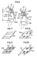
- FIG. 4 shows the principle of matrix addressing selected measuring points of the device shown in Figure 3 in a highly simplified schematic representation.
- the top view shows 6x6 gas discharge channels Gk20, which are traversed by the associated electrode collecting lines ES20 and ES21.
- measuring points M200 and M201 are activated in the manner described in FIG. 1. In this control, which is only indicated by arrows in FIG.
- the matrix addressing described above with reference to FIG. 4 only fails if the same first electrode bus line ES21 or the same second electrode bus line ES20 is assigned to the selected measuring points or gas discharge channels Gk20. This case is shown in FIG. 4 by measuring points M202 and M203, which are to be connected to one another by a dashed line Lb201 and to which the same first electrode bus line ES21 is assigned. The matrix addressing of these measuring points M202 and M203 or the testing of the conductor track Lb201 is shown in FIG. 5.
- a second device which has been appropriately designed from the outset can also be used to record all measuring points.
- FIG. 6 shows a highly simplified schematic illustration of a first variant of the arrangement of the first and second electrodes of the gas discharge channels. Only the contour of the gas discharge channels Gk30 introduced into a carrier plate composed of two layers can be seen.
- the first electrode collecting lines ES31 which form the first electrodes E31, run in a groove N1.
- the second electrode collecting lines ES30 which form the second electrodes E30, run in a groove N2.
- the distance a between the l first electrode bus lines ES30 and the second electrode bus lines ES31, which intersect at an angle of 45 °, is defined by electrically insulating glass fibers Gf, which is also in the grooves N1 are laid.
- the ratio of the distance a between a first electrode E31 and a second electrode E30 to the distance d between a second electrode E30 and an associated measuring point M30 is so small that no gas discharges can ignite between the first electrodes E31 and the second electrodes E30. This is guaranteed with certainty if the ratio a: d is at least 1:10.
- Figures 7 to 10 show different stages of the process for the arrangement of the first and second electrodes according to a second variant.
- conductor tracks using thick-film technology are first applied to a substrate Su made of glass, these conductor tracks forming parallel first electrode collecting lines ES41.
- a first insulating layer Isl is then applied over the entire surface, which only in the form of windows does not cover those areas of the first electrode collecting lines ES41 which form the first electrodes E41.
- further conductor tracks are then applied to the first insulating layer Isl using thick-film technology, these conductor tracks forming parallel second electrode collecting lines ES40 and crossing the first electrode collecting lines ES41 at an angle of 45 °.
- a second insulating layer Is2 is then applied again over the entire area, which merely in the form of windows does not cover the first electrodes E41 and those regions of the second electrode collecting lines ES40 which form the second electrodes E40.
- FIG. 10 shows, only the first electrodes E41 and the second electrodes E40 are then exposed, while the entire remaining area is exposed by the second insulating layer Is2 is covered.
- the substrate Su printed in this way then only needs to be placed upside down on a carrier plate, into which gas discharge channels are introduced as through holes in a corresponding grid.
- a first electrode E41 and a second electrode E40 are then located closely next to one another and electrically insulated from one another at the upper end of each gas discharge channel.
- the grid dimension of the measuring points and thus also of the gas discharge channels Gk20 is, for example, 1/40 ", ie approximately 0.6 mm.
- the diameter of the gas discharge channels Gk20 is then 0.3 mm and that is approximately the thickness of the whole Support ') latte Tp20 corresponding distance e between the first electrodes E21 and the assigned measuring points 0.5 mm.
- the entire arrangement is at a reduced pressure p of about 10 Torr in a nitrogen atmosphere.
- Gas discharge channels Gk20 leading second electrode collecting lines ES20 a voltage is applied which is at least twice the burner voltage corresponds and is, for example, 650 volts.
Landscapes
- Engineering & Computer Science (AREA)
- Physics & Mathematics (AREA)
- General Physics & Mathematics (AREA)
- Computer Hardware Design (AREA)
- Microelectronics & Electronic Packaging (AREA)
- General Engineering & Computer Science (AREA)
- Testing Relating To Insulation (AREA)
- Testing Of Short-Circuits, Discontinuities, Leakage, Or Incorrect Line Connections (AREA)
- Gas-Filled Discharge Tubes (AREA)
- Glass Compositions (AREA)
Priority Applications (1)
| Application Number | Priority Date | Filing Date | Title |
|---|---|---|---|
| AT86111443T ATE52618T1 (de) | 1985-09-04 | 1986-08-19 | Vorrichtung fuer die elektrische funktionspruefung von verdrahtungsfeldern, insbesondere von leiterplatten. |
Applications Claiming Priority (2)
| Application Number | Priority Date | Filing Date | Title |
|---|---|---|---|
| DE3531604 | 1985-09-04 | ||
| DE3531604 | 1985-09-04 |
Publications (2)
| Publication Number | Publication Date |
|---|---|
| EP0218058A1 true EP0218058A1 (fr) | 1987-04-15 |
| EP0218058B1 EP0218058B1 (fr) | 1990-05-09 |
Family
ID=6280128
Family Applications (1)
| Application Number | Title | Priority Date | Filing Date |
|---|---|---|---|
| EP86111443A Expired - Lifetime EP0218058B1 (fr) | 1985-09-04 | 1986-08-19 | Procédé pour tester le fonctionnement électrique de plage de connexion, en particulier d'un circuit imprimé |
Country Status (5)
| Country | Link |
|---|---|
| US (1) | US4777432A (fr) |
| EP (1) | EP0218058B1 (fr) |
| JP (1) | JPS6256872A (fr) |
| AT (1) | ATE52618T1 (fr) |
| DE (1) | DE3671106D1 (fr) |
Cited By (6)
| Publication number | Priority date | Publication date | Assignee | Title |
|---|---|---|---|---|
| EP0322607A3 (en) * | 1987-12-21 | 1989-07-19 | Siemens Aktiengesellschaft Berlin Und Munchen | Control device for an apparatus for testing electrical function of wiring patterns |
| US4897598A (en) * | 1987-03-31 | 1990-01-30 | Siemens Aktiengesellschaft | Apparatus for electrical function testing of wiring matrices, particularly of printed circuit boards |
| EP0409398A3 (en) * | 1989-06-26 | 1992-02-26 | Digital Equipment Corporation | Test cell for non-contact testing of electrical circuits for open/short circuiting |
| WO1999056137A1 (fr) * | 1998-04-27 | 1999-11-04 | Exsight Electro-Optical Systems Ltd. | Procede et appareil de test de reseaux d'interconnexion |
| WO1999056136A1 (fr) * | 1998-04-27 | 1999-11-04 | Exsight Electro-Optical Systems Ltd. | Procede et appareil permettant de tester des reseaux d'interconnexion au moyen de courants electriques guides |
| WO2010040161A3 (fr) * | 2008-10-07 | 2010-07-01 | Nanoldent Technologies Ag | Dispositif de commutation pour tester des contacts électriques |
Families Citing this family (7)
| Publication number | Priority date | Publication date | Assignee | Title |
|---|---|---|---|---|
| EP0285798A3 (fr) * | 1987-03-31 | 1990-03-07 | Siemens Aktiengesellschaft | Dispositif de test électrique du fonctionnement de rangées de fils électriques, en particulier pour cartes de circuit |
| DE3927842A1 (de) * | 1989-08-23 | 1991-02-28 | Siemens Ag | Vorrichtung fuer die elektrische funktionspruefung von verdrahtungsfeldern, insbesondere von leiterplatten |
| JPH07140209A (ja) * | 1993-09-20 | 1995-06-02 | Fujitsu Ltd | 回路配線基板の検査装置およびその検査方法 |
| US5570027A (en) * | 1995-04-19 | 1996-10-29 | Photocircuits Corporation | Printed circuit board test apparatus and method |
| US5587664A (en) * | 1995-07-12 | 1996-12-24 | Exsight Ltd. | Laser-induced metallic plasma for non-contact inspection |
| US6118285A (en) * | 1998-01-28 | 2000-09-12 | Probot, Inc | Non-contact plasma probe for testing electrical continuity of printed wire boards |
| US8643380B1 (en) * | 2010-07-15 | 2014-02-04 | Edward Herbert | Method and apparatus for reducing shock and arc-flash hazards in power distribution systems |
Citations (2)
| Publication number | Priority date | Publication date | Assignee | Title |
|---|---|---|---|---|
| EP0102565A2 (fr) * | 1982-08-25 | 1984-03-14 | Siemens Aktiengesellschaft | Méthode et dispositif pour tester électriquement des micro-câblages |
| EP0107771A1 (fr) * | 1982-09-22 | 1984-05-09 | Siemens Aktiengesellschaft | Dispositif pour examiner des montages d'éléments de microcircuit et son procédé de mise en oeuvre |
Family Cites Families (5)
| Publication number | Priority date | Publication date | Assignee | Title |
|---|---|---|---|---|
| US3800296A (en) * | 1972-04-26 | 1974-03-26 | Univ Illinois | Optical write-in method and apparatus for a plasma display panel |
| US3946381A (en) * | 1972-06-05 | 1976-03-23 | National Science Foundation | Graphic system apparatus utilizing plasma display/memory devices with direct electrical read-out |
| JPH0127432B2 (fr) * | 1975-01-24 | 1989-05-29 | Hitachi Ltd | |
| DE2508393C2 (de) * | 1975-02-26 | 1983-02-17 | Siemens AG, 1000 Berlin und 8000 München | Gasentladungsanzeigevorrichtung und Verfahren zu ihrem Betrieb |
| CA1048182A (fr) * | 1976-10-26 | 1979-02-06 | Her Majesty The Queen, In Right Of Canada, As Represented By The Minister Of National Defence | Affichage au plasma commande par laser |
-
1986
- 1986-08-19 DE DE8686111443T patent/DE3671106D1/de not_active Expired - Lifetime
- 1986-08-19 EP EP86111443A patent/EP0218058B1/fr not_active Expired - Lifetime
- 1986-08-19 AT AT86111443T patent/ATE52618T1/de not_active IP Right Cessation
- 1986-09-01 JP JP61205747A patent/JPS6256872A/ja active Pending
- 1986-09-02 US US06/902,925 patent/US4777432A/en not_active Expired - Fee Related
Patent Citations (2)
| Publication number | Priority date | Publication date | Assignee | Title |
|---|---|---|---|---|
| EP0102565A2 (fr) * | 1982-08-25 | 1984-03-14 | Siemens Aktiengesellschaft | Méthode et dispositif pour tester électriquement des micro-câblages |
| EP0107771A1 (fr) * | 1982-09-22 | 1984-05-09 | Siemens Aktiengesellschaft | Dispositif pour examiner des montages d'éléments de microcircuit et son procédé de mise en oeuvre |
Non-Patent Citations (1)
| Title |
|---|
| IBM TECHNICAL DISCLOSURE BULLETIN, Band 14, Nr. 5, Oktober 1971, Seite 1601, New York, US; H. BOHLEN et al.: "Tester for electric conductors" * |
Cited By (10)
| Publication number | Priority date | Publication date | Assignee | Title |
|---|---|---|---|---|
| US4897598A (en) * | 1987-03-31 | 1990-01-30 | Siemens Aktiengesellschaft | Apparatus for electrical function testing of wiring matrices, particularly of printed circuit boards |
| EP0285799A3 (en) * | 1987-03-31 | 1990-03-28 | Siemens Aktiengesellschaft | Device for the functional electric testing of wiring arrays, in particular of circuit boards |
| US4967148A (en) * | 1987-03-31 | 1990-10-30 | Siemens Aktiengesellschaft | Apparatus for electrical function testing of wiring matrices, particularly of printed circuit boards |
| EP0322607A3 (en) * | 1987-12-21 | 1989-07-19 | Siemens Aktiengesellschaft Berlin Und Munchen | Control device for an apparatus for testing electrical function of wiring patterns |
| US4967149A (en) * | 1987-12-21 | 1990-10-30 | Siemens Aktiengesellschaft | Drive device for an apparatus for electrical function testing of wiring matrices |
| EP0409398A3 (en) * | 1989-06-26 | 1992-02-26 | Digital Equipment Corporation | Test cell for non-contact testing of electrical circuits for open/short circuiting |
| WO1999056137A1 (fr) * | 1998-04-27 | 1999-11-04 | Exsight Electro-Optical Systems Ltd. | Procede et appareil de test de reseaux d'interconnexion |
| WO1999056136A1 (fr) * | 1998-04-27 | 1999-11-04 | Exsight Electro-Optical Systems Ltd. | Procede et appareil permettant de tester des reseaux d'interconnexion au moyen de courants electriques guides |
| WO2010040161A3 (fr) * | 2008-10-07 | 2010-07-01 | Nanoldent Technologies Ag | Dispositif de commutation pour tester des contacts électriques |
| US9958478B2 (en) | 2008-10-07 | 2018-05-01 | Asmag-Holding Gmbh | Switching apparatus for electrical contact testing |
Also Published As
| Publication number | Publication date |
|---|---|
| US4777432A (en) | 1988-10-11 |
| DE3671106D1 (de) | 1990-06-13 |
| JPS6256872A (ja) | 1987-03-12 |
| ATE52618T1 (de) | 1990-05-15 |
| EP0218058B1 (fr) | 1990-05-09 |
Similar Documents
| Publication | Publication Date | Title |
|---|---|---|
| EP0285799B1 (fr) | Dispositif de test électrique du fonctionnement de rangées de fils électriques, en particulier pour cartes de circuit | |
| DE2360801C2 (de) | Schaltungsprüfeinrichtung für integrierte Schaltkreise auf Schichtschaltungsträgern | |
| EP0218058B1 (fr) | Procédé pour tester le fonctionnement électrique de plage de connexion, en particulier d'un circuit imprimé | |
| EP0263244B1 (fr) | Dispositif de test électronique pour circuits imprimés à pointes de contact disposées en trame extrêmement fine (1/20 à 1/10 de pouce) | |
| DE4231185C2 (de) | Prüfelektrodeneinheit für gedruckte Leiterplatten sowie Prüfgerät mit einer solchen Prüfelektrodeneinheit | |
| EP0216135B1 (fr) | Dispositif pour tester le fonctionnement électrique des interconnexions des circuits électriques, en particulier des circuits imprimés | |
| DE2319011A1 (de) | Verfahren zum eektrischen pruefen eines chips untereinander verbindenden leiternetzes auf einem substrat | |
| EP0838688B1 (fr) | Appareil et procédé de test de circuits imprimés | |
| DE2744299C2 (de) | Verfahren zum elektrischen Prüfen eines Leiterbahnmusters auf einem Substrat | |
| EP0250620B1 (fr) | Procédé et dispositif pour tester électriquement des circuits imprimés | |
| EP1057038A1 (fr) | Procede et dispositif pour le test de cartes imprimees | |
| DE2137619A1 (de) | Verfahren zum pruefen des elektrischen durchganges | |
| EP0142119A1 (fr) | Dispositif pour adapter le pas d'une grille de contact d'un appareil de contrôle de circuits imprimés | |
| EP0285798A2 (fr) | Dispositif de test électrique du fonctionnement de rangées de fils électriques, en particulier pour cartes de circuit | |
| EP0102565A2 (fr) | Méthode et dispositif pour tester électriquement des micro-câblages | |
| EP0322607B1 (fr) | Appareil de commande pour un dispositif pour le test de platines de circuits | |
| EP0875767B1 (fr) | Appareil et procédé pour tester des circuits imprimés non pourvus de composants | |
| EP0489052B1 (fr) | Dispositif pour le controle du fonctionnement electrique de champs de cablage, en particulier de cartes de circuits imprimes | |
| DE2655841C3 (de) | Integrierter Widerstandsbaustein zum Einlöten in eine Flachbaugruppe | |
| EP0286814A2 (fr) | Dispositif de commande | |
| EP0068493B1 (fr) | Assemblage de sondes d'essai pour circuits intégrés | |
| EP0181429A1 (fr) | Fiche de contact | |
| DE8515436U1 (de) | Kontaktstift aus elektrisch leitendem Werkstoff zu Verwendung in einer elektrischen Prüfvorrichtung für Leiterplatten | |
| DE2752749C3 (de) | Kontaktiervorrichtung | |
| DE2331278C3 (de) | Gasentladungs-Anzeigetafel |
Legal Events
| Date | Code | Title | Description |
|---|---|---|---|
| PUAI | Public reference made under article 153(3) epc to a published international application that has entered the european phase |
Free format text: ORIGINAL CODE: 0009012 |
|
| AK | Designated contracting states |
Kind code of ref document: A1 Designated state(s): AT BE CH DE FR GB IT LI NL SE |
|
| 17P | Request for examination filed |
Effective date: 19870506 |
|
| 17Q | First examination report despatched |
Effective date: 19890217 |
|
| GRAA | (expected) grant |
Free format text: ORIGINAL CODE: 0009210 |
|
| AK | Designated contracting states |
Kind code of ref document: B1 Designated state(s): AT BE CH DE FR GB IT LI NL SE |
|
| REF | Corresponds to: |
Ref document number: 52618 Country of ref document: AT Date of ref document: 19900515 Kind code of ref document: T |
|
| REF | Corresponds to: |
Ref document number: 3671106 Country of ref document: DE Date of ref document: 19900613 |
|
| ET | Fr: translation filed | ||
| ITF | It: translation for a ep patent filed | ||
| GBT | Gb: translation of ep patent filed (gb section 77(6)(a)/1977) | ||
| PLBE | No opposition filed within time limit |
Free format text: ORIGINAL CODE: 0009261 |
|
| STAA | Information on the status of an ep patent application or granted ep patent |
Free format text: STATUS: NO OPPOSITION FILED WITHIN TIME LIMIT |
|
| 26N | No opposition filed | ||
| PGFP | Annual fee paid to national office [announced via postgrant information from national office to epo] |
Ref country code: AT Payment date: 19910726 Year of fee payment: 6 |
|
| PGFP | Annual fee paid to national office [announced via postgrant information from national office to epo] |
Ref country code: SE Payment date: 19910816 Year of fee payment: 6 |
|
| PGFP | Annual fee paid to national office [announced via postgrant information from national office to epo] |
Ref country code: BE Payment date: 19910828 Year of fee payment: 6 |
|
| ITTA | It: last paid annual fee | ||
| PG25 | Lapsed in a contracting state [announced via postgrant information from national office to epo] |
Ref country code: AT Effective date: 19920819 |
|
| PG25 | Lapsed in a contracting state [announced via postgrant information from national office to epo] |
Ref country code: SE Effective date: 19920820 |
|
| PG25 | Lapsed in a contracting state [announced via postgrant information from national office to epo] |
Ref country code: BE Effective date: 19920831 |
|
| PGFP | Annual fee paid to national office [announced via postgrant information from national office to epo] |
Ref country code: CH Payment date: 19921120 Year of fee payment: 7 |
|
| BERE | Be: lapsed |
Owner name: SIEMENS A.G. Effective date: 19920831 |
|
| PG25 | Lapsed in a contracting state [announced via postgrant information from national office to epo] |
Ref country code: LI Effective date: 19930831 Ref country code: CH Effective date: 19930831 |
|
| REG | Reference to a national code |
Ref country code: CH Ref legal event code: PL |
|
| EUG | Se: european patent has lapsed |
Ref document number: 86111443.7 Effective date: 19930307 |
|
| PGFP | Annual fee paid to national office [announced via postgrant information from national office to epo] |
Ref country code: GB Payment date: 19980721 Year of fee payment: 13 |
|
| PGFP | Annual fee paid to national office [announced via postgrant information from national office to epo] |
Ref country code: NL Payment date: 19980825 Year of fee payment: 13 |
|
| PGFP | Annual fee paid to national office [announced via postgrant information from national office to epo] |
Ref country code: FR Payment date: 19980826 Year of fee payment: 13 |
|
| PGFP | Annual fee paid to national office [announced via postgrant information from national office to epo] |
Ref country code: DE Payment date: 19981020 Year of fee payment: 13 |
|
| PG25 | Lapsed in a contracting state [announced via postgrant information from national office to epo] |
Ref country code: GB Free format text: LAPSE BECAUSE OF NON-PAYMENT OF DUE FEES Effective date: 19990819 |
|
| PG25 | Lapsed in a contracting state [announced via postgrant information from national office to epo] |
Ref country code: NL Free format text: LAPSE BECAUSE OF NON-PAYMENT OF DUE FEES Effective date: 20000301 |
|
| GBPC | Gb: european patent ceased through non-payment of renewal fee |
Effective date: 19990819 |
|
| PG25 | Lapsed in a contracting state [announced via postgrant information from national office to epo] |
Ref country code: FR Free format text: LAPSE BECAUSE OF NON-PAYMENT OF DUE FEES Effective date: 20000428 |
|
| NLV4 | Nl: lapsed or anulled due to non-payment of the annual fee |
Effective date: 20000301 |
|
| PG25 | Lapsed in a contracting state [announced via postgrant information from national office to epo] |
Ref country code: DE Free format text: LAPSE BECAUSE OF NON-PAYMENT OF DUE FEES Effective date: 20000601 |
|
| REG | Reference to a national code |
Ref country code: FR Ref legal event code: ST |
|
| PG25 | Lapsed in a contracting state [announced via postgrant information from national office to epo] |
Ref country code: IT Free format text: LAPSE BECAUSE OF NON-PAYMENT OF DUE FEES;WARNING: LAPSES OF ITALIAN PATENTS WITH EFFECTIVE DATE BEFORE 2007 MAY HAVE OCCURRED AT ANY TIME BEFORE 2007. THE CORRECT EFFECTIVE DATE MAY BE DIFFERENT FROM THE ONE RECORDED. Effective date: 20050819 |