EP0108308B1 - Photo-elektrischer Umsetzungsapparat - Google Patents
Photo-elektrischer Umsetzungsapparat Download PDFInfo
- Publication number
- EP0108308B1 EP0108308B1 EP83110484A EP83110484A EP0108308B1 EP 0108308 B1 EP0108308 B1 EP 0108308B1 EP 83110484 A EP83110484 A EP 83110484A EP 83110484 A EP83110484 A EP 83110484A EP 0108308 B1 EP0108308 B1 EP 0108308B1
- Authority
- EP
- European Patent Office
- Prior art keywords
- signal
- photoelectric conversion
- time period
- pulse
- amplifier
- Prior art date
- Legal status (The legal status is an assumption and is not a legal conclusion. Google has not performed a legal analysis and makes no representation as to the accuracy of the status listed.)
- Expired
Links
Images
Classifications
-
- H—ELECTRICITY
- H04—ELECTRIC COMMUNICATION TECHNIQUE
- H04N—PICTORIAL COMMUNICATION, e.g. TELEVISION
- H04N1/00—Scanning, transmission or reproduction of documents or the like, e.g. facsimile transmission; Details thereof
- H04N1/40—Picture signal circuits
- H04N1/40056—Circuits for driving or energising particular reading heads or original illumination means
-
- H—ELECTRICITY
- H04—ELECTRIC COMMUNICATION TECHNIQUE
- H04N—PICTORIAL COMMUNICATION, e.g. TELEVISION
- H04N25/00—Circuitry of solid-state image sensors [SSIS]; Control thereof
- H04N25/60—Noise processing, e.g. detecting, correcting, reducing or removing noise
Definitions
- the present invention relates to a photoelectric conversion apparatus which includes a plurality of linearly arranged photoelectric conversion elements and is used, for example, as a linear image sensor.
- the linear image sensor used receives reflected light from an object to be read out and converts the incident light into electric signals.
- the linear image sensor includes a photoelectric conversion element array of a number of linearly arranged photoelectric conversion elements, and a circuit for reading out electric image signals from the respective photoelectric conversion elements.
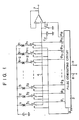
- the conventional photoelectric conversion apparatus shown in Fig. 1 includes a photoelectric conversion element array of a number of linearly arranged photoelectric conversion elements, e.g., photodiodes 1 1 to 1 n ; and a circuit device for sequentially reading out the electric image signals from the respective photodiodes.
- the circuit device includes a common output line 4; analog switches 3 1 to 3n which comprise, e.g., MOSFETs, and are respectively connected between the common output line 4 and the photodiodes 1 1 to 1 n ; and a pulse generating circuit 2 for generating scanning pulses ⁇ 1 to ⁇ n and an inhibit pulse ⁇ IN for use in controlling the ON/OFF operation of the analog switches 3 1 to 3 n .
- the sensor further includes a signal processing circuit which reads out the signals from the photodiodes 1 1 to 1 n onto the common output line 4, and then produces the signals as a video signal 7.
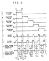
- the signal processing circuit includes a capacitor C v connected to the common output line 4 and ground; and analog switch 5 connected between the common output line 4 and ground, the ON/OFF operation of which is controlled by a clear pulse ⁇ R from the pulse generating circuit 2; and an operational amplifier 6 connected to the common output line 4. If it is assumed that only the photodiodes 1 i to 1 5 are arranged in the apparatus shown in Fig. 1, the timings of the pulses generated by the pulse generating circuit 2 and the timings of the signals read out on the common output line 4 hold the relationship shown in Fig. 2. Referring to Fig. 2, the scanning pulses ⁇ 1 to ⁇ 5 have a pulse width T and sequentially and repeatedly scan the analog switches 3 1 to 3 5 (Figs. 2A to 2E).
- each diode stores a charge in response to the project light intensity during this one line scanning time period.
- an inhibit pulse ⁇ IN (Fig. 2F) which is synchronous with the switching timing from pulse ⁇ 1 to pulse ⁇ 2 is applied to the analog switches 3 1 to 3 5 .
- the analog switches 3 1 to 3 5 are turned off.
- T1 is the rising time of the scanning pulse ⁇ 1
- T5 is the falling time thereof
- T2 is the falling time of the inhibit pulse ⁇ IN at the time T1
- T4 is the rising time of the inhibit pulse ⁇ IN corresponding to time T5
- the analog switch 3 1 is turned on from the time T2 to T4.
- charge from the photodiode 1 1 is read out onto the common output line 4 from the time T2 to T4.
- the charge is charged on the capacitor C v connected to the common output line 4.
- the charge time constant ⁇ of the capacitor C v is about 0.7C v ⁇ r where r is the ON resistance of the analog switch 3 1 .
- the pulse generating circuit 2 may comprise a shift register, or a counter which receives a start pulse 8 and clock pulses 9. For the sake of simplicity, a descripiton has been made only with reference to pulse ⁇ 1 . However, the mode of operation for the other scanning pulses ⁇ 2 to ⁇ 5 remains the same.
- the defects of the conventional photoelectric conversion apparatus shown in Fig. 1 will now be described, based on the assumption that the photodiode array only has photodiodes 1 1 to 1 5 .
- the common output line 4 receives the noise signal components a well as the image signal components based on charges stored on the photodiodes.
- the noise signal components are generated due to the turning on and turning off of the analog switches and gate capacitances of the MOS transistors constituting the analog switches. Accordingly, the noise signals differ for the respective analog switches.
- the operational amplifier 6 produces noise signals e N1 to e N5 , as shown in Fig. 2H.
- the noise signals have the varied amplitudes shown in Fig. 2H, for the reason given above.
- the case wherein uniform light is projected onto the photodiodes 1 1 to 1 5 may be described as follows. Under such conditions, the amplitudes of the image signals read out from the photodiodes 1 1 to 1 5 must be the same. However, since the corresponding noise signals are added to these image signals, the operational amplifier 6 produces the video signals e S1 to e S5 shown in Fig. 21. The ON resistances of the analog switches 3 1 to 3 5 change in accordance with the ambient temperature. Accordingly, variations in the video signals are further enhanced. When such noise signals e N1 to e N5 are generated, the photoelectric reading of, e.g., slips, becomes unreliable, and the processing of slips becomes impossible.
- a primary object of the present invention is to provide a photoelectric conversion apparatus which eliminates noise signals normally generated during the switching of analog switches, and which is capable of producing image signals from photoelectric conversion elements such as video signals.
- a photoelectric conversion apparatus comprises an array of photoelectric conversion elements, each of which produces an electric image signal component in response to a projected light; a common output line; a plurality of analog switches, each of which is connected between the common output line and the corresponding photoelectric conversion element; a pulse generating circuit which produces a plurality of scanning pulses, which pulses subsequently scan the analog switches for reading out the electric image signal comonents on the common output line, in succession, by turning ON each of the analog switches for a predetermined time period; means for turning ON an analog switch for at least a first time period and for a second time period, during a predetermined time period in which the analog switch is scanned by a scanning pulse corresponding to the analog switch; first means connected to the common output line and the pulse generating circuit, for use in obtaining a first signal produced during the first time period which first signal includes the image signal component from a photoelectric conversion element and a noise signal component, and for obtaining a second signal produced during the second time period, which second signal includes only the
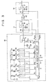
- the circuit portion surrounded by a dotted line 10 has substantially the same configuration as that of the apparatus shown in Fig. 1 but differs therefrom in that the frequency of the inhibit pulse ⁇ IN and the clear pulse ⁇ R in Fig. 3 is twice that of the apparatus shown in Fig. 1 and that the pulse generating circuit 2 generates sampling pulses ⁇ PSP1 and ⁇ SP2 .
- the 3 further includes a first sample hold circuit 11 connected to the output terminal of the operational amplifier (to be referred to as a first amplifier, hereinafter) 6 and to the output terminal of the pulse generating circuit 2; a differential amplifier 13 which receives an output signal from the first sample hold circuit 11, as well as a noise signal component from the first amplifier 6; and a second sample hold circuit 14 which receives an output signal from the differential amplifier 13 and produces an image signal component such as video signal.
- the first sample hold circuit 11 includes a second amplifier 15; an analog switch 16 which is inserted between the positive input terminal of the second amplifier 15 and the output terminal of the first amplifier 6, and which is turned on while it is receiving a sampling pulse ⁇ SP1 ; and a capacitor 12 connected between the positive input terminal of the second amplifier 15 and ground.
- the negative input terminal of the second amplifier 15 and the output terminal of the sample hold circuit 11 are connected to each other.
- the second sample hold circuit 14 includes a third amplifier 17, another analog switch 18 which is inserted between the positive input terminal of the third amplifier 17 and the output terminal of the differential amplifier 13 and which is turned on while it is receiving a sampling pulse ⁇ PSP2 , and a capacitor 19 which is connected between the positive input terminal of the third amplifier 17 and ground.
- the negative input terminal of the third amplifier 17 and the output terminal thereof are connected to each other.
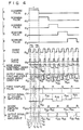
- Fig. 4 shows the signal waveforms used in explaining the mode of operation of the embodiment shown in Fig. 3 when a photoelectric conversion element array includes elements 1 1 to 1 s .
- the phase relations of pulses ⁇ IN , ⁇ R , ⁇ SP1 and ⁇ SP2 corresponding to the scanning pulses ⁇ P1 to ⁇ s are the same.
- the mode of operation of the embodiment shown in Fig. 3 may therefore be described with reference to only a scanning pulse ⁇ 1 .
- the rising time of that scanning pulse ⁇ 1 is designated by t1
- its falling time is designated by t9
- An inhibit pulse ⁇ IN corresponding to time t1 falls at time t2, and an inhibit pulse ⁇ IN corresponding to time t9 rises at time t8.
- An inhibit pulse ⁇ IN corresponding to a time point substantially intermediate during the time period T rises at time t4 and falls at time t6. Therefore, the analog switch 3 1 is turned on for a first time period TA between the times t2 and t4 and a second time period TB between the times t6 and t8 (Fig. 4F).
- a first clear pulse (P R supplied to the analog switch 3 1 rises at time t1 and falls at time t2.
- a second clear pulse (OR rises at time t5 and falls at time t6.
- the first amplifier 6 produces a noise signal component e N1 from the time t2 to t5 and from the time t6 to t9 (Fig. 4H).
- the first amplifier 6 produces a first signal e S1 from time t2 to t5, and a second signal e N1 from time t6 to t9.
- the second signal e N1 includes only the noise signal component e N1 .
- the first signal e 1s includes an image signal component corresponding to the amount of charge stored in the photodiode 1 1 , and a noise signal component e N1 , as well.
- the second signal e N1 includes only the noise signal component e N1 , since the charge stored in the photodiode 1 1 is practically discharged in time interval TA.
- the pulse width of the sampling pulse ⁇ PSP1 is from time t3 to t4 (Fig. 4J). Therefore, the first signal e S1 is sampled and is stored on the capacitor 12 while the analog switch 16 is turned on from time t3 to t4.
- the output level of the second amplifier 15 is given as e S1 , as shown in Fig. 4K. More specifically, the output level from the second amplifier 15 is kept at the level of the first signal e S1 , until the rising time of the sampling pulse ⁇ SP1 corresponding to the scanning pulse ⁇ 2 (Fig. 4K).
- the differential amplifier 13 produces a signal e S1 -e N1 , i.e., an image signal from the photodiode 1 1 , which signal does not contain the noise signal component e N1 .
- This image signal is charged on the capacitor 19, through the analog switch 18, by a sampling pulse ⁇ SP2 (Fig. 2L) having a pulse width of from T7 to T8.
- the image signal e S1 -e N1 is produced as a video signal e S1 -e N1 , from the third amplifier 14 (Fig. 4M).
- video signals e S2 -e N2 ; e S3 -e N3 ; e S4 -e N4 ; e S5 -e N5 which represent the image signals from the photodiodes 3 2 to 3 5 can also be obtained corresponding to the scanning pulses ⁇ 2 to ⁇ 5 .
- the amplitudes of the resultant video signals become uniform, as shown in Fig. 4M.
Landscapes
- Engineering & Computer Science (AREA)
- Multimedia (AREA)
- Signal Processing (AREA)
- Facsimile Heads (AREA)
- Transforming Light Signals Into Electric Signals (AREA)
- Solid State Image Pick-Up Elements (AREA)
Claims (6)
dadurch gekennzeichnet, daß der photoelektrische Umsetzungsapparat ferner aufweist:
Applications Claiming Priority (2)
| Application Number | Priority Date | Filing Date | Title |
|---|---|---|---|
| JP195572/82 | 1982-11-08 | ||
| JP57195572A JPS5986379A (ja) | 1982-11-08 | 1982-11-08 | 光電変換装置 |
Publications (3)
| Publication Number | Publication Date |
|---|---|
| EP0108308A2 EP0108308A2 (de) | 1984-05-16 |
| EP0108308A3 EP0108308A3 (en) | 1987-03-25 |
| EP0108308B1 true EP0108308B1 (de) | 1990-01-03 |
Family
ID=16343351
Family Applications (1)
| Application Number | Title | Priority Date | Filing Date |
|---|---|---|---|
| EP83110484A Expired EP0108308B1 (de) | 1982-11-08 | 1983-10-20 | Photo-elektrischer Umsetzungsapparat |
Country Status (5)
| Country | Link |
|---|---|
| US (1) | US4600843A (de) |
| EP (1) | EP0108308B1 (de) |
| JP (1) | JPS5986379A (de) |
| KR (1) | KR880000666B1 (de) |
| DE (1) | DE3381074D1 (de) |
Families Citing this family (21)
| Publication number | Priority date | Publication date | Assignee | Title |
|---|---|---|---|---|
| DE3525395A1 (de) * | 1984-07-17 | 1986-01-30 | Canon K.K., Tokio/Tokyo | Bildlesevorrichtung |
| JPH0624235B2 (ja) * | 1984-08-16 | 1994-03-30 | セイコーエプソン株式会社 | イメ−ジセンサチツプ |
| JPS6262671A (ja) * | 1985-09-12 | 1987-03-19 | Canon Inc | 固体撮像素子の信号処理回路 |
| JPH084127B2 (ja) * | 1986-09-30 | 1996-01-17 | キヤノン株式会社 | 光電変換装置 |
| US5737016A (en) * | 1985-11-15 | 1998-04-07 | Canon Kabushiki Kaisha | Solid state image pickup apparatus for reducing noise |
| US4914519A (en) * | 1986-09-19 | 1990-04-03 | Canon Kabushiki Kaisha | Apparatus for eliminating noise in a solid-state image pickup device |
| US5771070A (en) * | 1985-11-15 | 1998-06-23 | Canon Kabushiki Kaisha | Solid state image pickup apparatus removing noise from the photoelectric converted signal |
| JPS62122461A (ja) * | 1985-11-22 | 1987-06-03 | Fuji Photo Film Co Ltd | ラインセンサの読取回路 |
| GB8606200D0 (en) * | 1986-03-13 | 1986-04-16 | Crosfield Electronics Ltd | Operating radiation sensors |
| US4858022A (en) * | 1986-09-05 | 1989-08-15 | Kabushiki Kaisha Toshiba | Contact-type linear image sensor |
| GB2222249B (en) * | 1988-08-24 | 1992-07-08 | Rosemount Ltd | Optical sensor |
| US4902886A (en) * | 1989-01-23 | 1990-02-20 | Hewlett-Packard Company | Noise reduction for photodiode arrays |
| US5010408A (en) * | 1989-09-25 | 1991-04-23 | Eastman Kodak Company | Doubly correlated sample and hold circuit |
| US4987321A (en) * | 1989-09-25 | 1991-01-22 | Eastman Kodak Company | Processing circuit for image sensor |
| JP3431995B2 (ja) * | 1993-06-03 | 2003-07-28 | キヤノン株式会社 | 撮像装置 |
| US5475427A (en) * | 1994-05-25 | 1995-12-12 | Eastman Kodak Company | Video signal noise suppression circuit |
| JP3774499B2 (ja) | 1996-01-24 | 2006-05-17 | キヤノン株式会社 | 光電変換装置 |
| US9871588B2 (en) | 2015-12-30 | 2018-01-16 | Surefire Llc | Systems and methods for tiling optically narrowcast signals |
| US9853740B1 (en) * | 2017-06-06 | 2017-12-26 | Surefire Llc | Adaptive communications focal plane array |
| US10236986B1 (en) | 2018-01-05 | 2019-03-19 | Aron Surefire, Llc | Systems and methods for tiling free space optical transmissions |
| US10250948B1 (en) | 2018-01-05 | 2019-04-02 | Aron Surefire, Llc | Social media with optical narrowcasting |
Family Cites Families (7)
| Publication number | Priority date | Publication date | Assignee | Title |
|---|---|---|---|---|
| JPS5619786B2 (de) * | 1975-02-20 | 1981-05-09 | ||
| FR2356328A1 (fr) * | 1976-06-24 | 1978-01-20 | Ibm France | Dispositif d'elimination du bruit dans les reseaux photosensibles a auto-balayage |
| JPS5822900B2 (ja) * | 1978-09-25 | 1983-05-12 | 株式会社日立製作所 | 固体撮像装置 |
| US4287441A (en) * | 1979-03-30 | 1981-09-01 | The United States Of America As Represented By The Secretary Of The Army | Correlated double sampling CCD video preprocessor-amplifier |
| JPS56116374A (en) * | 1980-02-20 | 1981-09-12 | Sony Corp | Charge detection circuit |
| US4390894A (en) * | 1980-08-20 | 1983-06-28 | U.S. Philips Corporation | Noise suppression circuit for a video signal |
| JPS5884568A (ja) * | 1981-11-13 | 1983-05-20 | Fuji Xerox Co Ltd | 原稿読取装置 |
-
1982
- 1982-11-08 JP JP57195572A patent/JPS5986379A/ja active Pending
-
1983
- 1983-10-20 DE DE8383110484T patent/DE3381074D1/de not_active Expired - Lifetime
- 1983-10-20 EP EP83110484A patent/EP0108308B1/de not_active Expired
- 1983-10-27 US US06/546,191 patent/US4600843A/en not_active Expired - Fee Related
- 1983-11-08 KR KR8305282A patent/KR880000666B1/ko not_active Expired
Also Published As
| Publication number | Publication date |
|---|---|
| EP0108308A3 (en) | 1987-03-25 |
| JPS5986379A (ja) | 1984-05-18 |
| US4600843A (en) | 1986-07-15 |
| KR880000666B1 (en) | 1988-04-20 |
| DE3381074D1 (de) | 1990-02-08 |
| EP0108308A2 (de) | 1984-05-16 |
Similar Documents
| Publication | Publication Date | Title |
|---|---|---|
| US4600843A (en) | Photoelectric conversion apparatus | |
| US4523229A (en) | Shading correction device | |
| US5296696A (en) | Solid state image pickup apparatus and driving method | |
| US4283742A (en) | Solid-state imaging apparatus with fixed pattern noise reduction | |
| JPS6314553B2 (de) | ||
| US4472744A (en) | Photoelectric converter apparatus | |
| GB2137840A (en) | Automatic focus detecting | |
| US4413283A (en) | Solid-state imaging device | |
| US7102115B2 (en) | Photoelectric converter and a method of driving the same | |
| US4609825A (en) | Device for modulating the sensitivity of a line-transfer photosensitive device | |
| US4914319A (en) | Signal reading circuit | |
| US20020166949A1 (en) | Photoelectic converter | |
| JP3571934B2 (ja) | イメージセンサー | |
| US4857996A (en) | Image pickup device with reduced fixed pattern noise | |
| RU2145154C1 (ru) | Устройство однократного формирования сигнала изображения | |
| JP2671307B2 (ja) | 固体撮像装置 | |
| US5731833A (en) | Solid-state image pick-up device with reference level clamping and image pick-up apparatus using the same | |
| JP3332375B2 (ja) | 撮像装置 | |
| JPH11220566A (ja) | イメージセンサー | |
| JP3172359B2 (ja) | 撮像装置 | |
| JP2817218B2 (ja) | 固体撮像装置 | |
| SU1352435A1 (ru) | Устройство регистрации | |
| JP3603454B2 (ja) | 撮像装置 | |
| JP3093645B2 (ja) | 電荷蓄積型受光部を有した撮像装置 | |
| JPH06233054A (ja) | Ccdラインセンサ駆動装置 |
Legal Events
| Date | Code | Title | Description |
|---|---|---|---|
| PUAI | Public reference made under article 153(3) epc to a published international application that has entered the european phase |
Free format text: ORIGINAL CODE: 0009012 |
|
| 17P | Request for examination filed |
Effective date: 19831117 |
|
| AK | Designated contracting states |
Designated state(s): DE FR GB IT NL |
|
| RAP1 | Party data changed (applicant data changed or rights of an application transferred) |
Owner name: KABUSHIKI KAISHA TOSHIBA |
|
| PUAL | Search report despatched |
Free format text: ORIGINAL CODE: 0009013 |
|
| AK | Designated contracting states |
Kind code of ref document: A3 Designated state(s): DE FR GB IT NL |
|
| 17Q | First examination report despatched |
Effective date: 19890222 |
|
| GRAA | (expected) grant |
Free format text: ORIGINAL CODE: 0009210 |
|
| AK | Designated contracting states |
Kind code of ref document: B1 Designated state(s): DE FR GB IT NL |
|
| ITF | It: translation for a ep patent filed | ||
| REF | Corresponds to: |
Ref document number: 3381074 Country of ref document: DE Date of ref document: 19900208 |
|
| ET | Fr: translation filed | ||
| PLBE | No opposition filed within time limit |
Free format text: ORIGINAL CODE: 0009261 |
|
| STAA | Information on the status of an ep patent application or granted ep patent |
Free format text: STATUS: NO OPPOSITION FILED WITHIN TIME LIMIT |
|
| 26N | No opposition filed | ||
| ITTA | It: last paid annual fee | ||
| PGFP | Annual fee paid to national office [announced via postgrant information from national office to epo] |
Ref country code: GB Payment date: 19941011 Year of fee payment: 12 Ref country code: FR Payment date: 19941011 Year of fee payment: 12 |
|
| PGFP | Annual fee paid to national office [announced via postgrant information from national office to epo] |
Ref country code: DE Payment date: 19941021 Year of fee payment: 12 |
|
| PGFP | Annual fee paid to national office [announced via postgrant information from national office to epo] |
Ref country code: NL Payment date: 19941031 Year of fee payment: 12 |
|
| PG25 | Lapsed in a contracting state [announced via postgrant information from national office to epo] |
Ref country code: GB Effective date: 19951020 |
|
| PG25 | Lapsed in a contracting state [announced via postgrant information from national office to epo] |
Ref country code: NL Effective date: 19960501 |
|
| GBPC | Gb: european patent ceased through non-payment of renewal fee |
Effective date: 19951020 |
|
| PG25 | Lapsed in a contracting state [announced via postgrant information from national office to epo] |
Ref country code: FR Effective date: 19960628 |
|
| PG25 | Lapsed in a contracting state [announced via postgrant information from national office to epo] |
Ref country code: DE Effective date: 19960702 |
|
| NLV4 | Nl: lapsed or anulled due to non-payment of the annual fee |
Effective date: 19960501 |
|
| REG | Reference to a national code |
Ref country code: FR Ref legal event code: ST |