EP0109139A2 - Halbleiterspeicher mit einer ladungsgepumpten Schaltung - Google Patents
Halbleiterspeicher mit einer ladungsgepumpten Schaltung Download PDFInfo
- Publication number
- EP0109139A2 EP0109139A2 EP83303858A EP83303858A EP0109139A2 EP 0109139 A2 EP0109139 A2 EP 0109139A2 EP 83303858 A EP83303858 A EP 83303858A EP 83303858 A EP83303858 A EP 83303858A EP 0109139 A2 EP0109139 A2 EP 0109139A2
- Authority
- EP
- European Patent Office
- Prior art keywords
- output terminal
- transistor
- mos transistor
- terminal voltage
- circuit
- Prior art date
- Legal status (The legal status is an assumption and is not a legal conclusion. Google has not performed a legal analysis and makes no representation as to the accuracy of the status listed.)
- Granted
Links
Images

Classifications
-
- G—PHYSICS
- G11—INFORMATION STORAGE
- G11C—STATIC STORES
- G11C11/00—Digital stores characterised by the use of particular electric or magnetic storage elements; Storage elements therefor
- G11C11/21—Digital stores characterised by the use of particular electric or magnetic storage elements; Storage elements therefor using electric elements
- G11C11/34—Digital stores characterised by the use of particular electric or magnetic storage elements; Storage elements therefor using electric elements using semiconductor devices
- G11C11/40—Digital stores characterised by the use of particular electric or magnetic storage elements; Storage elements therefor using electric elements using semiconductor devices using transistors
- G11C11/401—Digital stores characterised by the use of particular electric or magnetic storage elements; Storage elements therefor using electric elements using semiconductor devices using transistors forming cells needing refreshing or charge regeneration, i.e. dynamic cells
- G11C11/4063—Auxiliary circuits, e.g. for addressing, decoding, driving, writing, sensing or timing
- G11C11/407—Auxiliary circuits, e.g. for addressing, decoding, driving, writing, sensing or timing for memory cells of the field-effect type
- G11C11/408—Address circuits
- G11C11/4085—Word line control circuits, e.g. word line drivers, - boosters, - pull-up, - pull-down, - precharge
-
- G—PHYSICS
- G11—INFORMATION STORAGE
- G11C—STATIC STORES
- G11C11/00—Digital stores characterised by the use of particular electric or magnetic storage elements; Storage elements therefor
- G11C11/21—Digital stores characterised by the use of particular electric or magnetic storage elements; Storage elements therefor using electric elements
- G11C11/34—Digital stores characterised by the use of particular electric or magnetic storage elements; Storage elements therefor using electric elements using semiconductor devices
- G11C11/40—Digital stores characterised by the use of particular electric or magnetic storage elements; Storage elements therefor using electric elements using semiconductor devices using transistors
- G11C11/401—Digital stores characterised by the use of particular electric or magnetic storage elements; Storage elements therefor using electric elements using semiconductor devices using transistors forming cells needing refreshing or charge regeneration, i.e. dynamic cells
- G11C11/4063—Auxiliary circuits, e.g. for addressing, decoding, driving, writing, sensing or timing
- G11C11/407—Auxiliary circuits, e.g. for addressing, decoding, driving, writing, sensing or timing for memory cells of the field-effect type
- G11C11/409—Read-write [R-W] circuits
- G11C11/4094—Bit-line management or control circuits
-
- G—PHYSICS
- G11—INFORMATION STORAGE
- G11C—STATIC STORES
- G11C5/00—Details of stores covered by group G11C11/00
- G11C5/14—Power supply arrangements, e.g. power down, chip selection or deselection, layout of wirings or power grids, or multiple supply levels
- G11C5/145—Applications of charge pumps; Boosted voltage circuits; Clamp circuits therefor
Definitions
- the present invention relates to a semiconductor device and more particularly to an output circuit thereof.
- various clocks are used to actuate the respective parts of the memory in predetermined relationships of timing.
- the power source voltage is reduced from 12 V to a level of 5 V and the element size is reduced. Accordingly, the accumulated charge in each memory cell is very small.
- the clock amplitudes are increased to a value greater than the power source voltage.
- an output-level guaranteeing circuit utilizing a charge-pumping circuit involves a certain problem at the time of application of power.
- a clock pulse of the charge-pumping circuit is usually led out of a substrate bias-voltage generating circuit, and this substrate bias-voltage generating circuit starts operation substantially simultaneous with the application of power source voltage so that the clock pulse is simultaneously produced.
- clock pulses for actuating a buffer circuit connected before the output circuit are led out of predetermined stages of the various clock pulse generators connected in multiple stages. Therefore, in these clock pulses, predetermined logic levels are hardly attained at the time of application of the power source voltage.
- these clock pulses for actuating a buffer circuit are all at a low level, the output is in the floating state.
- An embodiment of the present invention can provide a semiconductor device provided with a buffer, which device comprises a first transistor for pulling up the output terminal voltage, a second transistor for pulling down the output terminal voltage, and a charge-pumping circuit for maintaining the output terminal voltage at a level higher than the power source voltage by charge pumping when the output terminal voltage is at a high level, said semiconductor device being characterized in that it further comprises a circuit for pulling down the output terminal voltage during the period from the point of application of power to the point of initiation of supply of an input signal to the buffer.
- Figure 1 shows a circuit for generating a second clock pulse ⁇ 2 which rises on the receipt of a first clock pulse ⁇ 1 and drops on the receipt of a reset clock pulse ⁇ R .
- Q1 through Q13 represents metal--oxide semiconductor (MOS) transistors
- Cl and C2 represent capacitors
- Vcc and Vss represent H (high) and L (low) levels of a 5V power source
- OUT represents an output.
- the transistors Q2 and Q3 are turned on, the transistor Q4 is turned off, the transistors Q9 and Qll are turned on, the transistor Q7 is turned on, the transistors Q8 and Q10 are turned off, and the voltage ⁇ 2 of the output is maintained at a low level L.
- the gate of the transistor Q6 is charged at a high level H through the gate Q5.
- the transistor Ql is turned on, the transistors Q2, Q3, and Q7 are turned off, the transistor Q4 is turned on, the transistors Q8 and Q10 are turned on, the transistors Q9 and Qll are turned off, and the output OUT ( ⁇ 2 ) as shown in Fig. 2A is maintained at a high level H.
- Fig. 2A the relationships among the clock pulses ⁇ 1 , and ⁇ R , the potentials at nodes N 2 and N 3 , and the output ⁇ 2 are illustrated.
- the potential level at the node N 2 is placed at a level higher than the electric source voltage Vcc so that the output level of the output O 2 is obtained.
- Vcc electric source voltage
- the clock pulse ⁇ 3 is generated for actuating the charge-pumping circuit including transistors Q12 and Q13 and the capacitor C2. More specifically, when the clock pulse ⁇ 3 is at a low level L, the capacitor C2 is charged through the Vcc, Q13, and C2, and when the clock pulse ⁇ 3 is at a high level H, the charge of this capacitor C2 charges the output OUT through the transistor Q12. The frequency of the clock pulse ⁇ 3 is high, and, therefore, the above-mentioned pumping operation is repeated at a high speed.
- the clock pulse ⁇ R is put in the circuit, as was pointed out hereinbefore, the transistor Qll is turned on, and, hence, the level of the output OUT is reduced to a low level L.
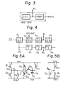
- the operation state is as follows. Namely, the clock pulse ⁇ 3 is led out of a substrate bias-voltage generating circuit V BB GEN.
- the circuit V BB GEN comprises an oscillator OSC and a pumping circuit PUMP. Substantially simultaneous with application of the power source voltage Vcc, the circuit V BB GEN starts operation, and hence, the clock pulse ⁇ 3 is simultaneously produced.
- the clock pulses ⁇ 1 and ⁇ R are led out of predetermined stages of various clock generators G1, G2, .... and Ri, R2, ....
- CS represents a chip-select bar signal
- ADDBUF represents an address buffer
- WD represents a word decoder
- S/A represents a sense amplifier
- RST represents a reset.
- the transistor Q13 If the clock pulse ⁇ 3 is generated simultaneous with the rising of the Vcc, the transistor Q13 is turned on, though insufficiently, and the capacitor C2 is charged by the Vcc when th clock pulse ⁇ 3 is at a low level and the capacitor C2 charges the output OUT through the transistors Q12 when the clock pulse ⁇ 3 is at a high level H.
- the capacitor C2 repeats this operation; and the voltage at the node N1 rises as indicated in the portion Tl of Fig. 2B. Also, the voltage of the output OUT is caused to rise.
- the first and second transistors for receiving the clock pulse ⁇ 2 and other clock pulses are connected in series between the terminals of the power source and short circuiting of the power source is prevented since one of the transistors is turned off by supply of the other clock pulse to the other transistor when the clock signal is supplied to one transistor, if the clock pulse ⁇ 2 is supplied for the above-mentioned reason before the other clock pulses are supplied, both the first and second transistors are turned on and short circuiting of the power source occurs.
- FIG. 5A shows an embodiment of the present invention.
- Q10 and Q11 represents output stage transistors of the buffer or clock generator shown in Fig. 1
- OUT represents the output of the buffer or clock generator
- Q12, Q13, and C2 form a charge- rcuit for the output OUT.
- an MOS transistor is disposed to pull down the output terminal voltage to a low voltage line Vss of the power source.
- the transistor Q15 and Q16 are MOS transistors for controlling the gate voltage of the transistor Q14.
- the transistor Q15 is a depletion-type transistor, but an enhancement-type transistor as shown in Fig. 5B may be used.
- the gate of this transistor is connected to the high voltage side.
- the transistor Q16 is an enhancement-type transistor, and a clock pulse ⁇ 4 is received by the gate of this transistor. Any clock pulse may be used as the clock pulse ⁇ 4 if it is of the same phase as that of the clock pulse ⁇ 2 .
- a clock pulse ⁇ 1 ' to be supplied in the transistor Q10 or the output clock pulse ⁇ 2 per se may be used.
- the mutual conductance of the transistor Q14 is made smaller than that of the transistor Q10. Namely, the resistance of Q14 is made higher than that of Q10. Even if the resistance of Q14 is high , the rising of the output OUT due to incomplete pumping at the time of the rising of the power source voltage Vcc can be controlled sufficiently.
- the clock pulse ⁇ 1 ' is then supplied to turn on the transistor Q10 and turn off the transistor Qll, the output terminal voltage OUT is pulled up to the power source voltage Vcc by the transistor Q10 and the output voltage OUT rises. Accordingly, the transistor Q16 is turned on and the transistor Q14 is turned off, and the output terminal voltage is no longer pulled down. In short, a kind of positive feedback is applied to the output OUT.
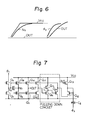
- Figure 7 shows another embodiment of the present invention.
- the same elements as those in Fig. 5A are represented by the same symbols as those in Fig. 5A.
- the circuit for pulling down the output terminal voltage is indirectly connected to the output of the buffer circuit, that is, the gate of the transistor Q16 is connected via transistors Q17 and Q18 to the output of the buffer circuit, and the connecting point between the drain of the transistor Q14 and the source of the transistor Q14 is connected to the node N 2 .
- the node N 2 to be pumped is pulled down so that the same effect as that produced by the circuit shown in Fig. 5A can be obtained.
Landscapes
- Engineering & Computer Science (AREA)
- Microelectronics & Electronic Packaging (AREA)
- Computer Hardware Design (AREA)
- Power Engineering (AREA)
- Dc-Dc Converters (AREA)
- Dram (AREA)
- Electronic Switches (AREA)
- Semiconductor Memories (AREA)
Applications Claiming Priority (2)
| Application Number | Priority Date | Filing Date | Title |
|---|---|---|---|
| JP114244/82 | 1982-07-01 | ||
| JP57114244A JPS595488A (ja) | 1982-07-01 | 1982-07-01 | 半導体装置 |
Publications (3)
| Publication Number | Publication Date |
|---|---|
| EP0109139A2 true EP0109139A2 (de) | 1984-05-23 |
| EP0109139A3 EP0109139A3 (en) | 1986-09-03 |
| EP0109139B1 EP0109139B1 (de) | 1989-09-13 |
Family
ID=14632889
Family Applications (1)
| Application Number | Title | Priority Date | Filing Date |
|---|---|---|---|
| EP83303858A Expired EP0109139B1 (de) | 1982-07-01 | 1983-07-01 | Halbleiterspeicher mit einer ladungsgepumpten Schaltung |
Country Status (5)
| Country | Link |
|---|---|
| US (1) | US4570088A (de) |
| EP (1) | EP0109139B1 (de) |
| JP (1) | JPS595488A (de) |
| DE (1) | DE3380577D1 (de) |
| IE (1) | IE55208B1 (de) |
Cited By (1)
| Publication number | Priority date | Publication date | Assignee | Title |
|---|---|---|---|---|
| EP0552404A1 (de) * | 1992-07-23 | 1993-07-28 | Siemens Aktiengesellschaft | Schaltungsanordnung zur Begrenzung der Ausgangsspannung einer Spannungserhöhungsschaltung |
Families Citing this family (8)
| Publication number | Priority date | Publication date | Assignee | Title |
|---|---|---|---|---|
| JPH077599B2 (ja) * | 1984-05-25 | 1995-01-30 | 株式会社日立製作所 | 半導体集積回路装置 |
| JP2548908B2 (ja) * | 1985-04-13 | 1996-10-30 | 富士通株式会社 | 昇圧回路 |
| US4701633A (en) * | 1985-04-30 | 1987-10-20 | Texas Instruments Incorporated | Low power clock generator |
| JPS62159917A (ja) * | 1986-01-08 | 1987-07-15 | Toshiba Corp | 集積回路におけるインバ−タ回路 |
| KR970000560B1 (ko) * | 1986-10-01 | 1997-01-13 | 아오이 죠이치 | 반도체집적회로 |
| JPH0789434B2 (ja) * | 1986-11-12 | 1995-09-27 | 日本電気株式会社 | ダイナミツク型記憶装置 |
| KR100307514B1 (ko) * | 1994-07-30 | 2001-12-01 | 김영환 | 차지펌프회로 |
| KR19990057914A (ko) * | 1997-12-30 | 1999-07-15 | 김영환 | 지연고정루프의 차지펌핑회로 |
Family Cites Families (10)
| Publication number | Priority date | Publication date | Assignee | Title |
|---|---|---|---|---|
| DE2433328A1 (de) * | 1974-07-11 | 1976-01-29 | Philips Patentverwaltung | Integrierte schaltungsanordnung |
| US4061933A (en) * | 1975-12-29 | 1977-12-06 | Mostek Corporation | Clock generator and delay stage |
| US4097772A (en) * | 1977-06-06 | 1978-06-27 | Motorola, Inc. | MOS switch with hysteresis |
| US4291242A (en) * | 1979-05-21 | 1981-09-22 | Motorola, Inc. | Driver circuit for use in an output buffer |
| US4296340A (en) * | 1979-08-27 | 1981-10-20 | Intel Corporation | Initializing circuit for MOS integrated circuits |
| JPS5693422A (en) * | 1979-12-05 | 1981-07-29 | Fujitsu Ltd | Level-up circuit |
| JPS56117390A (en) * | 1980-02-16 | 1981-09-14 | Fujitsu Ltd | Semiconductor memory device |
| WO1982000930A1 (en) * | 1980-09-10 | 1982-03-18 | Plachno R | Delay stage for a clock generator |
| JPS5788594A (en) * | 1980-11-19 | 1982-06-02 | Fujitsu Ltd | Semiconductor circuit |
| JPS583325A (ja) * | 1981-06-29 | 1983-01-10 | Fujitsu Ltd | インバ−タ回路 |
-
1982
- 1982-07-01 JP JP57114244A patent/JPS595488A/ja active Granted
-
1983
- 1983-07-01 EP EP83303858A patent/EP0109139B1/de not_active Expired
- 1983-07-01 DE DE8383303858T patent/DE3380577D1/de not_active Expired
- 1983-07-01 US US06/510,183 patent/US4570088A/en not_active Expired - Fee Related
- 1983-07-01 IE IE1555/83A patent/IE55208B1/en not_active IP Right Cessation
Cited By (1)
| Publication number | Priority date | Publication date | Assignee | Title |
|---|---|---|---|---|
| EP0552404A1 (de) * | 1992-07-23 | 1993-07-28 | Siemens Aktiengesellschaft | Schaltungsanordnung zur Begrenzung der Ausgangsspannung einer Spannungserhöhungsschaltung |
Also Published As
| Publication number | Publication date |
|---|---|
| DE3380577D1 (en) | 1989-10-19 |
| JPS595488A (ja) | 1984-01-12 |
| EP0109139B1 (de) | 1989-09-13 |
| EP0109139A3 (en) | 1986-09-03 |
| JPH0154799B2 (de) | 1989-11-21 |
| IE55208B1 (en) | 1990-07-04 |
| IE831555L (en) | 1984-01-01 |
| US4570088A (en) | 1986-02-11 |
Similar Documents
| Publication | Publication Date | Title |
|---|---|---|
| US4115710A (en) | Substrate bias for MOS integrated circuit | |
| US5757714A (en) | Semiconductor memory device with on-chip boosted power supply voltage generator | |
| US5532640A (en) | Voltage generator circuit generating stable negative potential | |
| US6137343A (en) | Semiconductor memory device equipped with voltage generator circuit | |
| US4649289A (en) | Circuit for maintaining the potential of a node of a MOS dynamic circuit | |
| EP0109139B1 (de) | Halbleiterspeicher mit einer ladungsgepumpten Schaltung | |
| US6225854B1 (en) | Voltage boosting circuit having cross-coupled precharge circuits | |
| EP0052504B1 (de) | Halbleiterpufferverstärkerschaltung | |
| EP0032017A1 (de) | Bootstrapschaltung | |
| US5124574A (en) | Semiconductor device for generating a voltage higher than power source potential or lower than grounding potential | |
| JP2632112B2 (ja) | 電圧発生回路 | |
| US5436586A (en) | Semiconductor integrated circuit apparatus including supply voltage conversion circuit | |
| US5786719A (en) | Mode setting circuit and mode setting apparatus used to select a particular semiconductor function | |
| KR100586750B1 (ko) | 전위 부스트 회로 | |
| US4716303A (en) | MOS IC pull-up circuit | |
| KR100347355B1 (ko) | 승압회로및그구동방법 | |
| KR0149224B1 (ko) | 반도체 집적장치의 내부전압 승압회로 | |
| US5175448A (en) | Booster circuit | |
| EP0148364B1 (de) | Zeitsignalgenerator | |
| US4833343A (en) | Clock generator having complementary transistors | |
| KR100548557B1 (ko) | 반도체 장치의 내부 전원발생장치 | |
| JPH1069796A (ja) | 高速試験機能付半導体集積回路 | |
| KR0172242B1 (ko) | 고전압 발생회로 | |
| KR100432985B1 (ko) | 상승된출력전압을발생시키기위한회로 | |
| KR0132023B1 (ko) | 다단 펌프회로를 이용한 전압 발생기 |
Legal Events
| Date | Code | Title | Description |
|---|---|---|---|
| PUAI | Public reference made under article 153(3) epc to a published international application that has entered the european phase |
Free format text: ORIGINAL CODE: 0009012 |
|
| AK | Designated contracting states |
Designated state(s): DE FR GB |
|
| PUAL | Search report despatched |
Free format text: ORIGINAL CODE: 0009013 |
|
| AK | Designated contracting states |
Kind code of ref document: A3 Designated state(s): DE FR GB |
|
| 17P | Request for examination filed |
Effective date: 19861003 |
|
| 17Q | First examination report despatched |
Effective date: 19871112 |
|
| GRAA | (expected) grant |
Free format text: ORIGINAL CODE: 0009210 |
|
| AK | Designated contracting states |
Kind code of ref document: B1 Designated state(s): DE FR GB |
|
| REF | Corresponds to: |
Ref document number: 3380577 Country of ref document: DE Date of ref document: 19891019 |
|
| ET | Fr: translation filed | ||
| PLBE | No opposition filed within time limit |
Free format text: ORIGINAL CODE: 0009261 |
|
| STAA | Information on the status of an ep patent application or granted ep patent |
Free format text: STATUS: NO OPPOSITION FILED WITHIN TIME LIMIT |
|
| 26N | No opposition filed | ||
| PGFP | Annual fee paid to national office [announced via postgrant information from national office to epo] |
Ref country code: GB Payment date: 19920428 Year of fee payment: 10 |
|
| PGFP | Annual fee paid to national office [announced via postgrant information from national office to epo] |
Ref country code: FR Payment date: 19920730 Year of fee payment: 10 |
|
| PGFP | Annual fee paid to national office [announced via postgrant information from national office to epo] |
Ref country code: DE Payment date: 19920922 Year of fee payment: 10 |
|
| PG25 | Lapsed in a contracting state [announced via postgrant information from national office to epo] |
Ref country code: GB Effective date: 19930701 |
|
| GBPC | Gb: european patent ceased through non-payment of renewal fee |
Effective date: 19930701 |
|
| PG25 | Lapsed in a contracting state [announced via postgrant information from national office to epo] |
Ref country code: FR Effective date: 19940331 |
|
| PG25 | Lapsed in a contracting state [announced via postgrant information from national office to epo] |
Ref country code: DE Effective date: 19940401 |
|
| REG | Reference to a national code |
Ref country code: FR Ref legal event code: ST |