EP0109490A2 - Vorrichtung zum Unterscheiden papierähnlichen Materials - Google Patents
Vorrichtung zum Unterscheiden papierähnlichen Materials Download PDFInfo
- Publication number
- EP0109490A2 EP0109490A2 EP83108424A EP83108424A EP0109490A2 EP 0109490 A2 EP0109490 A2 EP 0109490A2 EP 83108424 A EP83108424 A EP 83108424A EP 83108424 A EP83108424 A EP 83108424A EP 0109490 A2 EP0109490 A2 EP 0109490A2
- Authority
- EP
- European Patent Office
- Prior art keywords
- value
- paper
- pattern data
- presettable
- detection area
- Prior art date
- Legal status (The legal status is an assumption and is not a legal conclusion. Google has not performed a legal analysis and makes no representation as to the accuracy of the status listed.)
- Granted
Links
- 239000000463 material Substances 0.000 title claims description 28
- 238000001514 detection method Methods 0.000 claims abstract description 25
- 230000007547 defect Effects 0.000 claims abstract description 18
- 230000003287 optical effect Effects 0.000 claims abstract description 15
- 238000005070 sampling Methods 0.000 claims abstract description 14
- 238000011109 contamination Methods 0.000 description 3
- 230000002411 adverse Effects 0.000 description 2
- 238000006243 chemical reaction Methods 0.000 description 2
- 238000010586 diagram Methods 0.000 description 2
- 238000000151 deposition Methods 0.000 description 1
- 238000005562 fading Methods 0.000 description 1
- 230000006870 function Effects 0.000 description 1
- 238000004519 manufacturing process Methods 0.000 description 1
- 238000012986 modification Methods 0.000 description 1
- 230000004048 modification Effects 0.000 description 1
- 238000002360 preparation method Methods 0.000 description 1
- 239000002689 soil Substances 0.000 description 1
Images


Classifications
-
- G—PHYSICS
- G07—CHECKING-DEVICES
- G07D—HANDLING OF COINS OR VALUABLE PAPERS, e.g. TESTING, SORTING BY DENOMINATIONS, COUNTING, DISPENSING, CHANGING OR DEPOSITING
- G07D7/00—Testing specially adapted to determine the identity or genuineness of valuable papers or for segregating those which are unacceptable, e.g. banknotes that are alien to a currency
- G07D7/06—Testing specially adapted to determine the identity or genuineness of valuable papers or for segregating those which are unacceptable, e.g. banknotes that are alien to a currency using wave or particle radiation
- G07D7/12—Visible light, infrared or ultraviolet radiation
-
- G—PHYSICS
- G07—CHECKING-DEVICES
- G07D—HANDLING OF COINS OR VALUABLE PAPERS, e.g. TESTING, SORTING BY DENOMINATIONS, COUNTING, DISPENSING, CHANGING OR DEPOSITING
- G07D7/00—Testing specially adapted to determine the identity or genuineness of valuable papers or for segregating those which are unacceptable, e.g. banknotes that are alien to a currency
- G07D7/181—Testing mechanical properties or condition, e.g. wear or tear
- G07D7/187—Detecting defacement or contamination, e.g. dirt
-
- G—PHYSICS
- G07—CHECKING-DEVICES
- G07D—HANDLING OF COINS OR VALUABLE PAPERS, e.g. TESTING, SORTING BY DENOMINATIONS, COUNTING, DISPENSING, CHANGING OR DEPOSITING
- G07D7/00—Testing specially adapted to determine the identity or genuineness of valuable papers or for segregating those which are unacceptable, e.g. banknotes that are alien to a currency
- G07D7/20—Testing patterns thereon
- G07D7/202—Testing patterns thereon using pattern matching
Definitions
- This invention relates to an apparatus for discriminating a paper-like material.
- the paper-like material such as bank notes, securities and cheques
- problems such as fading of the original color of the material, contamination e.g., depositing of stains, and the printing ink drips from the material.
- an apparatus for discriminating a paper-like material comprising optical scanning means for projecting scanning light toward a detection area of the paper-like material which is being conveyed through the optical scanning means, photoelectric converting means for converting an optically scanned signal from the optical scanning means into an electric analog signal whose level is substantially in proportion to the level of the optically scanned signal, analog/digital converting means for converting the electric analog signal into a digital signal, timing control means for applying sampling pulses to the analog/digital converting means so as to produce a sampled digital value from the analog/digital converting means, storing means for storing at least a presettable value which is used to discriminate the paper-like material, and arithmetic operation means for performing the arithmetic operation by introducing the sampled digital value and the presettable value so as to discriminate defects in the detection area of the paper-like material.
- Fig. 1 shows a block diagram of an apparatus for discriminating a paper-like material according to a preferred embodiment._
- the apparatus shown in Fig. 1 is so designed as to discriminate a bank note 10.
- the note 10 is conveyed in the direction of an arrow 14 along,a convey path 12 at a given convey speed.
- a part of a front surface 16 of the note 10 is used as a detection area 30.
- This area is optically scanned in the conveying direction 14 so as to establish the entire detection area 30.
- a light source 18, coupled to a power source (not shown), and a light receiver 20 are positioned apart at a given distance from the detection area 30 of the front surface 16 of the note 10.
- This optical system is arranged in such a manner that light rays 21 radiated from the light source 18 are incident upon the detection area 30.
- the light receiver 20 receives the rays 23 reflected from the detection area 30.
- the optical signal of the light receiver 20 is supplied to a photoelectric converting circuit and converted into a corresponding electric signal.
- the electric output signal from the photoelectric converting circuit 24 is applied to an A/D converter 26.
- An output terminal of the A/D converter 26 is connected to an arithmetic logic unit 28 and also to a first memory section 32, second memory section 34, a third memory section 36, a counter 38 and a fourth memory section 40.
- a central control circuit 42 is provided in the apparatus.
- the output terminal of this circuit 42 is connected to an arithmetic logic unit 28, a first memory section 32, an second memory section 34, a third memory section 36, a counter 38, and a fourth memory section 40 so as to supply control signals to them.
- a timing control circuit 44 is provided to control the sampling timing of the A/D converter 26 and to apply its timing control information (sampling pulse signals) to the central control circuit 42.
- the function of the A/D converter 26, as is well known, is to convert analog (electric) signals obtained by optically-scanning the detection area 30 of the note 10 into digital signals.
- the digital signals are sampled by sampling pulse signals generated in the timing control circuit 44 and, then, the sampled digital signals are applied to a processing circuit.
- the first memory section 32 used as the main memory is functionally divided into a plurality of sub-regions for storing a standard pattern, an input pattern and data on the arithmetic operation.
- the second memory section 34 stores a level "E" (a first presettable value) which is used to produce a discrimination pattern, and the third memory section 36 stores a count "F" (a second presettable value).
- the arithmetic logic unit 28 (ALU) performs the arithmetic logic operation.
- the counter 38 is resettable and actuated by the ALU 28 and the third memory section 36.
- the central control circuit 42 controls the operations of the overall circuit.
- the fourth memory section 40 stores a third presettable value "K" which is used for discriminating that almost the entire note 10 is soiled.
- the first presettable level “E” must be set to a given value smaller than the maximum value of the output voltage signal derived from the photoelectric converting circuit, and the second presettable count “F” must be set to a given value or number is smaller than all sampling numbers of the A/D converter 26 with respect to one note 10.
- a print pattern of a standard bank note (not shown) which is clean is optically scanned by the light source 18, the light receiver 20 and the photoelectric converting circuit 24.
- the print pattern defined by the hatched area 30 is scanned by the above optical means along the conveying direction 14..(Therefore, the scanned entire area of the print pattern is identical with the detection area 30 in this specification.)
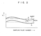
- the output analog signals shown in Fig. 2 by a curve "G" are supplied to the A/D converter 26.
- the timing control circuit 44 may produce e.g., "n" sampling pulses and apply them to the A/D converter 26 while a pattern of one note is being read out.
- the A/D converter 26 converts the analog signal output from the photoelectric converting circuit 24 into the corresponding digital signal during generation of the sampling pulse, and the thus converted digital signal is stored as a standard pattern data "PS" in the first memory section 32.
- the stored standard pattern data "Ps” is read from the first memory section 32 to ALU 28. From data "Ps” the average value (AVEST) is calculated (see Fig. 2). Thereafter the thus obtained average value (AVEST) is again stored in the first memory section 32.
- a note 10 to be discriminated for defects such as stains is optically scanned by the optical devices, which produce an output analog signal having a level "H" (see Fig. 2).
- the output analog signal is applied to the A/D converter 26.
- the level “H” of this output signal is lower than the level “G” of the output signal obtained by scanning the standard bank note. This means that the detection area 30 of the note 10 is soiled.
- the sampling pulse is applied to the A/D converter 26 from the timing control circuit 44.
- the resultant digital signal is stored as input pattern data "P I " in the first memory section 32.
- n sampling pulses for the note 10 are applied to the A/D converter 26. In other words, A/D conversion is carried out n times.
- the input pattern data "P I " is read from the first memory section 32 and its average value (AVEIN) is calculated by ALU 28.
- An average value difference (X) in a digital value between this average value (AVEIN) and the previously obtained one (AVEST) for the standard pattern is also calculated by ALU 28.
- the difference (X) of the average values is used to correct the input pattern data for every sampling pulse, i.e.,
- the input pattern data is shifted up if the difference (X) has a positie value, and is shifted down if the difference (X) has a negative value.
- the input pattern data "P I " is shifted up since the difference (X) has a positive value (see Fig. 2).
- the standard pattern data (P S ) is read from the first memory section 32 to ALU 28.
- the corrected input pattern (P I ') is subtracted from the standard pattern data (PS) for every sampling pulse so as to obtain a second difference (I). Then the second difference (I) is compared with the first presettable level (E) stored in the second memory section 34. Only when “I” is greater than or equal to "E”, the counter 38 counts up by "1". As was previously described, this counter is already initialized to "0". Such a comparison between the second difference (I) and the first presettable value (E) is repeated m times. This number, m, is equal to the number, n.
- the count (J) of the counter 38 is compared with the second presettable value (F) stored in the third memory section 36. If “J" is smaller than "F", the note 10 has no defect.
- the apparatus for discriminating defects in paper-like material, it can reliably discriminate defects of any kind in the print patterns without adverse influence from the print patterns themselves. Moreover, the apparatus is very useful because the user can freely preset the degree of the stain, i.e., the first presettable value "E", and also the area of the stain i.e., the second p resettable value "F".
- the third presettable value "K" stored in the fourth memory section may be omitted if the entire detection area of the paper-like material is not soiled.
- the difference "I” was calculated after the input pattern data "P I " had been corrected by the average value difference "X” and thereafter was compared with the first presettable value "E"
- the first presettable value "E” can be changed by the average value without average-correcting the input pattern data PI .
- the counter counted up from “0" in the embodiment.
- the second presettable value "F” may-be preset in the counter before the discriminating operation, and the counter may count down from the preset value, for example.
Landscapes
- Physics & Mathematics (AREA)
- General Physics & Mathematics (AREA)
- Health & Medical Sciences (AREA)
- General Health & Medical Sciences (AREA)
- Toxicology (AREA)
- Engineering & Computer Science (AREA)
- Computer Vision & Pattern Recognition (AREA)
- Inspection Of Paper Currency And Valuable Securities (AREA)
- Length Measuring Devices By Optical Means (AREA)
- Controlling Sheets Or Webs (AREA)
- Sorting Of Articles (AREA)
- Optical Radar Systems And Details Thereof (AREA)
Applications Claiming Priority (2)
| Application Number | Priority Date | Filing Date | Title |
|---|---|---|---|
| JP57166584A JPS5957108A (ja) | 1982-09-27 | 1982-09-27 | 紙葉類の損傷判定方式 |
| JP166584/82 | 1982-09-27 |
Publications (3)
| Publication Number | Publication Date |
|---|---|
| EP0109490A2 true EP0109490A2 (de) | 1984-05-30 |
| EP0109490A3 EP0109490A3 (en) | 1986-09-10 |
| EP0109490B1 EP0109490B1 (de) | 1988-08-17 |
Family
ID=15833981
Family Applications (1)
| Application Number | Title | Priority Date | Filing Date |
|---|---|---|---|
| EP83108424A Expired EP0109490B1 (de) | 1982-09-27 | 1983-08-26 | Vorrichtung zum Unterscheiden papierähnlichen Materials |
Country Status (4)
| Country | Link |
|---|---|
| US (1) | US4550433A (de) |
| EP (1) | EP0109490B1 (de) |
| JP (1) | JPS5957108A (de) |
| DE (1) | DE3377752D1 (de) |
Cited By (8)
| Publication number | Priority date | Publication date | Assignee | Title |
|---|---|---|---|---|
| FR2601449A1 (fr) * | 1986-07-11 | 1988-01-15 | Laurel Bank Machine Co | Dispositif pour le reglage des capteurs optiques |
| DE3812268A1 (de) * | 1987-04-13 | 1988-11-03 | Laurel Bank Machine Co | Einstellbare pruefvorrichtung zum erkennen von beschaedigten banknoten |
| EP0338123A3 (en) * | 1988-04-18 | 1989-12-20 | Lgz Landis & Gyr Zug Ag | Device for acknowledging documents |
| US5034616A (en) * | 1989-05-01 | 1991-07-23 | Landis & Gyr Betriebs Ag | Device for optically scanning sheet-like documents |
| EP0555873A3 (de) * | 1992-02-14 | 1994-12-21 | Intel Corp | |
| WO1996019781A3 (en) * | 1994-12-21 | 1996-08-22 | Riss Int S A | Document cataloging device |
| EP0982565A3 (de) * | 1998-08-24 | 2000-06-21 | Kabushiki Kaisha Toshiba | Vorrichtung zur Kontrolle des Verschmutzungsgrades in Druckerzeugnissen |
| US7536046B2 (en) | 1990-02-05 | 2009-05-19 | Cummins-Allison Corp. | Method and apparatus for currency discrimination and counting |
Families Citing this family (18)
| Publication number | Priority date | Publication date | Assignee | Title |
|---|---|---|---|---|
| GB2164442A (en) * | 1984-09-11 | 1986-03-19 | De La Rue Syst | Sensing the condition of a document |
| US4899392A (en) * | 1987-12-03 | 1990-02-06 | Cing Corporation | Method and system for objectively grading and identifying coins |
| SE458316B (sv) * | 1988-02-17 | 1989-03-13 | Inter Innovation Ab | Anordning foer kontroll av dokument |
| JP2531766B2 (ja) * | 1988-12-22 | 1996-09-04 | 株式会社東芝 | 紙葉類の形状検知装置 |
| DE69023782T2 (de) * | 1989-02-10 | 1996-06-13 | Canon Kk | Gerät zum Lesen oder Verarbeiten eines Bildes. |
| US4973851A (en) * | 1989-04-07 | 1990-11-27 | Rowe International, Inc. | Currency validator |
| US5426509A (en) * | 1993-05-20 | 1995-06-20 | Peplinski; Robert A. | Device and method for detecting foreign material on a moving printed film web |
| ITBO940153A1 (it) * | 1994-04-12 | 1995-10-12 | Gd Spa | Metodo per il controllo ottico di prodotti. |
| US5889883A (en) * | 1995-01-23 | 1999-03-30 | Mars Incorporated | Method and apparatus for optical sensor system and optical interface circuit |
| GB9519886D0 (en) * | 1995-09-29 | 1995-11-29 | At & T Global Inf Solution | Method and apparatus for scanning bank notes |
| US7513417B2 (en) | 1996-11-15 | 2009-04-07 | Diebold, Incorporated | Automated banking machine |
| US5923413A (en) * | 1996-11-15 | 1999-07-13 | Interbold | Universal bank note denominator and validator |
| US7584883B2 (en) | 1996-11-15 | 2009-09-08 | Diebold, Incorporated | Check cashing automated banking machine |
| US7559460B2 (en) | 1996-11-15 | 2009-07-14 | Diebold Incorporated | Automated banking machine |
| US6573983B1 (en) | 1996-11-15 | 2003-06-03 | Diebold, Incorporated | Apparatus and method for processing bank notes and other documents in an automated banking machine |
| GB2332270A (en) * | 1997-12-10 | 1999-06-16 | Mars Inc | Charge storage photoelectric measurement |
| EP1434176A1 (de) * | 2002-12-27 | 2004-06-30 | Mars, Incorporated | Banknotenechtheitsprüfer |
| PL2540186T3 (pl) | 2010-02-26 | 2019-10-31 | Ykk Corp | Zaczep zatrzasku guzikowego i sposób formowania zaczepu zatrzasku guzikowego, oczko kaletnicze zaciskowe i sposób formowania oczka kaletniczego zaciskowego |
Family Cites Families (8)
| Publication number | Priority date | Publication date | Assignee | Title |
|---|---|---|---|---|
| US2950799A (en) * | 1952-02-07 | 1960-08-30 | Alan Foster | Apparatus for identifying paper money, or the like, as genuine, and for making change or the like |
| US4041456A (en) * | 1976-07-30 | 1977-08-09 | Ott David M | Method for verifying the denomination of currency |
| AT349248B (de) * | 1976-11-29 | 1979-03-26 | Gao Ges Automation Org | Verfahren zur dynamischen messung des verschmutzungsgrades von banknoten und pruefvorrichtung zur durchfuehrung dieses verfahrens |
| US4197584A (en) * | 1978-10-23 | 1980-04-08 | The Perkin-Elmer Corporation | Optical inspection system for printing flaw detection |
| CH626460A5 (de) * | 1978-12-01 | 1981-11-13 | Radioelectrique Comp Ind | |
| US4311914A (en) * | 1978-12-18 | 1982-01-19 | Gretag Aktiengesellschaft | Process for assessing the quality of a printed product |
| JPS5674790A (en) * | 1979-11-22 | 1981-06-20 | Tokyo Shibaura Electric Co | Bill discriminator |
| GB2115145B (en) * | 1981-07-29 | 1986-05-29 | Dainippon Printing Co Ltd | Method and device for inspecting printed matter |
-
1982
- 1982-09-27 JP JP57166584A patent/JPS5957108A/ja active Pending
-
1983
- 1983-08-26 DE DE8383108424T patent/DE3377752D1/de not_active Expired
- 1983-08-26 EP EP83108424A patent/EP0109490B1/de not_active Expired
- 1983-08-31 US US06/528,106 patent/US4550433A/en not_active Expired - Lifetime
Cited By (11)
| Publication number | Priority date | Publication date | Assignee | Title |
|---|---|---|---|---|
| FR2601449A1 (fr) * | 1986-07-11 | 1988-01-15 | Laurel Bank Machine Co | Dispositif pour le reglage des capteurs optiques |
| DE3812268A1 (de) * | 1987-04-13 | 1988-11-03 | Laurel Bank Machine Co | Einstellbare pruefvorrichtung zum erkennen von beschaedigten banknoten |
| US5055834A (en) * | 1987-04-13 | 1991-10-08 | Laurel Bank Machines Co., Ltd. | Adjustable bill-damage discrimination system |
| EP0338123A3 (en) * | 1988-04-18 | 1989-12-20 | Lgz Landis & Gyr Zug Ag | Device for acknowledging documents |
| US5034616A (en) * | 1989-05-01 | 1991-07-23 | Landis & Gyr Betriebs Ag | Device for optically scanning sheet-like documents |
| US7536046B2 (en) | 1990-02-05 | 2009-05-19 | Cummins-Allison Corp. | Method and apparatus for currency discrimination and counting |
| US7672499B2 (en) | 1990-02-05 | 2010-03-02 | Cummins-Allison Corp. | Method and apparatus for currency discrimination and counting |
| EP0555873A3 (de) * | 1992-02-14 | 1994-12-21 | Intel Corp | |
| WO1996019781A3 (en) * | 1994-12-21 | 1996-08-22 | Riss Int S A | Document cataloging device |
| EP0982565A3 (de) * | 1998-08-24 | 2000-06-21 | Kabushiki Kaisha Toshiba | Vorrichtung zur Kontrolle des Verschmutzungsgrades in Druckerzeugnissen |
| US6556693B1 (en) | 1998-08-24 | 2003-04-29 | Kabushiki Kaisha Toshiba | Apparatus for examining the degree of stain on printed matter |
Also Published As
| Publication number | Publication date |
|---|---|
| DE3377752D1 (en) | 1988-09-22 |
| JPS5957108A (ja) | 1984-04-02 |
| EP0109490B1 (de) | 1988-08-17 |
| US4550433A (en) | 1985-10-29 |
| EP0109490A3 (en) | 1986-09-10 |
Similar Documents
| Publication | Publication Date | Title |
|---|---|---|
| EP0109490A2 (de) | Vorrichtung zum Unterscheiden papierähnlichen Materials | |
| US4547896A (en) | Printed matter identifying apparatus | |
| EP0549255B1 (de) | Verfahren und programmierbares Gerät zur Bestimmung des Hintergrundpegels eines Dokuments | |
| US4850029A (en) | Adaptive threshold circuit for image processing | |
| EP0213949B1 (de) | Bildverarbeitungsvorrichtung | |
| US4234895A (en) | Converting a video signal into a two-level signal | |
| US3263216A (en) | Pattern recognition error correction system employing variable parameter input devices | |
| US2885551A (en) | Variable voltage level discriminator varying with the input voltage level | |
| GB2197155A (en) | Halftone image reproduction | |
| US4257070A (en) | Method for converting a video signal into a black/white signal | |
| US2943208A (en) | Apparatus for regulating output of photosensitive scanners | |
| JPS6247026B2 (de) | ||
| EP0505970B1 (de) | Weisspegel Detektorschaltung für einen optischen Bildabtaster | |
| GB2082878A (en) | Digital measurement system for automatically focusing a television camera | |
| US5228099A (en) | Apparatus for reading a document and processing the image | |
| JPH03134548A (ja) | 表面検査装置 | |
| JPS58106570A (ja) | 画像判別装置 | |
| JPS59176606A (ja) | 平板物体縁部検出装置 | |
| JPS57172365A (en) | Detection method for original density of copying machine | |
| US5253080A (en) | Picture signal binarization apparatus avoiding a need for memory devices or shift registers for storing binary picture signals before output | |
| JPS5888965A (ja) | 光量チエツク方式 | |
| EP0198525B1 (de) | Vorrichtung für die Bestimmung eines Wertes der die Stärke einer schwachen Information eines Originals wiedergibt | |
| JPS6220093A (ja) | 印刷文字等の検査装置 | |
| JPS61229183A (ja) | 紙葉類鑑別装置 | |
| JPS6155152B2 (de) |
Legal Events
| Date | Code | Title | Description |
|---|---|---|---|
| PUAI | Public reference made under article 153(3) epc to a published international application that has entered the european phase |
Free format text: ORIGINAL CODE: 0009012 |
|
| 17P | Request for examination filed |
Effective date: 19830923 |
|
| AK | Designated contracting states |
Designated state(s): DE FR GB IT NL |
|
| RAP1 | Party data changed (applicant data changed or rights of an application transferred) |
Owner name: KABUSHIKI KAISHA TOSHIBA |
|
| PUAL | Search report despatched |
Free format text: ORIGINAL CODE: 0009013 |
|
| AK | Designated contracting states |
Kind code of ref document: A3 Designated state(s): DE FR GB IT NL |
|
| 17Q | First examination report despatched |
Effective date: 19870211 |
|
| GRAA | (expected) grant |
Free format text: ORIGINAL CODE: 0009210 |
|
| AK | Designated contracting states |
Kind code of ref document: B1 Designated state(s): DE FR GB IT NL |
|
| REF | Corresponds to: |
Ref document number: 3377752 Country of ref document: DE Date of ref document: 19880922 |
|
| ITF | It: translation for a ep patent filed | ||
| ET | Fr: translation filed | ||
| PLBI | Opposition filed |
Free format text: ORIGINAL CODE: 0009260 |
|
| 26 | Opposition filed |
Opponent name: GAO GESELLSCHAFT FUER AUTOMATION UND ORGANISATION Effective date: 19890516 |
|
| NLR1 | Nl: opposition has been filed with the epo |
Opponent name: GAO GESELLSCHAFT FUER AUTOMATION UND ORGANISATION |
|
| PGFP | Annual fee paid to national office [announced via postgrant information from national office to epo] |
Ref country code: GB Payment date: 19910805 Year of fee payment: 9 |
|
| PGFP | Annual fee paid to national office [announced via postgrant information from national office to epo] |
Ref country code: FR Payment date: 19910808 Year of fee payment: 9 |
|
| ITTA | It: last paid annual fee | ||
| PGFP | Annual fee paid to national office [announced via postgrant information from national office to epo] |
Ref country code: NL Payment date: 19910831 Year of fee payment: 9 |
|
| PGFP | Annual fee paid to national office [announced via postgrant information from national office to epo] |
Ref country code: DE Payment date: 19910930 Year of fee payment: 9 |
|
| RDAG | Patent revoked |
Free format text: ORIGINAL CODE: 0009271 |
|
| STAA | Information on the status of an ep patent application or granted ep patent |
Free format text: STATUS: PATENT REVOKED |
|
| 27W | Patent revoked |
Effective date: 19920214 |
|
| GBPR | Gb: patent revoked under art. 102 of the ep convention designating the uk as contracting state | ||
| NLR2 | Nl: decision of opposition |