EP0109499A2 - Traitement à laser de PSG, oxyde et nitride via un recuit par laser par absorption sélective optimalisée - Google Patents
Traitement à laser de PSG, oxyde et nitride via un recuit par laser par absorption sélective optimalisée Download PDFInfo
- Publication number
- EP0109499A2 EP0109499A2 EP83109061A EP83109061A EP0109499A2 EP 0109499 A2 EP0109499 A2 EP 0109499A2 EP 83109061 A EP83109061 A EP 83109061A EP 83109061 A EP83109061 A EP 83109061A EP 0109499 A2 EP0109499 A2 EP 0109499A2
- Authority
- EP
- European Patent Office
- Prior art keywords
- insulating layer
- laser
- comprises silicon
- heating
- semiconductor
- Prior art date
- Legal status (The legal status is an assumption and is not a legal conclusion. Google has not performed a legal analysis and makes no representation as to the accuracy of the status listed.)
- Granted
Links
Images


Classifications
-
- H—ELECTRICITY
- H10—SEMICONDUCTOR DEVICES; ELECTRIC SOLID-STATE DEVICES NOT OTHERWISE PROVIDED FOR
- H10P—GENERIC PROCESSES OR APPARATUS FOR THE MANUFACTURE OR TREATMENT OF DEVICES COVERED BY CLASS H10
- H10P95/00—Generic processes or apparatus for manufacture or treatments not covered by the other groups of this subclass
-
- H—ELECTRICITY
- H10—SEMICONDUCTOR DEVICES; ELECTRIC SOLID-STATE DEVICES NOT OTHERWISE PROVIDED FOR
- H10P—GENERIC PROCESSES OR APPARATUS FOR THE MANUFACTURE OR TREATMENT OF DEVICES COVERED BY CLASS H10
- H10P34/00—Irradiation with electromagnetic or particle radiation of wafers, substrates or parts of devices
- H10P34/40—Irradiation with electromagnetic or particle radiation of wafers, substrates or parts of devices with high-energy radiation
- H10P34/42—Irradiation with electromagnetic or particle radiation of wafers, substrates or parts of devices with high-energy radiation with electromagnetic radiation, e.g. laser annealing
-
- Y—GENERAL TAGGING OF NEW TECHNOLOGICAL DEVELOPMENTS; GENERAL TAGGING OF CROSS-SECTIONAL TECHNOLOGIES SPANNING OVER SEVERAL SECTIONS OF THE IPC; TECHNICAL SUBJECTS COVERED BY FORMER USPC CROSS-REFERENCE ART COLLECTIONS [XRACs] AND DIGESTS
- Y10—TECHNICAL SUBJECTS COVERED BY FORMER USPC
- Y10S—TECHNICAL SUBJECTS COVERED BY FORMER USPC CROSS-REFERENCE ART COLLECTIONS [XRACs] AND DIGESTS
- Y10S148/00—Metal treatment
- Y10S148/093—Laser beam treatment in general
-
- Y—GENERAL TAGGING OF NEW TECHNOLOGICAL DEVELOPMENTS; GENERAL TAGGING OF CROSS-SECTIONAL TECHNOLOGIES SPANNING OVER SEVERAL SECTIONS OF THE IPC; TECHNICAL SUBJECTS COVERED BY FORMER USPC CROSS-REFERENCE ART COLLECTIONS [XRACs] AND DIGESTS
- Y10—TECHNICAL SUBJECTS COVERED BY FORMER USPC
- Y10S—TECHNICAL SUBJECTS COVERED BY FORMER USPC CROSS-REFERENCE ART COLLECTIONS [XRACs] AND DIGESTS
- Y10S148/00—Metal treatment
- Y10S148/133—Reflow oxides and glasses
Definitions
- This invention relates generally to the formation of insulating layers during the fabrication of semiconductor integrated circuit devices, and more particularly to a method for reflowing such layers to form a smooth surface topography.
- Bipolar and metal-oxide-semiconductor (MOS) devices frequently include phosphosilicate glass (PSG), silicon dioxide, or silicon nitride layers for insulation and passivation. These layers are typically thermally grown or deposited on silicon, polysilicon, or metal. During subsequent processing steps these insulating layers are patterned and etched using either plasma, reactive ion, or wet etching techniques. Such etchants, particularly plasma and reactive etches, usually produce vertical sidewalls, sharp edges and sharp corners in the etched layers, which tend to create step coverage problems during the formation of overlying layers.
- One known method for removing the sharp features in PSG is to subject the device to a high temperature in order to reflow the PSG.
- High temperature reflow can also not be utilized when the insulating layer overlies a layer of low melting point metal, for example, aluminum or an aluminum-copper alloy. Even high melting point metal layers usually suffer degradation during high temperature processing. Such heat treatment steps normally last 30-60 minutes, which is long enough to cause substantial diffusion of implanted or diffused impurities in silicon or polysilicon. This diffusion is particularly undesirable in very large scale integrated circuit devices.
- low melting point metal for example, aluminum or an aluminum-copper alloy.
- the concentration of phosphorus required in the PSG is so high that the phosphorus will eventually react with moisture in the air to form phosphoric acid which corrodes the metallization in the circuit and frequently causes device failure.
- ILO interlevel oxides
- the present invention provides a method for selectively heating an insulating layer on a semiconductor structure by a high energy transient radiation source to a temperature sufficient to cause reflow without any significant heating of the regions adjacent to or underlying the insulating layer.
- One aspect of the invention is embodied in a method wherein a continuous wave or a pulsed laser tuned to the absorption wavelength of the insulating material is scanned over the surface of the semiconductor structure. Only the insulating layer will absorb any significant amount of laser energy.
- Another aspect of the invention is embodied in a method for concurrently heating an insulating layer and an underlying or an adjacent semiconductor layer by a laser tuned to an absorption wavelength common to both materials in order to maintain the integrity of the interface therebetween.
- Still another aspect of the invention is embodied in a method for controlling the depth of heating in an insulating layer by selecting an appropriate dwell time for a continuous wave laser or an appropriate pulse duration for a pulsed laser.
- insulating materials such as PSG, silicon dioxide and silicon nitride formed on a semiconductor structure can be selectively heated by a high energy transient radiation source to a temperature sufficient to cause reflow without any significant heating of the regions underlying or adjacent to the insulating material.
- a continuous wave (CW) or a pulsed laser is tuned to a wavelength that is within a strong absorption band of the insulating material to be heated.
- the laser beam is then scanned over the surface of a semiconductor wafer by any known method for a length of time and in such a manner as to cause the insulating material to reflow.
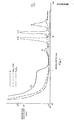
- FIG. 1 is a graphical representation of the absorption coefficient as a function of wavelength, it can be seen that for PSG and silicon dioxide a strong absorption band occurs at wavelengths of about 5 microns and about 9-11 microns, with a peak occurring at about 9.25 microns.
- a CO or a C0 2 laser tuned to this I wavelength was found to be particularly useful in reflowing PSG and silicon dioxide without significantly heating the underlying polysilicon or silicon.
- silicon nitride exhibits a high absorption coefficient for radiation at wavelengths of about 11.5 microns and about 21 microns. iThe laser is therefore tuned to this wavelength for nitride reflow.
- a laser Shaving an emission absorbed by both types of materials is employed.
- the absorption coefficient of both materials is high for wavelengths less than about 400 nm.
- an excimer or other ultraviolet laser having a wavelength less than about 400 nm. will reflow silicon dioxide and heat the adjacent or underlying silicon or polysilicon regions without causing any damage in the silicon or at the silicon to silicon dioxide interface.
- Another aspect of the present invention is embodied in a method for controlling the depth of heating in a layer heated as described above.
- the penetration of laser energy into a particular material that is, the energy intensity at a given distance from the incident surface of the material, may be exnressed as where
- the effective depth of penetration of laser energy into a material for a given I o is approximately (1/ ⁇ ⁇ ).
- a typical energy intensity profile as a function of penetration distance is shown in FIG. 2.
- the depth of heating is further determined by the dwell time in the case of a CW laser and the pulse duration in the case of a pulsed laser.
- the dwell time, t d , of a CW laser is approximately equal to (d/v), where d is the beam diameter and v is the velocity of the laser scan. A shorter dwell time will thus result in a reduced depth of heating for a given CW power at a particular wavelength.
- FIG. 4 shows the depth of heating, which is related to the radiation intensity profiles, for pulses of durations t l and t 2 , where t 2 is less than t l .
- the lateral temperature profile and the associated stresses in a layer of material can be controlled by selecting an appropriate spatial profile for the laser beam.
- a rectangular, a triangular, or any profile other than the normal Gaussian profile may effectively be employed depending on the desired temperature and stress profiles.
- the foregoing embodiments may be effected by a CW laser having a power of about 20-150 watts.
- a spot size ranging from about 50 microns to about 500 microns will result in a power density of about 75-150 kW/cm 2 and, assuming a scan velocity of 0.5-50 cm/sec., the dwell time will range from 0.1-10 msec.
- a satisfactory intensity and temperature profile can be obtained with a pulse duration of about 10 microseconds.
- the resulting energy intensity is about 75-150 kW/cm 2.
- a pulse duration of about 10 nanoseconds at a similar energy level and a pulse repetition rate of 10 3- 10 4 pps. will result in an energy intensity of 75-150 MW/cm 2 .
- the present invention thus provides a method for selectively heating and reflowing an insulating layer in an integrated circuit device without heating an underlying or an adjacent semiconductor layer.
- a method is also provided for simultaneously heating an insulating layer and an underlying semiconductor layer to maintain the integrity of the interface therebetween during reflow of the insulating layer.
Landscapes
- Internal Circuitry In Semiconductor Integrated Circuit Devices (AREA)
- Formation Of Insulating Films (AREA)
Applications Claiming Priority (2)
| Application Number | Priority Date | Filing Date | Title |
|---|---|---|---|
| US442825 | 1982-11-18 | ||
| US06/442,825 US4472456A (en) | 1982-11-18 | 1982-11-18 | Absorption optimized laser annealing |
Publications (3)
| Publication Number | Publication Date |
|---|---|
| EP0109499A2 true EP0109499A2 (fr) | 1984-05-30 |
| EP0109499A3 EP0109499A3 (en) | 1985-07-31 |
| EP0109499B1 EP0109499B1 (fr) | 1988-05-25 |
Family
ID=23758310
Family Applications (1)
| Application Number | Title | Priority Date | Filing Date |
|---|---|---|---|
| EP83109061A Expired EP0109499B1 (fr) | 1982-11-18 | 1983-09-14 | Traitement à laser de PSG, oxyde et nitride via un recuit par laser par absorption sélective optimalisée |
Country Status (4)
| Country | Link |
|---|---|
| US (1) | US4472456A (fr) |
| EP (1) | EP0109499B1 (fr) |
| JP (1) | JPS59103346A (fr) |
| DE (1) | DE3376780D1 (fr) |
Cited By (4)
| Publication number | Priority date | Publication date | Assignee | Title |
|---|---|---|---|---|
| EP0199388A1 (fr) * | 1985-03-29 | 1986-10-29 | Koninklijke Philips Electronics N.V. | Procédé pour la conversion de matériau semi-conducteur polycristallin en matériau semi-conducteur monocristallin |
| EP0268301A3 (en) * | 1986-11-20 | 1989-12-13 | Nec Corporation | Method and apparatus for writing a line on a patterned substrate |
| US9181010B2 (en) | 2010-03-12 | 2015-11-10 | Stora Enso Oyj | Heat-sealable biodegradable packaging material, a method for its manufacture, and a product package made from the material |
| CN120560380A (zh) * | 2025-05-28 | 2025-08-29 | 江苏苏净集团有限公司 | 一种半导体芯片退火设备的高精密温控系统 |
Families Citing this family (8)
| Publication number | Priority date | Publication date | Assignee | Title |
|---|---|---|---|---|
| JPS6014441A (ja) * | 1983-07-04 | 1985-01-25 | Semiconductor Energy Lab Co Ltd | 半導体装置作製方法 |
| US4878097A (en) * | 1984-05-15 | 1989-10-31 | Eastman Kodak Company | Semiconductor photoelectric conversion device and method for making same |
| US4950614A (en) * | 1984-05-15 | 1990-08-21 | Semiconductor Energy Laboratory Co., Ltd. | Method of making a tandem type semiconductor photoelectric conversion device |
| US5094915A (en) * | 1990-05-16 | 1992-03-10 | The Ohio State University | Laser-excited synthesis of carbon films from carbon monoxide-containing gas mixtures |
| US5118923A (en) * | 1991-02-04 | 1992-06-02 | United Technologies Corporation | Laser annealed optical devices made by the proton exchange process |
| US7510961B2 (en) | 1997-02-14 | 2009-03-31 | Micron Technology, Inc. | Utilization of energy absorbing layer to improve metal flow and fill in a novel interconnect structure |
| US6300208B1 (en) | 2000-02-16 | 2001-10-09 | Ultratech Stepper, Inc. | Methods for annealing an integrated device using a radiant energy absorber layer |
| US20040253839A1 (en) * | 2003-06-11 | 2004-12-16 | Tokyo Electron Limited | Semiconductor manufacturing apparatus and heat treatment method |
Family Cites Families (12)
| Publication number | Priority date | Publication date | Assignee | Title |
|---|---|---|---|---|
| US4097889A (en) * | 1976-11-01 | 1978-06-27 | Rca Corporation | Combination glass/low temperature deposited Siw Nx Hy O.sub.z |
| US4258078A (en) * | 1978-06-22 | 1981-03-24 | Bell Telephone Laboratories, Incorporated | Metallization for integrated circuits |
| US4249960A (en) * | 1979-06-18 | 1981-02-10 | Rca Corporation | Laser rounding a sharp semiconductor projection |
| DE2937993A1 (de) * | 1979-09-20 | 1981-04-02 | Siemens AG, 1000 Berlin und 8000 München | Verfahren zum herstellen von integrierten mos-halbleiterschaltungen nach der silizium-gate-technologie |
| DE2943153A1 (de) * | 1979-10-25 | 1981-05-07 | Siemens AG, 1000 Berlin und 8000 München | Verfahren zum herstellen von halbleiterbauelementen mit einer aus phosphorhaltigem siliziumdioxid bestehenden passivierungsschicht |
| JPS5671944A (en) * | 1979-11-19 | 1981-06-15 | Chiyou Lsi Gijutsu Kenkyu Kumiai | Manufacture of semiconductor device |
| JPS56142630A (en) * | 1980-04-09 | 1981-11-07 | Fujitsu Ltd | Manufacture of semiconductor device |
| CA1174285A (fr) * | 1980-04-28 | 1984-09-11 | Michelangelo Delfino | Ecoulement de materiaux structurels de circuits integres obtenu au moyen d'un laser |
| US4284659A (en) * | 1980-05-12 | 1981-08-18 | Bell Telephone Laboratories | Insulation layer reflow |
| JPS5731144A (en) * | 1980-07-31 | 1982-02-19 | Fujitsu Ltd | Mamufacture of semiconductor device |
| JPS5740938A (en) * | 1980-08-26 | 1982-03-06 | Nec Corp | Manufacture of semiconductor device |
| US4474831A (en) * | 1982-08-27 | 1984-10-02 | Varian Associates, Inc. | Method for reflow of phosphosilicate glass |
-
1982
- 1982-11-18 US US06/442,825 patent/US4472456A/en not_active Expired - Lifetime
-
1983
- 1983-09-14 EP EP83109061A patent/EP0109499B1/fr not_active Expired
- 1983-09-14 DE DE8383109061T patent/DE3376780D1/de not_active Expired
- 1983-11-17 JP JP58217067A patent/JPS59103346A/ja active Pending
Cited By (4)
| Publication number | Priority date | Publication date | Assignee | Title |
|---|---|---|---|---|
| EP0199388A1 (fr) * | 1985-03-29 | 1986-10-29 | Koninklijke Philips Electronics N.V. | Procédé pour la conversion de matériau semi-conducteur polycristallin en matériau semi-conducteur monocristallin |
| EP0268301A3 (en) * | 1986-11-20 | 1989-12-13 | Nec Corporation | Method and apparatus for writing a line on a patterned substrate |
| US9181010B2 (en) | 2010-03-12 | 2015-11-10 | Stora Enso Oyj | Heat-sealable biodegradable packaging material, a method for its manufacture, and a product package made from the material |
| CN120560380A (zh) * | 2025-05-28 | 2025-08-29 | 江苏苏净集团有限公司 | 一种半导体芯片退火设备的高精密温控系统 |
Also Published As
| Publication number | Publication date |
|---|---|
| EP0109499B1 (fr) | 1988-05-25 |
| US4472456A (en) | 1984-09-18 |
| EP0109499A3 (en) | 1985-07-31 |
| JPS59103346A (ja) | 1984-06-14 |
| DE3376780D1 (en) | 1988-06-30 |
Similar Documents
| Publication | Publication Date | Title |
|---|---|---|
| KR900000561B1 (ko) | 반도체 집적회로의 제법 및 그를 이용하여 제조된 장치 | |
| EP0037685B1 (fr) | Procédé de fabrication d'un dispositif semiconducteur | |
| US4782029A (en) | Method of gettering semiconductor wafers with an excimer laser beam | |
| US4404735A (en) | Method for manufacturing a field isolation structure for a semiconductor device | |
| KR100696256B1 (ko) | 자외선 레이저 출력으로 전기적인 전도성 링크를 절단하는방법 | |
| KR100804253B1 (ko) | 레이저 섬유 증폭기의 증폭기 출력 제어 방법 | |
| US5405804A (en) | Method of manufacturing a semiconductor device by laser annealing a metal layer through an insulator | |
| US4472456A (en) | Absorption optimized laser annealing | |
| US4443493A (en) | Laser induced flow glass materials | |
| US4379727A (en) | Method of laser annealing of subsurface ion implanted regions | |
| US4390392A (en) | Method for removal of minute physical damage to silicon wafers by employing laser annealing | |
| US4343832A (en) | Semiconductor devices by laser enhanced diffusion | |
| US4249960A (en) | Laser rounding a sharp semiconductor projection | |
| US4549064A (en) | Laser treatment of silicon nitride | |
| JPH0416936B2 (fr) | ||
| US4364778A (en) | Formation of multilayer dopant distributions in a semiconductor | |
| EP0045593A2 (fr) | Procédé pour la fabrication d'un dispositif semi-conducteur | |
| US5139967A (en) | Process for planarizing insulating dielectric material | |
| US4431900A (en) | Laser induced flow Ge-O based materials | |
| Von Allmen et al. | Anisotropic melting and epitaxial regrowth of laser‐irradiated silicon | |
| McMahon et al. | Comparative structural and electrical characterization of scanning‐electron‐and pulsed‐laser‐annealed silicon | |
| US6952269B2 (en) | Apparatus and method for adiabatically heating a semiconductor surface | |
| US4542037A (en) | Laser induced flow of glass bonded materials | |
| JPS641046B2 (fr) | ||
| Brown | Laser processing of semiconductors |
Legal Events
| Date | Code | Title | Description |
|---|---|---|---|
| PUAI | Public reference made under article 153(3) epc to a published international application that has entered the european phase |
Free format text: ORIGINAL CODE: 0009012 |
|
| AK | Designated contracting states |
Designated state(s): DE FR |
|
| PUAL | Search report despatched |
Free format text: ORIGINAL CODE: 0009013 |
|
| AK | Designated contracting states |
Designated state(s): DE FR |
|
| 17P | Request for examination filed |
Effective date: 19860108 |
|
| 17Q | First examination report despatched |
Effective date: 19861218 |
|
| GRAA | (expected) grant |
Free format text: ORIGINAL CODE: 0009210 |
|
| AK | Designated contracting states |
Kind code of ref document: B1 Designated state(s): DE FR |
|
| REF | Corresponds to: |
Ref document number: 3376780 Country of ref document: DE Date of ref document: 19880630 |
|
| ET | Fr: translation filed | ||
| PLBE | No opposition filed within time limit |
Free format text: ORIGINAL CODE: 0009261 |
|
| STAA | Information on the status of an ep patent application or granted ep patent |
Free format text: STATUS: NO OPPOSITION FILED WITHIN TIME LIMIT |
|
| 26N | No opposition filed | ||
| PGFP | Annual fee paid to national office [announced via postgrant information from national office to epo] |
Ref country code: FR Payment date: 20010831 Year of fee payment: 19 |
|
| PGFP | Annual fee paid to national office [announced via postgrant information from national office to epo] |
Ref country code: DE Payment date: 20010927 Year of fee payment: 19 |
|
| PG25 | Lapsed in a contracting state [announced via postgrant information from national office to epo] |
Ref country code: DE Free format text: LAPSE BECAUSE OF NON-PAYMENT OF DUE FEES Effective date: 20030401 |
|
| PG25 | Lapsed in a contracting state [announced via postgrant information from national office to epo] |
Ref country code: FR Free format text: LAPSE BECAUSE OF NON-PAYMENT OF DUE FEES Effective date: 20030603 |
|
| REG | Reference to a national code |
Ref country code: FR Ref legal event code: ST |