EP0045593A2 - Procédé pour la fabrication d'un dispositif semi-conducteur - Google Patents
Procédé pour la fabrication d'un dispositif semi-conducteur Download PDFInfo
- Publication number
- EP0045593A2 EP0045593A2 EP81303366A EP81303366A EP0045593A2 EP 0045593 A2 EP0045593 A2 EP 0045593A2 EP 81303366 A EP81303366 A EP 81303366A EP 81303366 A EP81303366 A EP 81303366A EP 0045593 A2 EP0045593 A2 EP 0045593A2
- Authority
- EP
- European Patent Office
- Prior art keywords
- passivation layer
- laser beam
- semiconductor device
- metallization layers
- process according
- Prior art date
- Legal status (The legal status is an assumption and is not a legal conclusion. Google has not performed a legal analysis and makes no representation as to the accuracy of the status listed.)
- Granted
Links
Images
Classifications
-
- H—ELECTRICITY
- H10—SEMICONDUCTOR DEVICES; ELECTRIC SOLID-STATE DEVICES NOT OTHERWISE PROVIDED FOR
- H10P—GENERIC PROCESSES OR APPARATUS FOR THE MANUFACTURE OR TREATMENT OF DEVICES COVERED BY CLASS H10
- H10P14/00—Formation of materials, e.g. in the shape of layers or pillars
- H10P14/60—Formation of materials, e.g. in the shape of layers or pillars of insulating materials
- H10P14/69—Inorganic materials
- H10P14/692—Inorganic materials composed of oxides, glassy oxides or oxide-based glasses
- H10P14/6921—Inorganic materials composed of oxides, glassy oxides or oxide-based glasses containing silicon
- H10P14/69215—Inorganic materials composed of oxides, glassy oxides or oxide-based glasses containing silicon the material being a silicon oxide, e.g. SiO2
-
- H—ELECTRICITY
- H10—SEMICONDUCTOR DEVICES; ELECTRIC SOLID-STATE DEVICES NOT OTHERWISE PROVIDED FOR
- H10P—GENERIC PROCESSES OR APPARATUS FOR THE MANUFACTURE OR TREATMENT OF DEVICES COVERED BY CLASS H10
- H10P14/00—Formation of materials, e.g. in the shape of layers or pillars
- H10P14/60—Formation of materials, e.g. in the shape of layers or pillars of insulating materials
- H10P14/65—Formation of materials, e.g. in the shape of layers or pillars of insulating materials characterised by treatments performed before or after the formation of the materials
- H10P14/6516—Formation of materials, e.g. in the shape of layers or pillars of insulating materials characterised by treatments performed before or after the formation of the materials of treatments performed after formation of the materials
- H10P14/6536—Formation of materials, e.g. in the shape of layers or pillars of insulating materials characterised by treatments performed before or after the formation of the materials of treatments performed after formation of the materials by exposure to radiation, e.g. visible light
- H10P14/6542—Formation of materials, e.g. in the shape of layers or pillars of insulating materials characterised by treatments performed before or after the formation of the materials of treatments performed after formation of the materials by exposure to radiation, e.g. visible light by using coherent radiation, e.g. using a laser
-
- H—ELECTRICITY
- H10—SEMICONDUCTOR DEVICES; ELECTRIC SOLID-STATE DEVICES NOT OTHERWISE PROVIDED FOR
- H10P—GENERIC PROCESSES OR APPARATUS FOR THE MANUFACTURE OR TREATMENT OF DEVICES COVERED BY CLASS H10
- H10P14/00—Formation of materials, e.g. in the shape of layers or pillars
- H10P14/60—Formation of materials, e.g. in the shape of layers or pillars of insulating materials
- H10P14/69—Inorganic materials
- H10P14/692—Inorganic materials composed of oxides, glassy oxides or oxide-based glasses
- H10P14/6921—Inorganic materials composed of oxides, glassy oxides or oxide-based glasses containing silicon
- H10P14/6922—Inorganic materials composed of oxides, glassy oxides or oxide-based glasses containing silicon the material containing Si, O and at least one of H, N, C, F or other non-metal elements, e.g. SiOC, SiOC:H or SiONC
- H10P14/6923—Inorganic materials composed of oxides, glassy oxides or oxide-based glasses containing silicon the material containing Si, O and at least one of H, N, C, F or other non-metal elements, e.g. SiOC, SiOC:H or SiONC the material being boron or phosphorus doped silicon oxides, e.g. BPSG, BSG or PSG
-
- H—ELECTRICITY
- H10—SEMICONDUCTOR DEVICES; ELECTRIC SOLID-STATE DEVICES NOT OTHERWISE PROVIDED FOR
- H10P—GENERIC PROCESSES OR APPARATUS FOR THE MANUFACTURE OR TREATMENT OF DEVICES COVERED BY CLASS H10
- H10P14/00—Formation of materials, e.g. in the shape of layers or pillars
- H10P14/60—Formation of materials, e.g. in the shape of layers or pillars of insulating materials
- H10P14/69—Inorganic materials
- H10P14/694—Inorganic materials composed of nitrides
- H10P14/6943—Inorganic materials composed of nitrides containing silicon
- H10P14/69433—Inorganic materials composed of nitrides containing silicon the material being a silicon nitride not containing oxygen, e.g. SixNy or SixByNz
-
- H—ELECTRICITY
- H10—SEMICONDUCTOR DEVICES; ELECTRIC SOLID-STATE DEVICES NOT OTHERWISE PROVIDED FOR
- H10P—GENERIC PROCESSES OR APPARATUS FOR THE MANUFACTURE OR TREATMENT OF DEVICES COVERED BY CLASS H10
- H10P34/00—Irradiation with electromagnetic or particle radiation of wafers, substrates or parts of devices
- H10P34/40—Irradiation with electromagnetic or particle radiation of wafers, substrates or parts of devices with high-energy radiation
- H10P34/42—Irradiation with electromagnetic or particle radiation of wafers, substrates or parts of devices with high-energy radiation with electromagnetic radiation, e.g. laser annealing
-
- H—ELECTRICITY
- H10—SEMICONDUCTOR DEVICES; ELECTRIC SOLID-STATE DEVICES NOT OTHERWISE PROVIDED FOR
- H10P—GENERIC PROCESSES OR APPARATUS FOR THE MANUFACTURE OR TREATMENT OF DEVICES COVERED BY CLASS H10
- H10P95/00—Generic processes or apparatus for manufacture or treatments not covered by the other groups of this subclass
-
- H—ELECTRICITY
- H10—SEMICONDUCTOR DEVICES; ELECTRIC SOLID-STATE DEVICES NOT OTHERWISE PROVIDED FOR
- H10P—GENERIC PROCESSES OR APPARATUS FOR THE MANUFACTURE OR TREATMENT OF DEVICES COVERED BY CLASS H10
- H10P14/00—Formation of materials, e.g. in the shape of layers or pillars
- H10P14/60—Formation of materials, e.g. in the shape of layers or pillars of insulating materials
- H10P14/63—Formation of materials, e.g. in the shape of layers or pillars of insulating materials characterised by the formation processes
- H10P14/6326—Deposition processes
- H10P14/6328—Deposition from the gas or vapour phase
- H10P14/6329—Deposition from the gas or vapour phase using physical ablation of a target, e.g. physical vapour deposition or pulsed laser deposition
-
- H—ELECTRICITY
- H10—SEMICONDUCTOR DEVICES; ELECTRIC SOLID-STATE DEVICES NOT OTHERWISE PROVIDED FOR
- H10P—GENERIC PROCESSES OR APPARATUS FOR THE MANUFACTURE OR TREATMENT OF DEVICES COVERED BY CLASS H10
- H10P14/00—Formation of materials, e.g. in the shape of layers or pillars
- H10P14/60—Formation of materials, e.g. in the shape of layers or pillars of insulating materials
- H10P14/63—Formation of materials, e.g. in the shape of layers or pillars of insulating materials characterised by the formation processes
- H10P14/6326—Deposition processes
- H10P14/6328—Deposition from the gas or vapour phase
- H10P14/6334—Deposition from the gas or vapour phase using decomposition or reaction of gaseous or vapour phase compounds, i.e. chemical vapour deposition
- H10P14/6336—Deposition from the gas or vapour phase using decomposition or reaction of gaseous or vapour phase compounds, i.e. chemical vapour deposition in the presence of a plasma [PECVD]
-
- Y—GENERAL TAGGING OF NEW TECHNOLOGICAL DEVELOPMENTS; GENERAL TAGGING OF CROSS-SECTIONAL TECHNOLOGIES SPANNING OVER SEVERAL SECTIONS OF THE IPC; TECHNICAL SUBJECTS COVERED BY FORMER USPC CROSS-REFERENCE ART COLLECTIONS [XRACs] AND DIGESTS
- Y10—TECHNICAL SUBJECTS COVERED BY FORMER USPC
- Y10S—TECHNICAL SUBJECTS COVERED BY FORMER USPC CROSS-REFERENCE ART COLLECTIONS [XRACs] AND DIGESTS
- Y10S438/00—Semiconductor device manufacturing: process
- Y10S438/958—Passivation layer
Definitions
- the present invention relates to a process for producing a semiconductor device, particularly a process comprising a step of forming a passivation layer which is deposited on the surface of a device and which covers metallization layers thereof.
- a semiconductor device such as an integrated circuit has usually a passivation layer on the surface thereof so as to avoid undesirable penetration of moisture and/or cations such as sodium ions from the environment. Therefore, the passivation layer must not be porous even in microsize.
- the passivation layer is usually made of silicon nitride or silicon oxide or phosphorus silicate glass and is formed on the metallization layers which are composed mainly of aluminium. This metal has a tendency to deform at a temperature above 450°C. Therefore, the passivation layer must be deposited at a temperature lower than 450°C.
- the passivation layer is usually formed by vapour phase deposition. Its deposition temperature varies depending on the type of the deposited composition, e.g., for silicon nitride about 850°C, for silicon oxide about 400°C and for phosphorous silicate glass about 400 450°C. In order to satisfy the above-mentioned low temperature deposition, recently a silicon nitride passivation layer has been formed by plasma vapour phase deposition which is capable of depositing at about 300 about 400°C.
- the passivation layer must not be heated at a temperature higher than 450°C during both the depositing of the layer and the processing of it after its formation, and, simultaneously, the thus formed passivation layer must not be porous and must not occlude hydrogen gas in its pores and must not contain hydrogen atoms in a combined state with the atoms which constitute the material of the layer.
- an instantaneous laser irradiation is used as annealing in which only the very surface of a material is heated upto a high temperature and is rapidly cooled after the irradiation ceases.
- a semiconductor device is instantaneously irradiated by a laser beam after the process of ion implantation in its source and drain regions so as to eliminate defects in the crystal.
- Such a laser beam annealing has the advantage of maintaining the impurity profile in source and drain regions formed with a controlled accuracy, which might deteriorate if the device was heated in a heating vessel for a long period.
- a passivation layer is deposited after processing several steps so as to complete the fabrication of semiconductor elements and also metallization layers after the step of ion implantation.
- a process for producing a semiconductor device characterized by comprising a step of annealing a porous passivation layer which is deposited on the surface of said device and which covers metallization layers fabricated thereon by irradiating a laser beam on said passivation layer so as to densify said passivation layer, while said laser beam scans the surface of said passivation layer.
- the laser beam may be a continuous beam or a pulsed beam.
- the laser beam can be generated by a YAG, ruby, argon or carbon dioxide laser.
- the passivation layer may be made from silicon nitride or silicon oxide or phosphorous silicate glass.
- the metallization layers may be composed mainly of aluminium.
- the metallization layers may be composed of aluminium containing a small amount of silicon or copper.
- a silicon oxide field layer 2 which isolates transistors from one another, ion-implanted source and drain regions 3 and 4, a polysilicon gate electrode 5, a phosphorus silicate glass layer 6, an aluminium metallization layer 7 and silicon nitride passivation layers 8.
- the silicon oxide field layer 2 has a dense structure, because it is oxidized at about 1000°C for a relatively long period.
- the silicon nitride passivation layers 8 are porous because they are formed by plasma vapour phase deposition at about 350°C in order to avoid the deformation of the metallization layer 7.
- a continuous argon laser beam of 5 W having wave lengths of 488 and 514 nm was generated.
- the argon laser beam about 30 ⁇ about 40 ⁇ m in diameter was irradiated on the passivation layer with a scanning speed of 4 inch/sec.
- the surface of the passivation layer was instantaneously heated upto about 600°C and then rapidly cooled.
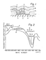
- Fig. 2 illustrates two absorption spectra, curve A exhibits the absorption characteristics of the passivation layer before the laser beam scanning, and curve B exhibits its behavior after the laser beam scanning. Absorption peaks are shown in these curves.
- a large peak of Si-N bond (820 cm -1 ) is recognized in both curves.
- N-H bond (3300 cm -1 ).
- Si-H bond (2200 cm 1 ) and Si- N (- H )- S i (1200 cm- 1 ) disappear in the curve B of annealed layer. The disappearance of these H-bonds reveals that hydrogen has been completely removed from the passivation layer.
- the silicon nitride passivation layer was immersed in saturated hydrofluoric acid, before and after the laser beam scanning.
- the etching rate decreased from 0 0
- the underlying aluminium metallization layer does not fuse, and, therefore, its pattern does not deteriorate.
Landscapes
- Formation Of Insulating Films (AREA)
Applications Claiming Priority (2)
| Application Number | Priority Date | Filing Date | Title |
|---|---|---|---|
| JP105910/80 | 1980-07-31 | ||
| JP10591080A JPS5731144A (en) | 1980-07-31 | 1980-07-31 | Mamufacture of semiconductor device |
Publications (3)
| Publication Number | Publication Date |
|---|---|
| EP0045593A2 true EP0045593A2 (fr) | 1982-02-10 |
| EP0045593A3 EP0045593A3 (en) | 1982-09-29 |
| EP0045593B1 EP0045593B1 (fr) | 1985-03-20 |
Family
ID=14420012
Family Applications (1)
| Application Number | Title | Priority Date | Filing Date |
|---|---|---|---|
| EP81303366A Expired EP0045593B1 (fr) | 1980-07-31 | 1981-07-23 | Procédé pour la fabrication d'un dispositif semi-conducteur |
Country Status (4)
| Country | Link |
|---|---|
| US (1) | US4406053A (fr) |
| EP (1) | EP0045593B1 (fr) |
| JP (1) | JPS5731144A (fr) |
| DE (1) | DE3169377D1 (fr) |
Cited By (4)
| Publication number | Priority date | Publication date | Assignee | Title |
|---|---|---|---|---|
| EP0109499A3 (en) * | 1982-11-18 | 1985-07-31 | Texas Instruments Incorporated | Laser processing of psg, oxide and nitride via absorption optimized selective laser annealing |
| GB2266181A (en) * | 1992-03-31 | 1993-10-20 | Mitsubishi Electric Corp | Semiconductor integrated circuit with an insulating layer incorporating vacancies |
| KR101185990B1 (ko) * | 2010-12-20 | 2012-09-25 | 에스케이하이닉스 주식회사 | 반도체 소자의 형성방법 |
| EP1676300B1 (fr) * | 2003-10-03 | 2014-10-01 | Applied Materials, Inc. | Procede de recuit d'un substrat avec une couche absorbante |
Families Citing this family (11)
| Publication number | Priority date | Publication date | Assignee | Title |
|---|---|---|---|---|
| US4566913A (en) * | 1984-07-30 | 1986-01-28 | International Business Machines Corporation | Rapid thermal annealing of silicon dioxide for reduced electron trapping |
| US5010024A (en) * | 1987-03-04 | 1991-04-23 | Advanced Micro Devices, Inc. | Passivation for integrated circuit structures |
| US5264724A (en) * | 1989-02-13 | 1993-11-23 | The University Of Arkansas | Silicon nitride for application as the gate dielectric in MOS devices |
| JPH0370178A (ja) * | 1989-08-09 | 1991-03-26 | Seiko Instr Inc | 半導体装置 |
| JP3277533B2 (ja) * | 1992-01-08 | 2002-04-22 | ソニー株式会社 | 半導体装置の製造方法 |
| US5472913A (en) * | 1994-08-05 | 1995-12-05 | Texas Instruments Incorporated | Method of fabricating porous dielectric material with a passivation layer for electronics applications |
| TW388095B (en) * | 1997-05-20 | 2000-04-21 | United Microelectronics Corp | Method for improving planarization of dielectric layer in interconnect metal process |
| US7112545B1 (en) | 1999-09-10 | 2006-09-26 | The Board Of Trustees Of The University Of Arkansas | Passivation of material using ultra-fast pulsed laser |
| WO2001018852A1 (fr) * | 1999-09-10 | 2001-03-15 | The Board Of Trustees Of The University Of Arkansas | Passivation de materiau par laser a impulsions ultra-rapides |
| US20050127475A1 (en) * | 2003-12-03 | 2005-06-16 | International Business Machines Corporation | Apparatus and method for electronic fuse with improved esd tolerance |
| CN118006877A (zh) * | 2023-12-26 | 2024-05-10 | 佛山科学技术学院 | 一种增强高熵合金耐腐蚀性的复合系统及其使用方法 |
Family Cites Families (10)
| Publication number | Priority date | Publication date | Assignee | Title |
|---|---|---|---|---|
| NL87258C (fr) * | 1969-01-15 | |||
| BE788682A (fr) * | 1971-09-13 | 1973-03-12 | Westinghouse Electric Corp | Systeme de fixation et de liberation de couvercle superieur de cuve de reacteur |
| US3881971A (en) * | 1972-11-29 | 1975-05-06 | Ibm | Method for fabricating aluminum interconnection metallurgy system for silicon devices |
| US4015100A (en) * | 1974-01-07 | 1977-03-29 | Avco Everett Research Laboratory, Inc. | Surface modification |
| US4059461A (en) * | 1975-12-10 | 1977-11-22 | Massachusetts Institute Of Technology | Method for improving the crystallinity of semiconductor films by laser beam scanning and the products thereof |
| JPS5280779A (en) * | 1975-12-27 | 1977-07-06 | Fujitsu Ltd | Production of simiconductor device |
| US4229232A (en) * | 1978-12-11 | 1980-10-21 | Spire Corporation | Method involving pulsed beam processing of metallic and dielectric materials |
| JPS561533A (en) * | 1979-06-18 | 1981-01-09 | Hitachi Ltd | Method of photoetching |
| DE2943153A1 (de) * | 1979-10-25 | 1981-05-07 | Siemens AG, 1000 Berlin und 8000 München | Verfahren zum herstellen von halbleiterbauelementen mit einer aus phosphorhaltigem siliziumdioxid bestehenden passivierungsschicht |
| US4284659A (en) * | 1980-05-12 | 1981-08-18 | Bell Telephone Laboratories | Insulation layer reflow |
-
1980
- 1980-07-31 JP JP10591080A patent/JPS5731144A/ja active Pending
-
1981
- 1981-07-23 DE DE8181303366T patent/DE3169377D1/de not_active Expired
- 1981-07-23 EP EP81303366A patent/EP0045593B1/fr not_active Expired
- 1981-07-31 US US06/289,296 patent/US4406053A/en not_active Expired - Fee Related
Cited By (6)
| Publication number | Priority date | Publication date | Assignee | Title |
|---|---|---|---|---|
| EP0109499A3 (en) * | 1982-11-18 | 1985-07-31 | Texas Instruments Incorporated | Laser processing of psg, oxide and nitride via absorption optimized selective laser annealing |
| GB2266181A (en) * | 1992-03-31 | 1993-10-20 | Mitsubishi Electric Corp | Semiconductor integrated circuit with an insulating layer incorporating vacancies |
| GB2266181B (en) * | 1992-03-31 | 1995-08-23 | Mitsubishi Electric Corp | Semiconductor integrated circuit and method for producing the semiconductor integrated circuit |
| US5468685A (en) * | 1992-03-31 | 1995-11-21 | Mitsubishi Denki Kabushiki Kaisha | Method for producing a semiconductor integrated circuit |
| EP1676300B1 (fr) * | 2003-10-03 | 2014-10-01 | Applied Materials, Inc. | Procede de recuit d'un substrat avec une couche absorbante |
| KR101185990B1 (ko) * | 2010-12-20 | 2012-09-25 | 에스케이하이닉스 주식회사 | 반도체 소자의 형성방법 |
Also Published As
| Publication number | Publication date |
|---|---|
| JPS5731144A (en) | 1982-02-19 |
| DE3169377D1 (en) | 1985-04-25 |
| EP0045593A3 (en) | 1982-09-29 |
| US4406053A (en) | 1983-09-27 |
| EP0045593B1 (fr) | 1985-03-20 |
Similar Documents
| Publication | Publication Date | Title |
|---|---|---|
| US4404735A (en) | Method for manufacturing a field isolation structure for a semiconductor device | |
| EP0045593B1 (fr) | Procédé pour la fabrication d'un dispositif semi-conducteur | |
| US4468855A (en) | Method of making aluminum gate self-aligned FET by selective beam annealing through reflective and antireflective coatings | |
| JP4295922B2 (ja) | 小型集積回路の作製における用途に適したガス浸漬レーザアニーリング方法 | |
| US5324974A (en) | Nitride capped MOSFET for integrated circuits | |
| EP0008928B1 (fr) | Procédé pour la fabrication d'un dispositif semi-conducteur | |
| US5405804A (en) | Method of manufacturing a semiconductor device by laser annealing a metal layer through an insulator | |
| JPS6359251B2 (fr) | ||
| JPS5955054A (ja) | 半導体装置の製造方法 | |
| US5225357A (en) | Low P+ contact resistance formation by double implant | |
| US6909154B2 (en) | Sacrificial annealing layer for a semiconductor device and a method of fabrication | |
| JPH0368133A (ja) | 固相拡散方法 | |
| Stein | Thermal Annealing of Si‐N Absorption Bands in Nitrogen‐Implanted Silicon | |
| GB2307790A (en) | Method of removing defects from semiconductor devices. | |
| JPH06204248A (ja) | Misトランジスタの作製方法 | |
| JPS6250971B2 (fr) | ||
| US5759869A (en) | Method to imporve metal step coverage by contact reflow | |
| JPS6161268B2 (fr) | ||
| JP3370029B2 (ja) | 半導体装置の作製方法 | |
| JPH0336312B2 (fr) | ||
| JPH022633A (ja) | Mis電界効果半導体装置の製造方法 | |
| JP3387862B2 (ja) | 半導体装置の作製方法 | |
| JPS621269B2 (fr) | ||
| KR100192168B1 (ko) | 반도체 소자의 다층 금속 배선 형성방법 | |
| KR100400781B1 (ko) | 피모스 반도체 소자의 제조방법 |
Legal Events
| Date | Code | Title | Description |
|---|---|---|---|
| PUAI | Public reference made under article 153(3) epc to a published international application that has entered the european phase |
Free format text: ORIGINAL CODE: 0009012 |
|
| AK | Designated contracting states |
Designated state(s): DE FR GB NL |
|
| RBV | Designated contracting states (corrected) |
Designated state(s): DE FR GB NL |
|
| PUAL | Search report despatched |
Free format text: ORIGINAL CODE: 0009013 |
|
| AK | Designated contracting states |
Designated state(s): DE FR GB NL |
|
| 17P | Request for examination filed |
Effective date: 19821209 |
|
| GRAA | (expected) grant |
Free format text: ORIGINAL CODE: 0009210 |
|
| AK | Designated contracting states |
Designated state(s): DE FR GB NL |
|
| REF | Corresponds to: |
Ref document number: 3169377 Country of ref document: DE Date of ref document: 19850425 |
|
| ET | Fr: translation filed | ||
| PLBI | Opposition filed |
Free format text: ORIGINAL CODE: 0009260 |
|
| PLBI | Opposition filed |
Free format text: ORIGINAL CODE: 0009260 |
|
| 26 | Opposition filed |
Opponent name: SIEMENS AKTIENGESELLSCHAFT, BERLIN UND MUENCHEN Effective date: 19851217 |
|
| NLR1 | Nl: opposition has been filed with the epo |
Opponent name: SIEMENS AKTIENGESELLSCHAFT |
|
| 26 | Opposition filed |
Opponent name: TELEFUNKEN ELECTRONIC GMBH Effective date: 19851220 |
|
| NLR1 | Nl: opposition has been filed with the epo |
Opponent name: TELEFUNKEN ELECTRONIC GMBH |
|
| PGFP | Annual fee paid to national office [announced via postgrant information from national office to epo] |
Ref country code: NL Payment date: 19870731 Year of fee payment: 7 |
|
| PGFP | Annual fee paid to national office [announced via postgrant information from national office to epo] |
Ref country code: GB Payment date: 19890630 Year of fee payment: 9 |
|
| RDAG | Patent revoked |
Free format text: ORIGINAL CODE: 0009271 |
|
| STAA | Information on the status of an ep patent application or granted ep patent |
Free format text: STATUS: PATENT REVOKED |
|
| 27W | Patent revoked |
Effective date: 19890223 |
|
| GBPR | Gb: patent revoked under art. 102 of the ep convention designating the uk as contracting state | ||
| NLR2 | Nl: decision of opposition | ||
| APAH | Appeal reference modified |
Free format text: ORIGINAL CODE: EPIDOSCREFNO |