EP0110301A2 - Methode und Gerät zur Grössenmessung eines Sekundärelektronen emittierenden Objektes - Google Patents
Methode und Gerät zur Grössenmessung eines Sekundärelektronen emittierenden Objektes Download PDFInfo
- Publication number
- EP0110301A2 EP0110301A2 EP83111669A EP83111669A EP0110301A2 EP 0110301 A2 EP0110301 A2 EP 0110301A2 EP 83111669 A EP83111669 A EP 83111669A EP 83111669 A EP83111669 A EP 83111669A EP 0110301 A2 EP0110301 A2 EP 0110301A2
- Authority
- EP
- European Patent Office
- Prior art keywords
- sample
- reference points
- accordance
- image
- scanning
- Prior art date
- Legal status (The legal status is an assumption and is not a legal conclusion. Google has not performed a legal analysis and makes no representation as to the accuracy of the status listed.)
- Granted
Links
- 238000000034 method Methods 0.000 title claims description 35
- 238000010894 electron beam technology Methods 0.000 claims description 15
- 230000001186 cumulative effect Effects 0.000 claims 3
- 239000004065 semiconductor Substances 0.000 description 23
- 235000012431 wafers Nutrition 0.000 description 20
- 238000005259 measurement Methods 0.000 description 19
- 229910052782 aluminium Inorganic materials 0.000 description 15
- XAGFODPZIPBFFR-UHFFFAOYSA-N aluminium Chemical compound [Al] XAGFODPZIPBFFR-UHFFFAOYSA-N 0.000 description 15
- 238000007796 conventional method Methods 0.000 description 11
- 238000012545 processing Methods 0.000 description 11
- XUIMIQQOPSSXEZ-UHFFFAOYSA-N Silicon Chemical compound [Si] XUIMIQQOPSSXEZ-UHFFFAOYSA-N 0.000 description 5
- 229910052710 silicon Inorganic materials 0.000 description 5
- 239000010703 silicon Substances 0.000 description 5
- 239000000758 substrate Substances 0.000 description 5
- 238000009825 accumulation Methods 0.000 description 4
- 238000004364 calculation method Methods 0.000 description 4
- 230000003287 optical effect Effects 0.000 description 3
- 229910052581 Si3N4 Inorganic materials 0.000 description 2
- 238000006243 chemical reaction Methods 0.000 description 2
- 238000010586 diagram Methods 0.000 description 2
- 229910052751 metal Inorganic materials 0.000 description 2
- 239000002184 metal Substances 0.000 description 2
- 238000012856 packing Methods 0.000 description 2
- 229920002120 photoresistant polymer Polymers 0.000 description 2
- 229910021420 polycrystalline silicon Inorganic materials 0.000 description 2
- 229920005591 polysilicon Polymers 0.000 description 2
- 230000004044 response Effects 0.000 description 2
- HQVNEWCFYHHQES-UHFFFAOYSA-N silicon nitride Chemical compound N12[Si]34N5[Si]62N3[Si]51N64 HQVNEWCFYHHQES-UHFFFAOYSA-N 0.000 description 2
- 238000012935 Averaging Methods 0.000 description 1
- 229910000905 alloy phase Inorganic materials 0.000 description 1
- 238000004458 analytical method Methods 0.000 description 1
- 239000000919 ceramic Substances 0.000 description 1
- 239000000571 coke Substances 0.000 description 1
- 239000013078 crystal Substances 0.000 description 1
- 238000011161 development Methods 0.000 description 1
- 238000006073 displacement reaction Methods 0.000 description 1
- 238000005530 etching Methods 0.000 description 1
- 230000006870 function Effects 0.000 description 1
- 238000004519 manufacturing process Methods 0.000 description 1
- 239000011159 matrix material Substances 0.000 description 1
- 230000006386 memory function Effects 0.000 description 1
- 239000002245 particle Substances 0.000 description 1
- 238000000059 patterning Methods 0.000 description 1
- 239000011148 porous material Substances 0.000 description 1
- 239000000843 powder Substances 0.000 description 1
- 238000005070 sampling Methods 0.000 description 1
- 238000003860 storage Methods 0.000 description 1
- 230000001131 transforming effect Effects 0.000 description 1
- 239000011800 void material Substances 0.000 description 1
Images




Classifications
-
- H—ELECTRICITY
- H01—ELECTRIC ELEMENTS
- H01J—ELECTRIC DISCHARGE TUBES OR DISCHARGE LAMPS
- H01J37/00—Discharge tubes with provision for introducing objects or material to be exposed to the discharge, e.g. for the purpose of examination or processing thereof
- H01J37/26—Electron or ion microscopes; Electron or ion diffraction tubes
- H01J37/28—Electron or ion microscopes; Electron or ion diffraction tubes with scanning beams
-
- G—PHYSICS
- G01—MEASURING; TESTING
- G01B—MEASURING LENGTH, THICKNESS OR SIMILAR LINEAR DIMENSIONS; MEASURING ANGLES; MEASURING AREAS; MEASURING IRREGULARITIES OF SURFACES OR CONTOURS
- G01B15/00—Measuring arrangements characterised by the use of electromagnetic waves or particle radiation, e.g. by the use of microwaves, X-rays, gamma rays or electrons
-
- G—PHYSICS
- G01—MEASURING; TESTING
- G01B—MEASURING LENGTH, THICKNESS OR SIMILAR LINEAR DIMENSIONS; MEASURING ANGLES; MEASURING AREAS; MEASURING IRREGULARITIES OF SURFACES OR CONTOURS
- G01B7/00—Measuring arrangements characterised by the use of electric or magnetic techniques
- G01B7/02—Measuring arrangements characterised by the use of electric or magnetic techniques for measuring length, width or thickness
Definitions
- the present invention relates to a method and apparatus for automatically measuring a dimension of an object onto which electron beam is radiated and which emits secondary electron with high precision.
- a conventional method and apparatus for measuring a small dimension or size includes a dimension of crystals of a metal, a dimension of an subgrain boundry, a dimension of a non-metallic inclusion in a metal, a dimension of an alloy phase, a powder particle size, a dimension of an IC mask pattern, a size of a CRT spot, a dimension of an insulating ceramic, a dimension of a color TV shadow mask, a pore size and a void size of an electrode coke, a gap dimension of a magnetic core, a gap dimension of a magnetic head and the like.
- An example of a pattern formed on a semiconductor wafer will be described hereinafter.
- a conventional method for measuring a width of a photoresist pattern, a polysilicon pattern, a silicon nitride pattern and any other various types of pattern formed on semiconductor wafer an image of a pattern as an object to be measured is optically enlarged and measured using a micrometer with an optical microscope, electronic measuring equipment combining an industrial television and an optical microscope, or the like.
- a laser beam is irradiated onto a semiconductor wafer using a device comprising a combination of a laser and a precision-movable stage, and a width of a pattern is measured by measuring the intensity of reflected light and the amount of displacement of the stage.
- an enlarged image of a pattern of a semiconductor wafer is measured using a scale, and the width of the pattern is determined from the obtained measurement and the magnification of the SEM during the measurement.
- Still another conventional method is also known wherein an enlarged image of a pattern is divided into a plurality of picture elements, cursors are generated on a screen, the operator aligns the cursors at the edges of the pattern on the screen, and the dimension of the pattern to be measured is determined from the number of picture elements between the cursors and the magnification of the SEM.
- Still another conventional method is also described in Japanese Patent Disclosure No. 56-105633.
- a signal obtained from the SEM and corresponding to the semiconductor wafer is compared with a critical discrimination level (threshold level).
- Threshold level a critical discrimination level
- a point at which these two level coincide is determined to determine the width of a pattern to be measured.
- a higher resolution of a device for measuring a width of a semiconductor pattern is required. More specifically, a resolution of 0.1 ⁇ m or greater is required.
- the magnification is limited and limitation of the resolution is about 1/4 the wavelength, both being unsatisfactory.
- the present invention has been made in consideration of this and has for its object to provide a method and apparatus for automatically measuring a small dimension of an object to be measured with high precision.
- a method for measuring the dimensions of an object included in a sample comprising the steps of:
- an apparatus for measuring the dimensions of the object included in a sample comprising:
- the method or apparatus of the present invention When the method or apparatus of the present invention is applied to the checking of LSIs or VLSIs, checking can be performed with high reliability and with ease. As a result, semiconductor devices of a better quality can be manufactured at a higher yield.
- the method and apparatus of the present invention thus significantly contribute to the development of various manufacturing techniques for higher packing density and the determination of process conditions. The same applies to measurements of objects other than a pattern formed on a semiconductor wafer.
- Fig. 1 is a block diagram showing the configuration of a dimension measuring apparatus according to an embodiment of the present invention.
- the apparatus shown in Fig. 1 consists of a scanning electron microscope (SEM) main body 1, and a dimension measuring section 2 for measuring a dimension of a specific portion of a sample to be measured in accordance with data obtained from the SEM main body 1.
- SEM scanning electron microscope
- the SEM main body 1 has the following configuration. More specifically, the SEM main body 1 has an electron gun 3 for emitting an electron beam 4. A condenser lens 5 reduces the diameter of the electron beam 4 emitted from the electron gun 3.
- the SEM main body 1 also has a reference signal generator 6 for generating a clock signal PS. In accordance with the clock signal PS from the reference signal generator 6, a sweep signal generator 7 generates a sweep signal SS for raster scanning the electron beam 4.
- a magnification selector 9 produces a control signal CS1 for controlling a scanning coil 8 by combining the sweep signal SS and a magnification signal from a magnification selection switch (not shown).
- the control signal CS1 is supplied to a CPU section 16 to be described later.
- the scanning coil 8 controls the scanning direction and width of the electron beam 4.
- the diameter of the electron beam 4 is further reduced by an objective lens 11, and the size-reduced electron beam 4 is radiated onto a semiconductor wafer 10.
- a secondary electron detector 12 detects the secondary electrons and supplies to an amplifier 13 a signal SE corresponding to the amount of the detected secondary electrons.
- the amplifier 13 amplifies the signal SE and supplies amplified signal SE as a signal IS to an image signal amplifier 15.
- the image signal amplifier 15 supplies a signal to a cathode ray tube (CRT) 14. In accordance with the signal from the image signal amplifier 15, the C RT 14 displays an enlarged image of the specific portion of the semiconductor wafer 10.
- CTR cathode ray tube
- the dimension measuring section 2 has a configuration as described below. More specifically, the dimen- sionmeasuring section 2 has the CPU section 16 which produces a control signal CS2 for controlling the operation of an A/D converter 17 in accordance with the clock signal PS from the reference signal generator 6 and the sweep signal SS from the sweep signal generator 7.
- the CPU section 16 has a CPU, a RAM, a ROM and the like, and has an arithmetic function and a memory function to be described later.
- the A/D converter 17 In response to the control signal CS2 from the CPU section 16, the A/D converter 17 converts an image signal IS from an amplifier 13 into divided image signals corresponding to a plurality of picture elements (512 x 512). The A/D converter 17 further converts the image signal IS, assigns addresses to the divided image signals, and produces resultant digital image signals DIS.
- the digital image signals DIS are obtained by sampling the image signal IS at timings determined by the control signal CS2 from the CPU section 16, and performing A/D conversion.
- a memory 18 stores the obtained digital image signals DIS.
- the dimension measuring section 2 also has a cursor setter 19 for producing a cursor signal KS.
- the cursor signal KS is supplied to the CRT 14 through the image signal amplifier 15 to generate cursors on the C R T 14 and to move the displayed cursors.
- Setting and moving of the cursors can be performed with a cursor setter having a known joystick circuit (not shown) and a comparator, by generating a voltage from the joystick circuit and changing a point at which the voltage from the joystick circuit coincides with the voltage of the sweep signal SS from the sweep signal generator 7.
- a cursor reader 20 reads the positions of the cursors on the CRT 14 and produces address signals AS.
- the address signals AS are supplied to the CPU section 16 together with the clock signal PS, the sweep signal SS, and the control signal C Sl from the magnification selector 9.
- the CPU section 16 performs various types of processing and storage to be described later in accordance with these signals.
- the arithmetic results obtained by the CPU section 16 are supplied to a D/A converter 21.
- the D/A converter 21 D/A converts the received arithmetic results from the CPU section 16 to an analog signal, and the obtained results are displayed at the CRT 14 through the image signal amplifier 15.
- the semiconductor wafer 10 consisting of the silicon substrate 25 and the aluminum pattern 27 is placed on the table of the SEM main body 1.
- Fig. 2 shows a section of the semiconductor wafer 10.
- the electron beam 4 emitted from the electron gun 3 is reduced in diameter by the condenser lens 5 and is raster-scanned in the X-Y directions by the scanning coil 8 in accordance with the control signal CSl from the magnification selector 9.
- the electron beam 4 is further reduced in diameter by the objective lens 11 and is irradiated onto the semiconductor wafer 10.
- the silicon substrate 25 and the aluminum pattern 27 of the semiconductor wafer 10 emit secondary electrons at different rates.
- the emitted secondary electrons are detected by the secondary electron detector 12 and are converted into electrical signals S E .
- the electrical signals SE from the secondary electron detector 12 are amplified by the amplifier 13 and are supplied to the image signal amplifier 15 as the image signals IS.
- the image signals IS from the amplifier 13 and the sweep signal SS from the sweep signal generator 7 are combined by the image signal amplifier 15 and are supplied to the CRT 14.
- the CRT 14 displays an enlarged image (Fig. 3) of a specific portion of the semiconductor wafer 10 in accordance with the output signals from the image signal amplifier 15.
- the screen of the CRT 14 is divided into a matrix of 512 x 512 picture elements by raster scanning (along the direction indicated by arrow A in Fig. 4) and scanning line division (along the direction indicated by arrow B in Fig. 4).
- Each picture element is assigned an address IS (i, j) (0 ⁇ i, j ⁇ 511), as shown in Fig. 4.
- the image signals IS from the amplifier 13 are sampled by the A/D converter 17 at a timing which is designated by the control signal CS2 from the CPU section 16, and are then divided into signals corresponding to the respective picture elements.
- the divided signals are assigned addresses I S(i, j) (0 ⁇ i, j ⁇ 511), which is corresponding to the addresses of picture elements on the screen of the CRT 14, and are A/D converted.
- the resultant digital image signals DIS are stored in the memory 18.
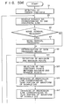
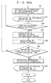
- the step of measuring a width D of the aluminum pattern 27 of the semiconductor wafer in accordance with the enlarged image of the semiconductor wafer 10 displayed on the CRT 14 and various signals will be described with reference to the flow charts shown in Figs. 5(a) and 5(b).
- the cursor setter 19 moves two cursors 31a and 31b to positions sandwiching the aluminum pattern 27 therebetween, as shown in Fig. 3.
- a distance W between the two cursors 31a and 31b and a length L of each cursor 31a or 31b can be adjusted at the cursor setter 19.
- the CPU section 16 detects the positions of the cursors 31a and 31b on the CRT 14 in accordance with the address signal AS from the cursor reader 20 (step Sl). Then, a region for data processing is determined (a hatched region shown in Fig. 3).
- the CPU section 16 receives from the memory 18 the digital image signals DIS of one horizontal line within the region defined by the length of the cursors 31a and 31b (step S3).
- the one line digital image signals are subjected to noise removal processing by the FFT method or ARC (Accumulation Ramp Conversion) method to be described later, as needed (steps S5 and S7).
- the signals DIS obtained by such noise removal are shown in Fig. 6.
- the portion corresponding to the silicon substrate 25 of the semiconductor wafer 10 has a low voltage
- the portion corresponding to the aluminum pattern 27 has a high voltage.
- the region to be processed and designated by the cursors 31a and 31b is determined (step S9).
- the data processing region is indicated by arrow X in Fig. 6.
- portions 41 and 43 of the signal DIS within the data processing region correspond to the edge portions of the aluminum pattern 27.
- Fig. 7 shows an enlarged view of a portion surrounding the portion 41.
- a point 51 of maximum value and a point 53 of minimum value in the vicinity of the portion 41 are detected (step Sll).
- Two arbitrary points 55 and 57 between the points 51 and 53 are selected (step S13).
- the point 55 is selected to be a point at which the signal level is 80% of the maximum value
- the point 57 is selected to be a point at which the signal level is 30% of the maximum value.
- a regression line 59 is obtained by the method of least squares in accordance with the data between the points 55 and 57, that is, the data of the signal ramp portion (step S15).
- a regression line 61 for the data between the points 53 and 57, that is, the data corresponding to the flat portion of the signal waveform, is obtained by the method of least squares (step S17).
- An intersection 63 of the regression lines 59 and 61 is obtained (step S19). This intersection 63 is given as one reference point.
- the data of the reference point 63 is supplied to the D/A converter 21 and is displayed on the CRT 14 (step S21). The same data is also stored in the memory 18.
- regression lines 65 and 67 are obtained for the portion 43 (steps S23, Sll to S17).
- An intersection 69 of the regression lines 65 and 67 is calculated (step S19).
- the intersection 69 is defined as the other reference point for dimension measurement.
- the position of the point 69 is displayed on the CRT 14 (step S23).
- a distance between the two reference points is calculated (step S25). This distance can be easily obtained by counting the number of picture elements on the C R T 14.
- the distance between the reference points is multiplied by the dimension per picture element, which is determined by the magnification selector 9, to calculate an actual dimension between the reference points (step S27).
- the calculated distance is the dimension of width D of the aluminum pattern 27.
- Measurement of the width D of the aluminum pattern 27 on one horizontal line of the CRT 14 is completed in this manner.
- the same processing is repeated for the remaining lines as needed (step S29).
- Various statistical processing is performed on the dimension of the width D of the aluminum pattern 27 obtained for respective lines (step S31).
- the statistical processing includes average value calculation, standard deviation calculation and so on.
- the calculation results obtained are supplied to the CRT 14, a monitor device (not shown), a printer (not shown) and the like, for display or recording (step S33), through the D/A converter 21, as needed, and are also stored in the memory 18. In this manner, the width D of the aluminum pattern 27 is measured.
- Fig. 8 shows the steps for noise removal.
- step S39 in Fig. 8 when the FFT (Fast Fourier Transform) method is selected as the noise removal method, the CPU section 16 calculates the Fourier transforms of the signals DIS read out from the memory 18 (step S41). Frequency analysis is then performed to cut off high-frequency components for noise removal (step S43). The data from which high-frequency components have been cut off are subjected to inverse Fourier transforming to obtain the original waveform (step S45). Upon these steps, the noise is removed from the original wave. This is shown in Fig. 9. Fig.
- a ramp or slope g(a) (s(a+m) - s(a))/m is calculated with the data of the mth point ahead for the accumulation result s(a) (step S49).
- the waveform from which the noise component is removed can be obtained as shown in Fig. 10.
- F ig. 10(a) shows the signal waveform before noise removal by the ARC method
- Fig. 10(b) shows the same after such noise removal.
- Noise removal is not limited to the above-mentioned methods. Same advantage can be obtained, for example, by averaging or adding plurality of image planes.
- a width Dl of the pattern is measured as shown in Fig. 2
- data corresponding to the high level of the signal waveform shown in Fig. 7 is subjected to the method of least squares to obtain a regression line 71 as shown in Fig. 7.
- An intersection 73 of the regression line 71 with the regression line 59 described above is given as a reference point for measurement.
- reference points may be obtained from three or more regression lines.
- the reference point may, for example, be a mid-point between the intersections 63 and 73 or any one of points obtained by internally dividing the distance between the intersections 63 and 73 in a predetermined ratio.
- the method of calculating the regression lines is not limited to that described above. For example, data at points at predetermined ratios of the distance between the maximum and minimum points 51 and 53 may be obtained, and the regression line may then be calculated based on this data. It is therefore possible to select data having values within 10% from the minimum value within the range between the maximum and minimum values and to calculate regression lines of a flat portion of the signal waveform based on this data.
- the method for measuring the width of the aluminum pattern 27 is not limited to that in the embodiment described above wherein reference points are obtained from the intersections of regression lines and the width is measured in accordance with the reference points.
- the cursors 31a and 31b may be set to sandwich the aluminum pattern 27 therebetween.
- Fig. ll(b) shows the signal DIS for one horizontal line between the cursors 31a and 31b.
- the signal waveform shown in Fig. 11(b) is accumulated from each of the sides of the cursors 31a and 31b.
- accumulation curves as shown in Fig. ll(c) are obtained. Inflexion points 85 and 87 of the accumulation curves are defined as reference points.
- the distance between the reference points is calculated, and the width D of the aluminum pattern 27 as shown in Fig. 2 is measured from the magnification during measurement.
- the width Dl as shown in Fig. 2 can be measured by defining inflexion points 89 and 91 as reference points. If required, similar processing may be repeated for any remaining horizontal line.
- a width of a pattern is measured.
- a length of a pattern can be similarly measured by rotating the scanning direction of an electron beam through 90° or rotating the generating directions of the cursors through 90°.
- the method and apparatus of the present invention is not limited to the measurement of a pattern dimension.
- the cursors 31a and 31b may be set within two patterns 27a and 27b on the CRT 14, as shown in Fig. 12(a).
- Regression lines 101, 103, 105 and 107 are determined from the horizontal line signal waveform as shown in Fig. 12(b) in the same manner as in the above embodiment. Intersections 109 and 111 of the regression lines 101 and 103, and 105 and 107 are obtained, and are defined as reference points.
- a curve as shown in Fig. 12(c) is obtained by accumulating the waveform as shown in Fig. 12(b) from the sides of the cursors 31a and 31b, and inflexion points 113 and 115 are defined as reference points. Then, the distance D2 between the patterns 27a and 27b can be determined from these reference points.
- a pitch D3 of the patterns 27a and 27b can also be measured, as shown in Fig. 13. Cursors 33a and 33b are generated to sandwich the left portion of the pattern 27a, while cursors 35a and 35b are generated to sandwich the left portion of the pattern 27b.
- regression lines 121, 123, 125 and 127 are obtained from the waveform shown in Fig. 13(b), and intersections 129 and 131 of these lines are calculated as reference points.
- the signal waveform shown in Fig. 13(b) may be accumulated from the left sides of the respective cursors 33a and 35a to obtain curves as shown in Fig. 13(c). Inflexion points 143 and 145 are then defined as reference points. In either case, a pitch of the patterns D3 is obtained from the reference points.
- Data processing can also be performed for only one horizontal or vertical line corresponding to a cursor displayed on the CRT by generating a cursor 37 as shown in F ig. 14, thereby measuring the width of the pattern.
- the number of picture elements was 512 x 512. However, it may be 1024 x 1024, for example.
- a width of an aluminum pattern formed on a silicon substrate is measured.
- the method and apparatus of the present invention is not limited to this.
- the method and apparatus of the present invention is similarly applicable to the measurement of the width or length of photoresist pattern, polysilicon pattern, silicon nitride pattern and any other types of patterns formed on semiconductor wafers.
- the method and apparatus of the present invention can be applied to the measurement of the portions of any sample having different amount of secondary electron emission, for example, a gap of a magnetic head, a size of an subgrain boundary, or the like. Therefore, the method and apparatus of the present invention can be applied to the measurement of any small dimension, particularly measurement in the order of under micrometers.
Landscapes
- Physics & Mathematics (AREA)
- General Physics & Mathematics (AREA)
- Electromagnetism (AREA)
- Chemical & Material Sciences (AREA)
- Analytical Chemistry (AREA)
- Length-Measuring Devices Using Wave Or Particle Radiation (AREA)
Applications Claiming Priority (2)
| Application Number | Priority Date | Filing Date | Title |
|---|---|---|---|
| JP207698/82 | 1982-11-29 | ||
| JP57207698A JPS59112217A (ja) | 1982-11-29 | 1982-11-29 | 寸法測定方法 |
Publications (3)
| Publication Number | Publication Date |
|---|---|
| EP0110301A2 true EP0110301A2 (de) | 1984-06-13 |
| EP0110301A3 EP0110301A3 (en) | 1986-06-11 |
| EP0110301B1 EP0110301B1 (de) | 1989-11-08 |
Family
ID=16544083
Family Applications (1)
| Application Number | Title | Priority Date | Filing Date |
|---|---|---|---|
| EP83111669A Expired EP0110301B1 (de) | 1982-11-29 | 1983-11-22 | Methode und Gerät zur Grössenmessung eines Sekundärelektronen emittierenden Objektes |
Country Status (4)
| Country | Link |
|---|---|
| US (1) | US4567364A (de) |
| EP (1) | EP0110301B1 (de) |
| JP (1) | JPS59112217A (de) |
| DE (1) | DE3380834D1 (de) |
Cited By (5)
| Publication number | Priority date | Publication date | Assignee | Title |
|---|---|---|---|---|
| EP0186851B1 (de) * | 1984-12-31 | 1989-10-04 | International Business Machines Corporation | Gerät und Verfahren zur Erzeugung eines zusammengesetzten Rasterelektronenstrahlbildes |
| EP0442630A3 (en) * | 1990-02-09 | 1992-01-15 | Hitachi, Ltd. | Combined scanning electron and scanning tunnelling microscope apparatus and method |
| EP0737997A3 (de) * | 1995-04-10 | 1998-02-25 | Hitachi, Ltd. | Rasterelektronenmikroskop |
| WO1998040696A1 (fr) * | 1997-03-12 | 1998-09-17 | Mikhail Julievich Iliin | Procede de mesure de grandeurs lineaires |
| CN116977307A (zh) * | 2023-07-27 | 2023-10-31 | 长鑫科技集团股份有限公司 | 量测验证方法、计算机设备及计算机可读存储介质 |
Families Citing this family (37)
| Publication number | Priority date | Publication date | Assignee | Title |
|---|---|---|---|---|
| JPS6179114A (ja) * | 1984-09-27 | 1986-04-22 | Toshiba Corp | 寸法測定装置 |
| JPS6189508A (ja) * | 1984-10-08 | 1986-05-07 | Toshiba Corp | 寸法測定装置 |
| JPH0430489Y2 (de) * | 1984-11-26 | 1992-07-23 | ||
| JPS61140811A (ja) * | 1984-12-14 | 1986-06-27 | Hitachi Ltd | 電子ビ−ム測長装置 |
| JPS61265516A (ja) * | 1985-05-20 | 1986-11-25 | Jeol Ltd | 荷電粒子線を用いた測長装置 |
| JPS61265517A (ja) * | 1985-05-20 | 1986-11-25 | Jeol Ltd | 荷電粒子線を用いた測長装置 |
| US5006795A (en) * | 1985-06-24 | 1991-04-09 | Nippon Telephone and Telegraph Public Corporation | Charged beam radiation apparatus |
| JPS6240146A (ja) * | 1985-08-14 | 1987-02-21 | Mitsubishi Electric Corp | 荷電ビ−ムパタ−ン欠陥検査装置 |
| JPS6275206A (ja) * | 1985-09-30 | 1987-04-07 | Hitachi Ltd | 電子ビ−ム測長装置 |
| JPS63231856A (ja) * | 1987-03-19 | 1988-09-27 | Jeol Ltd | 電子顕微鏡等の制御方法 |
| JPS63231205A (ja) * | 1987-03-19 | 1988-09-27 | Osaka Daiyamondo Kogyo Kk | 輪郭形状の測定方法 |
| JP2791020B2 (ja) * | 1987-09-21 | 1998-08-27 | 株式会社日立製作所 | 信号対雑音比改善方法および走査電子顕微鏡 |
| JPH01102841A (ja) * | 1987-10-14 | 1989-04-20 | Toshiba Corp | 画像形成方法 |
| JPH01311551A (ja) * | 1988-06-08 | 1989-12-15 | Toshiba Corp | パターン形状測定装置 |
| US5093572A (en) * | 1989-11-02 | 1992-03-03 | Mitsubishi Denki Kabushiki Kaisha | Scanning electron microscope for observation of cross section and method of observing cross section employing the same |
| JP2943815B2 (ja) * | 1990-04-06 | 1999-08-30 | 日本電子株式会社 | 電子ビーム測長機における測長方式 |
| JP3345060B2 (ja) * | 1992-11-09 | 2002-11-18 | 日本テキサス・インスツルメンツ株式会社 | 走査形電子顕微鏡における画像信号処理方法およびその装置 |
| JP2823450B2 (ja) * | 1992-11-19 | 1998-11-11 | 株式会社東芝 | 回路パターンの寸法測定方法 |
| JP3184675B2 (ja) * | 1993-09-22 | 2001-07-09 | 株式会社東芝 | 微細パターンの測定装置 |
| US6127840A (en) * | 1998-03-17 | 2000-10-03 | International Business Machines Corporation | Dynamic line termination clamping circuit |
| US6509890B1 (en) * | 1998-03-31 | 2003-01-21 | International Business Machines Corporation | Mini-TrackPoint IV pointing device |
| US6744268B2 (en) | 1998-08-27 | 2004-06-01 | The Micromanipulator Company, Inc. | High resolution analytical probe station |
| US6198299B1 (en) | 1998-08-27 | 2001-03-06 | The Micromanipulator Company, Inc. | High Resolution analytical probe station |
| US6157032A (en) * | 1998-11-04 | 2000-12-05 | Schlumberger Technologies, Inc. | Sample shape determination by measurement of surface slope with a scanning electron microscope |
| US6326618B1 (en) * | 1999-07-02 | 2001-12-04 | Agere Systems Guardian Corp. | Method of analyzing semiconductor surface with patterned feature using line width metrology |
| US6538249B1 (en) * | 1999-07-09 | 2003-03-25 | Hitachi, Ltd. | Image-formation apparatus using charged particle beams under various focus conditions |
| US6545275B1 (en) * | 1999-09-03 | 2003-04-08 | Applied Materials, Inc. | Beam evaluation |
| DE10047211B4 (de) * | 2000-09-23 | 2007-03-22 | Leica Microsystems Semiconductor Gmbh | Verfahren und Vorrichtung zur Positionsbestimmung einer Kante eines Strukturelementes auf einem Substrat |
| KR100383258B1 (ko) * | 2000-11-09 | 2003-05-09 | 삼성전자주식회사 | 주사 전자 현미경을 이용한 측정 장치의 측정 에러 검출방법 |
| US6909930B2 (en) * | 2001-07-19 | 2005-06-21 | Hitachi, Ltd. | Method and system for monitoring a semiconductor device manufacturing process |
| DE10250893B4 (de) * | 2002-10-31 | 2008-04-03 | Advanced Micro Devices, Inc., Sunnyvale | Verfahren und Vorrichtung zum Bestimmen der Abmessung eines Strukturelements durch Variieren eines die Auflösung bestimmenden Parameters |
| JPWO2004068414A1 (ja) * | 2003-01-27 | 2006-05-25 | 富士通株式会社 | 注目物体の出現位置表示装置 |
| KR100567622B1 (ko) * | 2003-12-29 | 2006-04-04 | 삼성전자주식회사 | 반도체 소자의 패턴 선폭 측정 방법 및 장치 |
| US20080175518A1 (en) * | 2007-01-22 | 2008-07-24 | Carl Picciotto | Alignment system and method for overlapping substrates |
| JP5361137B2 (ja) * | 2007-02-28 | 2013-12-04 | 株式会社日立ハイテクノロジーズ | 荷電粒子ビーム測長装置 |
| JP4950716B2 (ja) | 2007-03-22 | 2012-06-13 | 株式会社日立ハイテクノロジーズ | 画像処理システム、及び走査型電子顕微鏡装置 |
| JP6029293B2 (ja) * | 2012-03-07 | 2016-11-24 | 株式会社日立ハイテクノロジーズ | 走査型電子顕微鏡の画像処理装置、および、走査方法 |
Family Cites Families (7)
| Publication number | Priority date | Publication date | Assignee | Title |
|---|---|---|---|---|
| JPS51134558A (en) * | 1975-05-19 | 1976-11-22 | Hitachi Ltd | Measuring unit |
| DD124091A1 (de) * | 1975-09-24 | 1977-02-02 | ||
| JPS5478166A (en) * | 1977-12-05 | 1979-06-22 | Hitachi Ltd | Method and apparatus for measuring length of electron microscopes |
| JPS54141665A (en) * | 1978-04-26 | 1979-11-05 | Mitsubishi Electric Corp | Pattern measuring apparatus |
| DE2937741C2 (de) * | 1979-09-18 | 1987-03-12 | Siemens AG, 1000 Berlin und 8000 München | Verfahren und Vorrichtung zur opto-elektronischen Vermessung von Mikrostrukturen, insbesondere auf Masken und Scheiben der Halbleitertechnik |
| JPS59761B2 (ja) * | 1979-10-25 | 1984-01-09 | 日本電子株式会社 | 走査電子顕微鏡における距離測定装置 |
| JPS56105633A (en) * | 1980-01-28 | 1981-08-22 | Hitachi Ltd | Inspection device of mask for electron beam |
-
1982
- 1982-11-29 JP JP57207698A patent/JPS59112217A/ja active Granted
-
1983
- 1983-11-22 DE DE8383111669T patent/DE3380834D1/de not_active Expired
- 1983-11-22 EP EP83111669A patent/EP0110301B1/de not_active Expired
- 1983-11-23 US US06/554,717 patent/US4567364A/en not_active Expired - Lifetime
Cited By (5)
| Publication number | Priority date | Publication date | Assignee | Title |
|---|---|---|---|---|
| EP0186851B1 (de) * | 1984-12-31 | 1989-10-04 | International Business Machines Corporation | Gerät und Verfahren zur Erzeugung eines zusammengesetzten Rasterelektronenstrahlbildes |
| EP0442630A3 (en) * | 1990-02-09 | 1992-01-15 | Hitachi, Ltd. | Combined scanning electron and scanning tunnelling microscope apparatus and method |
| EP0737997A3 (de) * | 1995-04-10 | 1998-02-25 | Hitachi, Ltd. | Rasterelektronenmikroskop |
| WO1998040696A1 (fr) * | 1997-03-12 | 1998-09-17 | Mikhail Julievich Iliin | Procede de mesure de grandeurs lineaires |
| CN116977307A (zh) * | 2023-07-27 | 2023-10-31 | 长鑫科技集团股份有限公司 | 量测验证方法、计算机设备及计算机可读存储介质 |
Also Published As
| Publication number | Publication date |
|---|---|
| US4567364A (en) | 1986-01-28 |
| DE3380834D1 (en) | 1989-12-14 |
| JPS6356482B2 (de) | 1988-11-08 |
| EP0110301A3 (en) | 1986-06-11 |
| EP0110301B1 (de) | 1989-11-08 |
| JPS59112217A (ja) | 1984-06-28 |
Similar Documents
| Publication | Publication Date | Title |
|---|---|---|
| US4567364A (en) | Method and apparatus for measuring dimension of secondary electron emission object | |
| EP1102031B1 (de) | Verfahren und Apparat zur Messung von Musterdimensionen | |
| EP0953203B1 (de) | Überwachung der Elektronenstrahldosis in der Rasterelektronenmikroskopie und in Geräten zur Messung kritischer Grössen | |
| US7910886B2 (en) | Sample dimension measuring method and scanning electron microscope | |
| US8080789B2 (en) | Sample dimension measuring method and scanning electron microscope | |
| EP0177566B1 (de) | Verfahren zum präzisionsmessen mittels eines abtastelelektronenmikroskops | |
| EP0168056A2 (de) | Gerät zur Ionenstrahlbearbeitung | |
| EP0024884B1 (de) | Verfahren zum Bestimmen der Lage eines Substrats mittels eines Elektronenstrahls | |
| US7408154B2 (en) | Scanning electron microscope, method for measuring a dimension of a pattern using the same, and apparatus for correcting difference between scanning electron microscopes | |
| US7285777B2 (en) | Sample dimension measuring method and scanning electron microscope | |
| US5912462A (en) | Electron microscope | |
| US6815677B2 (en) | Scanning electron microscope and method of controlling the same | |
| US7288763B2 (en) | Method of measurement accuracy improvement by control of pattern shrinkage | |
| US10937628B2 (en) | Charged particle beam device | |
| US6941006B1 (en) | Method and system for calibrating the scan amplitude of an electron beam lithography instrument | |
| JPS58117404A (ja) | パタ−ン測定法 | |
| JPH0445046B2 (de) | ||
| JP3252851B2 (ja) | 電子線測長方法 | |
| JPS59218906A (ja) | 電子ビ−ムによる測長方法 | |
| JPH027183B2 (de) | ||
| JP2521964B2 (ja) | 電子顕微鏡の測長方法 | |
| JPS60161514A (ja) | 電子線走査による測長方法 | |
| JPS6256806A (ja) | 電子ビ−ムによる測長方法 | |
| JPS6291805A (ja) | 寸法測定装置 | |
| JPH0445045B2 (de) |
Legal Events
| Date | Code | Title | Description |
|---|---|---|---|
| PUAI | Public reference made under article 153(3) epc to a published international application that has entered the european phase |
Free format text: ORIGINAL CODE: 0009012 |
|
| 17P | Request for examination filed |
Effective date: 19831219 |
|
| AK | Designated contracting states |
Designated state(s): DE FR GB NL |
|
| RAP1 | Party data changed (applicant data changed or rights of an application transferred) |
Owner name: KABUSHIKI KAISHA TOSHIBA |
|
| PUAL | Search report despatched |
Free format text: ORIGINAL CODE: 0009013 |
|
| AK | Designated contracting states |
Kind code of ref document: A3 Designated state(s): DE FR GB NL |
|
| 17Q | First examination report despatched |
Effective date: 19880811 |
|
| GRAA | (expected) grant |
Free format text: ORIGINAL CODE: 0009210 |
|
| AK | Designated contracting states |
Kind code of ref document: B1 Designated state(s): DE FR GB NL |
|
| REF | Corresponds to: |
Ref document number: 3380834 Country of ref document: DE Date of ref document: 19891214 |
|
| ET | Fr: translation filed | ||
| PLBE | No opposition filed within time limit |
Free format text: ORIGINAL CODE: 0009261 |
|
| STAA | Information on the status of an ep patent application or granted ep patent |
Free format text: STATUS: NO OPPOSITION FILED WITHIN TIME LIMIT |
|
| 26N | No opposition filed | ||
| PGFP | Annual fee paid to national office [announced via postgrant information from national office to epo] |
Ref country code: FR Payment date: 19951109 Year of fee payment: 13 |
|
| PGFP | Annual fee paid to national office [announced via postgrant information from national office to epo] |
Ref country code: GB Payment date: 19951113 Year of fee payment: 13 |
|
| PGFP | Annual fee paid to national office [announced via postgrant information from national office to epo] |
Ref country code: DE Payment date: 19951128 Year of fee payment: 13 |
|
| PGFP | Annual fee paid to national office [announced via postgrant information from national office to epo] |
Ref country code: NL Payment date: 19951129 Year of fee payment: 13 |
|
| PG25 | Lapsed in a contracting state [announced via postgrant information from national office to epo] |
Ref country code: GB Effective date: 19961122 |
|
| PG25 | Lapsed in a contracting state [announced via postgrant information from national office to epo] |
Ref country code: NL Effective date: 19970601 |
|
| GBPC | Gb: european patent ceased through non-payment of renewal fee |
Effective date: 19961122 |
|
| PG25 | Lapsed in a contracting state [announced via postgrant information from national office to epo] |
Ref country code: FR Effective date: 19970731 |
|
| NLV4 | Nl: lapsed or anulled due to non-payment of the annual fee |
Effective date: 19970601 |
|
| PG25 | Lapsed in a contracting state [announced via postgrant information from national office to epo] |
Ref country code: DE Effective date: 19970801 |
|
| REG | Reference to a national code |
Ref country code: FR Ref legal event code: ST |