EP0111098B1 - Verfahren zum Herstellen komplementärer Metall-Oxid-Halbleiterstrukturen - Google Patents
Verfahren zum Herstellen komplementärer Metall-Oxid-Halbleiterstrukturen Download PDFInfo
- Publication number
- EP0111098B1 EP0111098B1 EP83110131A EP83110131A EP0111098B1 EP 0111098 B1 EP0111098 B1 EP 0111098B1 EP 83110131 A EP83110131 A EP 83110131A EP 83110131 A EP83110131 A EP 83110131A EP 0111098 B1 EP0111098 B1 EP 0111098B1
- Authority
- EP
- European Patent Office
- Prior art keywords
- layer
- channel
- set forth
- well
- substrate
- Prior art date
- Legal status (The legal status is an assumption and is not a legal conclusion. Google has not performed a legal analysis and makes no representation as to the accuracy of the status listed.)
- Expired
Links
Images

Classifications
-
- H—ELECTRICITY
- H10—SEMICONDUCTOR DEVICES; ELECTRIC SOLID-STATE DEVICES NOT OTHERWISE PROVIDED FOR
- H10D—INORGANIC ELECTRIC SEMICONDUCTOR DEVICES
- H10D84/00—Integrated devices formed in or on semiconductor substrates that comprise only semiconducting layers, e.g. on Si wafers or on GaAs-on-Si wafers
- H10D84/01—Manufacture or treatment
- H10D84/0123—Integrating together multiple components covered by H10D12/00 or H10D30/00, e.g. integrating multiple IGBTs
- H10D84/0126—Integrating together multiple components covered by H10D12/00 or H10D30/00, e.g. integrating multiple IGBTs the components including insulated gates, e.g. IGFETs
- H10D84/0165—Integrating together multiple components covered by H10D12/00 or H10D30/00, e.g. integrating multiple IGBTs the components including insulated gates, e.g. IGFETs the components including complementary IGFETs, e.g. CMOS devices
- H10D84/0188—Manufacturing their isolation regions
-
- H—ELECTRICITY
- H10—SEMICONDUCTOR DEVICES; ELECTRIC SOLID-STATE DEVICES NOT OTHERWISE PROVIDED FOR
- H10D—INORGANIC ELECTRIC SEMICONDUCTOR DEVICES
- H10D84/00—Integrated devices formed in or on semiconductor substrates that comprise only semiconducting layers, e.g. on Si wafers or on GaAs-on-Si wafers
- H10D84/01—Manufacture or treatment
- H10D84/02—Manufacture or treatment characterised by using material-based technologies
- H10D84/03—Manufacture or treatment characterised by using material-based technologies using Group IV technology, e.g. silicon technology or silicon-carbide [SiC] technology
- H10D84/038—Manufacture or treatment characterised by using material-based technologies using Group IV technology, e.g. silicon technology or silicon-carbide [SiC] technology using silicon technology, e.g. SiGe
-
- H—ELECTRICITY
- H10—SEMICONDUCTOR DEVICES; ELECTRIC SOLID-STATE DEVICES NOT OTHERWISE PROVIDED FOR
- H10W—GENERIC PACKAGES, INTERCONNECTIONS, CONNECTORS OR OTHER CONSTRUCTIONAL DETAILS OF DEVICES COVERED BY CLASS H10
- H10W10/00—Isolation regions in semiconductor bodies between components of integrated devices
- H10W10/01—Manufacture or treatment
- H10W10/011—Manufacture or treatment of isolation regions comprising dielectric materials
- H10W10/012—Manufacture or treatment of isolation regions comprising dielectric materials using local oxidation of silicon [LOCOS]
- H10W10/0125—Manufacture or treatment of isolation regions comprising dielectric materials using local oxidation of silicon [LOCOS] comprising introducing electrical impurities in local oxidation regions, e.g. to alter LOCOS oxide growth characteristics
- H10W10/0126—Manufacture or treatment of isolation regions comprising dielectric materials using local oxidation of silicon [LOCOS] comprising introducing electrical impurities in local oxidation regions, e.g. to alter LOCOS oxide growth characteristics introducing electrical active impurities in local oxidation regions to create channel stoppers
- H10W10/0127—Manufacture or treatment of isolation regions comprising dielectric materials using local oxidation of silicon [LOCOS] comprising introducing electrical impurities in local oxidation regions, e.g. to alter LOCOS oxide growth characteristics introducing electrical active impurities in local oxidation regions to create channel stoppers using both n-type and p-type impurities, e.g. for isolation of complementary doped regions
-
- H—ELECTRICITY
- H10—SEMICONDUCTOR DEVICES; ELECTRIC SOLID-STATE DEVICES NOT OTHERWISE PROVIDED FOR
- H10W—GENERIC PACKAGES, INTERCONNECTIONS, CONNECTORS OR OTHER CONSTRUCTIONAL DETAILS OF DEVICES COVERED BY CLASS H10
- H10W10/00—Isolation regions in semiconductor bodies between components of integrated devices
- H10W10/10—Isolation regions comprising dielectric materials
- H10W10/13—Isolation regions comprising dielectric materials formed using local oxidation of silicon [LOCOS], e.g. sealed interface localised oxidation [SILO] or side-wall mask isolation [SWAMI]
-
- Y—GENERAL TAGGING OF NEW TECHNOLOGICAL DEVELOPMENTS; GENERAL TAGGING OF CROSS-SECTIONAL TECHNOLOGIES SPANNING OVER SEVERAL SECTIONS OF THE IPC; TECHNICAL SUBJECTS COVERED BY FORMER USPC CROSS-REFERENCE ART COLLECTIONS [XRACs] AND DIGESTS
- Y10—TECHNICAL SUBJECTS COVERED BY FORMER USPC
- Y10S—TECHNICAL SUBJECTS COVERED BY FORMER USPC CROSS-REFERENCE ART COLLECTIONS [XRACs] AND DIGESTS
- Y10S438/00—Semiconductor device manufacturing: process
- Y10S438/975—Substrate or mask aligning feature
Definitions
- CMOS technology provides certain advantages over integrated semiconductor technologies that use only N channel devices or P channel devices. Some of these advantages include speed and virtually no standby power.
- the invention as claimed is intended to provide a simple process for making a very planar CMOS structure with tight geometries which has well and field regions self-aligned to each other after the active device regions have been defined.
- CMOS structure wherein isolation regions required by bulk CMOS structures are first formed, an N channel device field region is self-aligned to an N well region in a semiconductor substrate and a polysilicon layer, or other refractory material, is twice defined for forming P and N channels, the first definition masking P channel source and drain regions while defining the N channel and the second definition defining the P channel while using a photoresist layer to mask the N channel.
- a single mask level defines the well region and self-aligns the necessary field doping to the well region to provide closely spaced N and P channel devices.
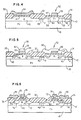
- a second photoresist mask 36 illustrated in Fig. 2, is provided over the first polysilicon layer 18 and the exposed surfaces of the silicon dioxide layer 14 having an opening 38 to define an N well 40, wherein phosphorous ions are implanted.
- a second layer of polysilicon is, preferably, directionally evaporated over the second photoresist mask 36 and into the opening 38 forming first and second polysilicon segments 42 and 44, respectively.
- This polysilicon layer may be semi-crystalline or amorphous at this point in the process.
- boron is implanted into selected portions of the surface of the P- epitaxial layer 12 defined by the pad 28 and polysilicon segment 44 for providing N channel device field regions 46 and 48, indicated in Fig. 3. All remaining polysilicon is now stripped and the semi-recessed oxide regions 30, 32 and 34 are grown adjacent to thin silicon dioxide regiokns 14' and 14" which have been protected by the silicon nitride layer 16 in pads 26 and 28. The pads 26 and 28 are then stripped, gate insulators, such as 14' and 14", are regrown and a boron channel implant is performed.
- a third layer of polysilicon is deposited over the thin silicon dioxide regions 14' and 14" and the recessed oxide regions 30, 32 and 34 and appropriately selectively etched with the use of a third photoresist mask, not shown, to form a first segment for use as a first gate electrode 50 of a first device 52 and a second segment 54 for use as an ion mask to protect the N well 40.
- Arsenic ions are implanted to form N+ source and drain regions 56 and 58 for the first device 52, followed by a heating step to partially drive in the arsenic ions.
- Any appropriate passifying layer such as phosphosilicate glass, may now be provided over the surface of the structure and appropriate contact holes defined and opened with the use of a fifth photoresist mask, not shown.
- a metal layer e.g., copper-doped aluminum, is deposited over the passifying layer and into the openings and etched so as to form contacts such as gate electrode contacts 76 and 78 for gate electrodes 50 and 66, respectively, and source/drain region contacts such as 80 and 82.
- the first definition leaves the N channel gate electrode and the P channel gate electrode and diffusion regions covered or protected by the polysilicon layer, and the second definition leaves polysilicon over only the P channel and N channel gate electrodes of transistors 52 and 68, with a photoresist mask covering the diffusion regions of transistor 52.
- the threshold of the P channel transistor is generally too negative in this structure in view of the work function of N+ polysilicon used to form the gate electrode 66.
- N channel boron channel implant the threshold is increased toward zero volts.
- the threshold may be further controlled by the use of multiple implants when forming the N well. lm- plants of different energies allow independent control of the well depth and surface doping. A deep well with a relatively low surface doping also serves to move the P channel threshold toward zero and aids in latch-up prevention by the use of the retrograde well.
- the P channel threshold is lowered while the N channel threshold is raised to provide near optimum threshold values in a CMOS structure.
Landscapes
- Metal-Oxide And Bipolar Metal-Oxide Semiconductor Integrated Circuits (AREA)
- Bipolar Transistors (AREA)
- Formation Of Insulating Films (AREA)
Claims (11)
Priority Applications (1)
| Application Number | Priority Date | Filing Date | Title |
|---|---|---|---|
| AT83110131T ATE26897T1 (de) | 1982-12-09 | 1983-10-11 | Verfahren zum herstellen komplementaerer metalloxid-halbleiterstrukturen. |
Applications Claiming Priority (2)
| Application Number | Priority Date | Filing Date | Title |
|---|---|---|---|
| US06/448,125 US4470191A (en) | 1982-12-09 | 1982-12-09 | Process for making complementary transistors by sequential implantations using oxidation barrier masking layer |
| US448125 | 1999-11-24 |
Publications (2)
| Publication Number | Publication Date |
|---|---|
| EP0111098A1 EP0111098A1 (de) | 1984-06-20 |
| EP0111098B1 true EP0111098B1 (de) | 1987-04-29 |
Family
ID=23779101
Family Applications (1)
| Application Number | Title | Priority Date | Filing Date |
|---|---|---|---|
| EP83110131A Expired EP0111098B1 (de) | 1982-12-09 | 1983-10-11 | Verfahren zum Herstellen komplementärer Metall-Oxid-Halbleiterstrukturen |
Country Status (7)
| Country | Link |
|---|---|
| US (1) | US4470191A (de) |
| EP (1) | EP0111098B1 (de) |
| JP (1) | JPS59111359A (de) |
| AT (1) | ATE26897T1 (de) |
| BR (1) | BR8306653A (de) |
| CA (1) | CA1191973A (de) |
| DE (1) | DE3371264D1 (de) |
Families Citing this family (11)
| Publication number | Priority date | Publication date | Assignee | Title |
|---|---|---|---|---|
| US4574467A (en) * | 1983-08-31 | 1986-03-11 | Solid State Scientific, Inc. | N- well CMOS process on a P substrate with double field guard rings and a PMOS buried channel |
| US4839542A (en) * | 1984-08-21 | 1989-06-13 | General Datacomm Industries, Inc. | Active transconductance filter device |
| US4600445A (en) * | 1984-09-14 | 1986-07-15 | International Business Machines Corporation | Process for making self aligned field isolation regions in a semiconductor substrate |
| US4584027A (en) * | 1984-11-07 | 1986-04-22 | Ncr Corporation | Twin well single mask CMOS process |
| US4707455A (en) * | 1986-11-26 | 1987-11-17 | General Electric Company | Method of fabricating a twin tub CMOS device |
| US5132236A (en) * | 1991-07-30 | 1992-07-21 | Micron Technology, Inc. | Method of semiconductor manufacture using an inverse self-aligned mask |
| US5233080A (en) * | 1992-09-25 | 1993-08-03 | E. I. Du Pont De Nemours And Company | Preparation of N-acylaminomethylphosphonic acids and aminomethylphosphonic acids |
| JP3958388B2 (ja) * | 1996-08-26 | 2007-08-15 | 株式会社ルネサステクノロジ | 半導体装置 |
| US5956583A (en) * | 1997-06-30 | 1999-09-21 | Fuller; Robert T. | Method for forming complementary wells and self-aligned trench with a single mask |
| US6274443B1 (en) * | 1998-09-28 | 2001-08-14 | Advanced Micro Devices, Inc. | Simplified graded LDD transistor using controlled polysilicon gate profile |
| US6063672A (en) * | 1999-02-05 | 2000-05-16 | Lsi Logic Corporation | NMOS electrostatic discharge protection device and method for CMOS integrated circuit |
Family Cites Families (16)
| Publication number | Priority date | Publication date | Assignee | Title |
|---|---|---|---|---|
| US3700507A (en) * | 1969-10-21 | 1972-10-24 | Rca Corp | Method of making complementary insulated gate field effect transistors |
| NL160988C (nl) * | 1971-06-08 | 1979-12-17 | Philips Nv | Halfgeleiderinrichting met een halfgeleiderlichaam, be- vattende ten minste een eerste veldeffecttransistor met geisoleerde stuurelektrode en werkwijze voor de vervaar- diging van de halfgeleiderinrichting. |
| US3999213A (en) * | 1972-04-14 | 1976-12-21 | U.S. Philips Corporation | Semiconductor device and method of manufacturing the device |
| US4033797A (en) * | 1973-05-21 | 1977-07-05 | Hughes Aircraft Company | Method of manufacturing a complementary metal-insulation-semiconductor circuit |
| US4027380A (en) * | 1974-06-03 | 1977-06-07 | Fairchild Camera And Instrument Corporation | Complementary insulated gate field effect transistor structure and process for fabricating the structure |
| US4002501A (en) * | 1975-06-16 | 1977-01-11 | Rockwell International Corporation | High speed, high yield CMOS/SOS process |
| US4045250A (en) * | 1975-08-04 | 1977-08-30 | Rca Corporation | Method of making a semiconductor device |
| JPS5286083A (en) * | 1976-01-12 | 1977-07-16 | Hitachi Ltd | Production of complimentary isolation gate field effect transistor |
| US4183134A (en) * | 1977-02-15 | 1980-01-15 | Westinghouse Electric Corp. | High yield processing for silicon-on-sapphire CMOS integrated circuits |
| US4224733A (en) * | 1977-10-11 | 1980-09-30 | Fujitsu Limited | Ion implantation method |
| US4244752A (en) * | 1979-03-06 | 1981-01-13 | Burroughs Corporation | Single mask method of fabricating complementary integrated circuits |
| US4306916A (en) * | 1979-09-20 | 1981-12-22 | American Microsystems, Inc. | CMOS P-Well selective implant method |
| US4382827A (en) * | 1981-04-27 | 1983-05-10 | Ncr Corporation | Silicon nitride S/D ion implant mask in CMOS device fabrication |
| US4385947A (en) * | 1981-07-29 | 1983-05-31 | Harris Corporation | Method for fabricating CMOS in P substrate with single guard ring using local oxidation |
| US4399605A (en) * | 1982-02-26 | 1983-08-23 | International Business Machines Corporation | Method of making dense complementary transistors |
| US4412375A (en) * | 1982-06-10 | 1983-11-01 | Intel Corporation | Method for fabricating CMOS devices with guardband |
-
1982
- 1982-12-09 US US06/448,125 patent/US4470191A/en not_active Expired - Lifetime
-
1983
- 1983-07-20 JP JP58131118A patent/JPS59111359A/ja active Pending
- 1983-10-11 DE DE8383110131T patent/DE3371264D1/de not_active Expired
- 1983-10-11 AT AT83110131T patent/ATE26897T1/de active
- 1983-10-11 EP EP83110131A patent/EP0111098B1/de not_active Expired
- 1983-11-08 CA CA000440689A patent/CA1191973A/en not_active Expired
- 1983-12-02 BR BR8306653A patent/BR8306653A/pt unknown
Also Published As
| Publication number | Publication date |
|---|---|
| ATE26897T1 (de) | 1987-05-15 |
| JPS59111359A (ja) | 1984-06-27 |
| BR8306653A (pt) | 1984-07-31 |
| CA1191973A (en) | 1985-08-13 |
| EP0111098A1 (de) | 1984-06-20 |
| DE3371264D1 (en) | 1987-06-04 |
| US4470191A (en) | 1984-09-11 |
Similar Documents
| Publication | Publication Date | Title |
|---|---|---|
| US4480375A (en) | Simple process for making complementary transistors | |
| US4422885A (en) | Polysilicon-doped-first CMOS process | |
| EP0067206B1 (de) | Verfahren zur herstellung komplementärer halbleiteranordnungen | |
| US4978629A (en) | Method of making a metal-oxide-semiconductor device having shallow source and drain diffused regions | |
| US4199773A (en) | Insulated gate field effect silicon-on-sapphire transistor and method of making same | |
| EP0087573B1 (de) | Verfahren zum Herstellen komplementärer Feldeffekttransistoren | |
| EP0258396B1 (de) | Herstellungsverfahren für gestapelte mos-bauelemente | |
| EP0081998A2 (de) | Verfahren zur Herstellung einer MOS Anordnung auf einem Substrat | |
| GB2090062A (en) | Igfet manufacture | |
| US5686324A (en) | Process for forming LDD CMOS using large-tilt-angle ion implantation | |
| US5422301A (en) | Method of manufacturing semiconductor device with MOSFET | |
| US4637128A (en) | Method of producing semiconductor device | |
| US4507846A (en) | Method for making complementary MOS semiconductor devices | |
| US4470191A (en) | Process for making complementary transistors by sequential implantations using oxidation barrier masking layer | |
| EP0110103B1 (de) | Verfahren zum Herstellen einer CMOS-Struktur | |
| US5225357A (en) | Low P+ contact resistance formation by double implant | |
| EP0459398A2 (de) | Herstellungsverfahren eines Kanals in MOS-Halbleiteranordnung | |
| US4471523A (en) | Self-aligned field implant for oxide-isolated CMOS FET | |
| US4517731A (en) | Double polysilicon process for fabricating CMOS integrated circuits | |
| JPH06104446A (ja) | 半導体装置 | |
| US4826783A (en) | Method for fabricating a BiCMOS device | |
| JPS6360549B2 (de) | ||
| US6316804B1 (en) | Oxygen implant self-aligned, floating gate and isolation structure | |
| US20040169224A1 (en) | Semiconductor device and manufacturing method therefor | |
| US4653173A (en) | Method of manufacturing an insulated gate field effect device |
Legal Events
| Date | Code | Title | Description |
|---|---|---|---|
| PUAI | Public reference made under article 153(3) epc to a published international application that has entered the european phase |
Free format text: ORIGINAL CODE: 0009012 |
|
| AK | Designated contracting states |
Designated state(s): AT DE FR GB IT NL |
|
| 17P | Request for examination filed |
Effective date: 19841029 |
|
| 17Q | First examination report despatched |
Effective date: 19860121 |
|
| GRAA | (expected) grant |
Free format text: ORIGINAL CODE: 0009210 |
|
| AK | Designated contracting states |
Kind code of ref document: B1 Designated state(s): AT DE FR GB IT NL |
|
| REF | Corresponds to: |
Ref document number: 26897 Country of ref document: AT Date of ref document: 19870515 Kind code of ref document: T |
|
| REF | Corresponds to: |
Ref document number: 3371264 Country of ref document: DE Date of ref document: 19870604 |
|
| ET | Fr: translation filed | ||
| ITF | It: translation for a ep patent filed | ||
| PLBE | No opposition filed within time limit |
Free format text: ORIGINAL CODE: 0009261 |
|
| STAA | Information on the status of an ep patent application or granted ep patent |
Free format text: STATUS: NO OPPOSITION FILED WITHIN TIME LIMIT |
|
| 26N | No opposition filed | ||
| ITTA | It: last paid annual fee | ||
| PGFP | Annual fee paid to national office [announced via postgrant information from national office to epo] |
Ref country code: NL Payment date: 19911031 Year of fee payment: 9 |
|
| PGFP | Annual fee paid to national office [announced via postgrant information from national office to epo] |
Ref country code: FR Payment date: 19920928 Year of fee payment: 10 |
|
| PG25 | Lapsed in a contracting state [announced via postgrant information from national office to epo] |
Ref country code: NL Effective date: 19930501 |
|
| NLV4 | Nl: lapsed or anulled due to non-payment of the annual fee | ||
| PG25 | Lapsed in a contracting state [announced via postgrant information from national office to epo] |
Ref country code: FR Effective date: 19940630 |
|
| REG | Reference to a national code |
Ref country code: FR Ref legal event code: ST |
|
| PGFP | Annual fee paid to national office [announced via postgrant information from national office to epo] |
Ref country code: AT Payment date: 19950825 Year of fee payment: 13 |
|
| PGFP | Annual fee paid to national office [announced via postgrant information from national office to epo] |
Ref country code: DE Payment date: 19951030 Year of fee payment: 13 |
|
| PGFP | Annual fee paid to national office [announced via postgrant information from national office to epo] |
Ref country code: GB Payment date: 19960925 Year of fee payment: 14 |
|
| PG25 | Lapsed in a contracting state [announced via postgrant information from national office to epo] |
Ref country code: AT Effective date: 19961011 |
|
| PG25 | Lapsed in a contracting state [announced via postgrant information from national office to epo] |
Ref country code: DE Effective date: 19970701 |
|
| PG25 | Lapsed in a contracting state [announced via postgrant information from national office to epo] |
Ref country code: GB Free format text: LAPSE BECAUSE OF NON-PAYMENT OF DUE FEES Effective date: 19971011 |
|
| GBPC | Gb: european patent ceased through non-payment of renewal fee |
Effective date: 19971011 |