EP0111406B1 - Arrangement et méthode pour garantir l'intégrité d'une transmission - Google Patents
Arrangement et méthode pour garantir l'intégrité d'une transmission Download PDFInfo
- Publication number
- EP0111406B1 EP0111406B1 EP83307310A EP83307310A EP0111406B1 EP 0111406 B1 EP0111406 B1 EP 0111406B1 EP 83307310 A EP83307310 A EP 83307310A EP 83307310 A EP83307310 A EP 83307310A EP 0111406 B1 EP0111406 B1 EP 0111406B1
- Authority
- EP
- European Patent Office
- Prior art keywords
- parity
- data
- channel
- transmission
- word
- Prior art date
- Legal status (The legal status is an assumption and is not a legal conclusion. Google has not performed a legal analysis and makes no representation as to the accuracy of the status listed.)
- Expired
Links
Images


Classifications
-
- H—ELECTRICITY
- H04—ELECTRIC COMMUNICATION TECHNIQUE
- H04Q—SELECTING
- H04Q11/00—Selecting arrangements for multiplex systems
- H04Q11/04—Selecting arrangements for multiplex systems for time-division multiplexing
-
- G—PHYSICS
- G06—COMPUTING OR CALCULATING; COUNTING
- G06F—ELECTRIC DIGITAL DATA PROCESSING
- G06F11/00—Error detection; Error correction; Monitoring
- G06F11/07—Responding to the occurrence of a fault, e.g. fault tolerance
- G06F11/08—Error detection or correction by redundancy in data representation, e.g. by using checking codes
- G06F11/10—Adding special bits or symbols to the coded information, e.g. parity check, casting out 9's or 11's
-
- H—ELECTRICITY
- H04—ELECTRIC COMMUNICATION TECHNIQUE
- H04M—TELEPHONIC COMMUNICATION
- H04M3/00—Automatic or semi-automatic exchanges
- H04M3/22—Arrangements for supervision, monitoring or testing
- H04M3/24—Arrangements for supervision, monitoring or testing with provision for checking the normal operation
- H04M3/244—Arrangements for supervision, monitoring or testing with provision for checking the normal operation for multiplex systems
Definitions
- This invention relates generally to digital transmission e.g. between a central host telephone switching office and one or more remote offices.
- One digital time division telephone electronic switching system utilizing stored program control broadly has a central processor (CP), a message switch (MSGS), a time-multiplexed switch (TMS) and one or more interface modules (IM).
- the central processor provides central control of all switching functions as well as memory, bulk storage and data link interfaces.
- the message switch provides duplicated control and message data transfer between the central processor at a Host Office and the interface modules.
- the Time multiplexed switch is a time-shared space division switch providing routing paths for control and data messages in pulse-code modulation (PCM) format among the interface modules.
- PCM pulse-code modulation
- the interface modules terminate telephone subscriber lines and trunks from other telephone central offices. Analog signals are converted into the PCM format within the interface modules.
- a time-slot interchange (TSI) unit within each interface module performs time-division switching while the time multiplexed switch performs space division switching.
- the signalling and data paths between interface modules and the time multiplexed switch are affected through four network, control and timing (NCT) links, (two of which are active) and may be implemented using fiber optic technology.
- Network, control and timing link provides 256 time slots (TS), each of which contains sixteen bits sampled at a baud rate of 8000.
- a frame of 256 TS with 16 bits per TS has a length of 4,096 bits and the overall high-speed data rate therefore becomes 32.768 million bits per second (Mb/s).
- T1 lines for example the facilities known by the Bell System designation T1 lines.
- up to ten T1 lines, each providing twenty-four eight-bit PCM channels, are mapped into each of the active network control and timing links at the maximum capacity of ten T1 lines per link.
- 230 of the 256 available time lots in each network control and timing link are available for message traffic and control data.
- the integrity of the several components in the transmission facilities between the host and remote interface modules can be tested continuously and the location and type of error arising assessed.
- a fixed alternation of parity is assigned to successive transmission channels in one direction of transmission and the same parity is repeated on successive transmission channels in the opposite direction of transmission at the interface between T1 lines and the network, control and timing links.
- This pattern of parity is repeated every two frames.
- the pattern sent in the even-numbered frame is the inverse of that in the odd-numbered frame.
- the invention provides a transmission integrity arrangement for a two way plural-channel communication system having first and second preprogrammed memories for opposite transmission directions which store a line of data for each channel in said system including selection sequence codes for all channels and parity bits for the originating channel, the sequence code and the overall data line; a counter arranged to control the read-out of lines of data from said memories in sequence; a parity generator responsive to said second preprogrammed memory to compute the parity on each data channel for one transmission direction; a parity checker responsive to said first preprogrammed memory to examine the parity on each data channel for the opposite transmission direction; and an error register to record each parity failure and generate an interrupt signal.
- a remote switching module in an electronic telephone switching system is placed under the control of a central processor (CP) at a host office through plurality of pulse-code-modulation (PCM) digital transmission channels provided over a plurality of T1 carrier lines and terminating in a digital facilities interface (DFI) at a facilities interface unit (FIU) which remaps the parallel T1 carrier links into two redundant pairs of high-speed serial streams of network, control and timing (NCT) link signals.
- One pair is normally in active service, while the other is in backup or standby service.
- a structured pattern of alternate odd and even parity is interactively applied to data words in the several peripheral interface data buses (PIDB) interconnecting the DFis and the FIU for both transmission directions such that the parity in a particular bus in one transmission direction is repeated in the same signalling channel in the return transmission direction.
- PIDB peripheral interface data buses
- the parity pattern for each direction of transmission is predetermined and stored in read-only memories (ROM) according to the addresses of the time slots.
- ROM read-only memories
- the PCM channels in up to ten T1 links are combined in a multiplexer-demultiplexer (MUX) circuit (two redundant pairs of which are normally provided, one pair in active service and one on standby).
- MUX multiplexer-demultiplexer
- redundant pairs of serial data streams are formed on the NCT links from thirty-two time slots PIDBs with a sixteen-bit word, in each time slot into frames containing 256 time slots.
- the 24 PCM words per frame on each T1 link are formatted by the DFI into the 32 time slots of the serial streams on the PIDBs, by stuffing every fourth time slot with a prearranged idle code.
- the stuffed time slots are staggered for more uniform distribution throughout the serial data streams.
- the transmit ROM stores select code and assigned parity information by PIDB address for data moving from the serial stream in the NCT link to the DFI.
- a receive ROM stores select code, and parity information by PIDB address for data moving in the opposite direction.
- a single counter synchronizes the reading of each ROM with the data words being transmitted.
- Each ROM contains a data word of sufficient length, say, eight bits, to identify the proper PIDB and DFI, the assigned parity sense of that word, the parity of the address of the time slot and the overall parity of the data word read from the ROM.
- a parity circuit is further provided for each direction of transmission to generate the assigned parities on the transmit side and to check the received parity on the receive side.
- a continuous maintenance test is performed which can detect single hardware faults by using the patterned parity scheme recorded in the ROMs.
- Each DFI detects parity over the incoming time slots in the serial data stream from the NCT links.
- the detected parity sequence is then applied to the next frame of data that is to be returned to the serial stream from the associated DFI.
- the parity sequence of the next returned frame of data is checked against that of the previous transmitted parity by the MUX.
- an error register records the error occurrence and reports it to the MP.
- Two types of l o opback between transmit and receive transmission directions are provided to help isolate faults to a portion of the FIU or the DFI.
- Data can be looped back through the link interfaces to isolate parity failures to the FIU hardware or to the NCT link.
- a peripheral loopback can be effected across the DFI side of the FIU to isolate faults to the MUX or to the DFIs and their buses.
- the FIU multiplexer-demultiplexer arrangement of this invention comprises a continuous parity checking scheme for preserving the integrity of data traversing the arrangement.
- Fig. 1 is a simplified block diagram of a digital time division telephone switching system to which the data integrity control arrangement of this invention is applicable.
- the system is designed in a modular architecture with a view to ready expansion over a wide range of subscriber loading.
- the host office comprises central processor (CP) 100, message switch (MSGS) 101, time multiplex switch (TMS) 102 and one or more interface modules (IM), such as those designated 103 and 107.
- CP central processor
- MSGS message switch
- TMS time multiplex switch
- IM interface modules
- Local subscriber sets 104 and 105 are shown connected to IM 103.
- Stub 106 represents a network, control and timing link (NCT) to a further interface module (not shown).
- IM 107 provides connections through T1 carrier links 108 to a remote office.
- Each bidirectional T1 carrier link 108 interfaces with IM 107 through an individual digital facilities interface (DFI) 115, as shown.
- DFI digital facilities interface
- the remote office further comprises facilities interface unit (FIU) 109, serial network control and timing (NCT) links 110, remote module (RM) 111 and module processor (MP) 112.
- FIU 109 terminates T1 carrier links 108 through individual matching DFls 116, as shown. Subscriber sets 113 and 114 are shown terminated at RM 111.
- CP 100 implements a portion of the stored program aspect of the overall switching system by providing for central control, memory, bulk storage and data link interface functions. Through a combination of hardware and software operating and maintenance functions, including error and fault detection and diagnostic routines, calls are monitored and controlled.
- MSGS 101 provides control message transfer between CP 100 and the IMs, such as those designated 103 and 107.
- Control messages convey information on which routes to select, what service to provide and the like. These messages are passed over high speed NCT digital links through the TMS to an IM.
- TMS 102 is a time-shared, space division switch that interconnects the seveal IMs that may be located in the same central office, including the IM (107) that is connected to a remote office. Control, data and PCM encoded voice signals are routed among the IMs by the TMS.
- Each IM includes a time slot interchanger (TSI) for establishing paths between time slots in the NCT digital links and the time slots assigned to the lines terminating in the IMs.
- IMs convert signals received from analog lines and trunks into a digital, time-division format. Where only one IM is placed in a host office, the TMS is superfluous.
- Setting up a path between a line or trunk terminating on one IM and a line or trunk terminating on another IM involves finding a common time slot on one of the NCT serial links to each IM. A path is then set up through TMS -102 between the two NCT links during that time slot. Then, the TSI within each IM establishes a further path between the chosen serial link time slot and the peripheral time slot corresponding to the respective line or trunk.
- RM 111 is similar to IM 103 in that it provides termations for subscriber sets, such as those designated 113 and 114.
- Two NCT serial links 110 provide bidirectional serial time slots to and from the host office.
- RM 111 has associated with it its own MP 112 which enables it to stand alone in providing service to subscribers that are terminated directly should the link to the CP at the host office be severed. Connections between the host office and RM 111 are provided over T1 carrier links 108.
- FIU 109 interposed between T1 links 108 and NCT links 110, terminates T1 links 108 and formats data and control signals on these links into NCT links 110.
- Fig. 2 is a more detailed block diagram of a portion of T1 links 108 and FIU 109.
- FIU 109 contains a multiplexer-demultiplexer (MUX) arrangement for the transmission facilities between the host office and a remote switching module.
- MUX multiplexer-demultiplexer
- twenty-four digital channels of information are interchanged in time-division multiplex fashion over each of a plurality of parallel links commonly called T1 carrier lines.
- One of these twenty-four channels carries control signals.
- the other channels carry customer messages, such as, data or coded speech.
- the T1 digital format includes 24 time-divided 8-bit channels.
- the data format to FIU 109 provides, on the other hand, 32 time-divided 16-bit channels.
- the extra bits in the FIU channels are provided to include parity, busy/idle status and other signalling information.
- NCT links 110 are of still another format. Each link contains in each direction 256 separate 16-bit time slots at a baud rate of 8000. As shown in Fig. 5, each serial link time slot uses 8 bits BO through B7 to carry a PCM word, 4 bits A through D for control signalling, bit E for time slot activity status, bits F and G for internal control and bit P for odd parity across the time slot. With the 8000 Hz sampling rate, 256 time operating and 16 bits per time slot, the frame length becomes 4096 bits. The overall data rate is thus 32.768 megabits per second.
- the FIU of Fig. 2 interfaces with a telephone trunk facility comprising a plurality ofT1 links 108 on the host office side terminated in individual digital facilities interface (DFI) units.
- DF is recover data, control and timing information.
- Special messages sent over a derived data link contained in the special framing of each T1 link can be decoded for the purpose of establishing communication on the start up of the system beween the CP at the host office and the MP at the remote office. All FIU functions are performed by redundant hardware (not shown) to increase reliability and to serve as a ready back-up to the active hardware.
- a plurality of T1 links 108 terminate through lines, such as those designated 201 and 202, in a plurality of DFIs (from 4 to 20) such as those designated 203 and 204.
- DFls 203 and 204 are controlled through signals from MP 112 over peripheral control channels (not shown).
- 23 clear data channels and one signaling channel are provided on each T1 link.
- a local oscillator in each DFI is synchronized with a 1.544 MHz clock signal recovered from the host office data stream.
- the several DFis are connected over peripheral interface data buses (PIDB) 206 to peripheral receiver 209 and peripheral transmitter 212.
- Bus 205 is the receive side of a specific one of buses 206 joining DFI 203 to peripheral receiver 209.
- Bus 208 is the transmit side of a specific one of buses 206 joining DFI 204 to peripheral transmitter 212.
- the remaining DFis similarly have their transmit and receive ports connected to receiver 209 and transmitter 221. Signals outgoing from the host office on the several T1 links 108 are reformatted into the 256 time slot NCT data format in peripheral receiver 209. Signals incoming from the remote office on the NCT link are time divided among the several DFis in peripheral transmitter 212.
- Peripheral receiver 209 and peripheral transmitter 212 together constitute a multiplexer-demultiplexer arrangement (MUX) in the FIU.
- MUX multiplexer-demultiplexer arrangement
- the 24 eight-bit words of a frame on each T1 link are transformed into 256 NCT time slots of sixteen bits each for use in serial links 110. Since there are 32 time slots in a frame of the PIDB bus to carry the 24 channels of each PCM frame there are eight excess time slots in each frame.
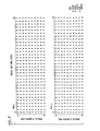
- Fig. 3 is an assignment diagram showing an orderly distribution of 24 channels of ten PCM links among successive 32-time slot frames of the serial link.
- the letter "s" in the several positions indicates the assignment of a stuffing idle-code word of sixteen-bit length of the form 0111111100001111.
- the eight-bit PCM words are extended to sixteen bits as previously mentioned in connection with Fig. 5.
- the P bit places assigned parity across the time slot. It is apparent that the stuffed idle codes recur in a recognizable sequence.
- With ten T1 links each with 24 channels per frame 240 of the 256 serial time slots in a frame are assigned, only 230 of which are available for call data. The remaining sixteen time slots are not supplied with data by the host office. Where fewer than ten T1 links are in service, idle code is inserted by the MUX into the unassigned data words, including the sixteen excess time slots.
- the transition from T1 carrier links 108 to NCT links 110 is effected in the FIU through a multiplexer-demultiplexer arrangement comprising DFis 203 and 204, peripheral transmitter 212, peripheral receiver 209, peripheral loopback 210, receive read only memory (ROM) 213, transmit ROM 216, clock counter 214, receive parity generator 217, transmit parity generator 220, error register 218, link interfaces (LI) 221 and 224 and link loopback 222.
- ROM read only memory
- ROM read only memory
- clock counter 214 receive parity generator 217
- transmit parity generator 220 transmit parity generator 220
- error register 218 link interfaces (LI) 221 and 224 and link loopback 222.
- Data to be sent from NCT links 110 toward the host office connected to T1 links 108 are transmitted by LI 224 in 4 bit nibbles at an approximate eight MHz rate. There are sixteen bits in each data word as shown in Fig. 5. Each word is divided into four nibbles B7 through B4, B3 through BO A through D and E through P. Nibbles are carried over four wire buses. The overall word rate is thus 2 MHz. Within the transmit portion of the arrangement, data are maintained in this nibble format to facilitate the provision of frame synchronization, a fixed parity test and loopback testing.
- Each multiplexer interfaces with its group of DFis over PIDBs.
- Each PIDB transmits 32 time slots of 16 bit serial data over twisted wire pairs to and from the DFI during each serial frame.
- a 4 MHz bit clock and an 8 MHz sync pulse are also provided.
- the value of the parity bit in each 16-bit word is determined by a fixed algorithm of patterned parity indicated further in Fig. 3. Even parity is inserted into three time slots of each PIDB serial frame as shown, for example, in the 0, 10 and 20 time slot positions of the top line of Fig. 3. In the next line even parity is assigned to the 1, 11 and 21 time slot positions. This pattern is continued through the remaining lines. All the remaining time slots in active use (those not stuffed with idle code) carry odd parity.
- the odd and even parity assignments are reversed.
- the assigned parity is a function both of the time slot position and the DFI address (0 to 9).
- the parity sequence on each PIDB is unique. Since a DFI is arranged to echo the assigned parity scheme on its next frame of data sent back to the MUX, the MUX is able to test each PIDB, a portion of each DFI and its own parity generator.
- the source of the receive data and the d estin- ation of the transmit data are stored in ROMs 213 and 216, respectively. These ROMs, addressed in sequence by the time slot count value, produce a selection code, the parity value expected to be received or sent in that time slot and a bit which forces the ROM data word parity to be odd for a self check, as shown in Fig. 4.
- Signals directed from host office to the remote module are passed from peripheral receiver 209 to receive parity 217 over path 227.
- Receive ROM 213 provides the assigned parity for comparison purposes.
- Signals directed from the remote module toward the host office are passed from transmit parity 220 to peripheral transmitter 212 over path 228.
- Transmit ROM 216 provides the assigned parity for comparison purposes.
- the resultant ROM data are stored for use in the following time slot.
- This delay in the use of ROM data lends itself to an address bus checking scheme.
- the receive ROM stores a parity bit which, when compared with the parity of the present address bit signals in an exclusive-OR gate arrangement, must produce odd parity.
- the data word output for each ROM is tested for odd parity every time slot.
- a stuck clock counter bit can be detected once every frame. If an error is detected on the receive ROM data bus or on the ROM address bus, the receive ROM bit is set to one in error register 218. Similarly, when a transmit ROM parity error occurs, the transmit ROM bit is set to one in error register 218.
- All timing signals in the MUX are synchronized to time slot clock-counter 214 by 16 and 8 MHz clock signals and a negative-going sync pulse that occurs on alternate NCT link frames for the duration of an 8 MHz clock cycle.
- a continuous maintenance test is performed in the MUX by means of the patterned parity scheme.
- the proper parity sequence is forced on the transmitted data stream by transmit parity generator 220.
- Each DFI detects this parity sequence over the 32 time slots on PIDB 208 from peripheral transmitter 212.
- This parity is used to format the parity of the next frame of data returned to the MUX by way of peripheral receiver 209.
- the parity received is then checked against that stored in receive ROM 213 by receive parity checker 217. If the two patterns differ, an error-source register bit in error register 218 is set and an interrupt signal is sent to the MP. The MP then initiates a diagnostic procedure to isolate the failure.
- the MUX can perform two types of data loopback on demand to isolate troubles within the interface hardware of Fig. 2.
- One loopback occurs in block 222 between incoming and outgoing link interfaces 224 and 221.
- a second loopback occurs in block 210 between the incoming and outgoing buses 206 to a particular DFI by way of peripheral transmitter 212 and peripheral receiver 209.
- a time slot count is derived from the system clock by way of clock counter 214. This count is applied to the address bus of each ROM 213 and 216.
- the data access time of each ROM is only slightly less than the duration of a time slot. Therefore, ROM data is latched in a flip-flop type register, and used during the succeeding time slot.
- the ROM data bit definition for each time slot bus is shown in Fig. 4, as prevously discussed.
Landscapes
- Engineering & Computer Science (AREA)
- Computer Networks & Wireless Communication (AREA)
- Signal Processing (AREA)
- Theoretical Computer Science (AREA)
- Quality & Reliability (AREA)
- Physics & Mathematics (AREA)
- General Engineering & Computer Science (AREA)
- General Physics & Mathematics (AREA)
- Use Of Switch Circuits For Exchanges And Methods Of Control Of Multiplex Exchanges (AREA)
- Time-Division Multiplex Systems (AREA)
- Monitoring And Testing Of Exchanges (AREA)
- Exchange Systems With Centralized Control (AREA)
Claims (5)
Applications Claiming Priority (2)
| Application Number | Priority Date | Filing Date | Title |
|---|---|---|---|
| US06/447,008 US4546475A (en) | 1982-12-06 | 1982-12-06 | Parity checking arrangement |
| US447008 | 1982-12-06 |
Publications (2)
| Publication Number | Publication Date |
|---|---|
| EP0111406A1 EP0111406A1 (fr) | 1984-06-20 |
| EP0111406B1 true EP0111406B1 (fr) | 1986-04-30 |
Family
ID=23774641
Family Applications (1)
| Application Number | Title | Priority Date | Filing Date |
|---|---|---|---|
| EP83307310A Expired EP0111406B1 (fr) | 1982-12-06 | 1983-12-01 | Arrangement et méthode pour garantir l'intégrité d'une transmission |
Country Status (8)
| Country | Link |
|---|---|
| US (1) | US4546475A (fr) |
| EP (1) | EP0111406B1 (fr) |
| JP (1) | JPS59112792A (fr) |
| KR (1) | KR920003264B1 (fr) |
| AU (1) | AU539842B2 (fr) |
| CA (1) | CA1203025A (fr) |
| DE (1) | DE3363300D1 (fr) |
| GB (1) | GB2131653B (fr) |
Families Citing this family (12)
| Publication number | Priority date | Publication date | Assignee | Title |
|---|---|---|---|---|
| US4592044A (en) * | 1984-05-22 | 1986-05-27 | At&T Information Systems Inc. | Apparatus and method for checking time slot integrity of a switching system |
| EP0220019A3 (fr) * | 1985-10-17 | 1989-10-25 | AT&T Corp. | Procédé de commande d'un banc de canaux D-5 et dispositif de commande |
| FR2642590B1 (fr) * | 1989-02-02 | 1995-01-13 | Cit Alcatel | |
| ATE125386T1 (de) * | 1989-05-31 | 1995-08-15 | Siemens Ag | Verfahren und vorrichtung zum internen paralleltest von halbleiterspeichern. |
| EP0485025A1 (fr) * | 1990-11-09 | 1992-05-13 | Trt Telecommunications Radioelectriques Et Telephoniques | Système de transmission de données comportant une pluralité de circuits satellites sur une ligne de données |
| US5416772A (en) * | 1993-08-20 | 1995-05-16 | At&T Corp. | Apparatus for insertion of overhead protocol data into a switched data stream |
| US5838698A (en) * | 1995-04-28 | 1998-11-17 | Lucent Technologies Inc. | Alignment of parity bits to eliminate errors in switching from an active to a standby processing circuit |
| SE505322C2 (sv) * | 1995-12-29 | 1997-08-04 | Ericsson Telefon Ab L M | Rutinkontroll av paritetsunderhåll |
| US5856989A (en) * | 1996-08-13 | 1999-01-05 | Hewlett-Packard Company | Method and apparatus for parity block generation |
| US6505321B1 (en) * | 1999-05-20 | 2003-01-07 | Emc Corporation | Fault tolerant parity generation |
| CN113806243B (zh) * | 2015-03-11 | 2025-05-30 | 拉姆伯斯公司 | 高性能非易失性存储器模块 |
| CN109815038B (zh) * | 2018-12-04 | 2022-03-29 | 天津大学 | 一种基于局部重布局的奇偶校验故障注入检测方法 |
Family Cites Families (5)
| Publication number | Priority date | Publication date | Assignee | Title |
|---|---|---|---|---|
| US4224681A (en) * | 1978-12-15 | 1980-09-23 | Digital Equipment Corporation | Parity processing in arithmetic operations |
| US4280217A (en) * | 1979-12-26 | 1981-07-21 | Bell Telephone Laboratories, Incorporated | Time division switching system control arrangement |
| US4296492A (en) * | 1979-12-26 | 1981-10-20 | Bell Telephone Laboratories, Incorporated | Continuity verification arrangement |
| US4346474A (en) * | 1980-07-03 | 1982-08-24 | International Business Machines Corporation | Even-odd parity checking for synchronous data transmission |
| US4429391A (en) * | 1981-05-04 | 1984-01-31 | Bell Telephone Laboratories, Incorporated | Fault and error detection arrangement |
-
1982
- 1982-12-06 US US06/447,008 patent/US4546475A/en not_active Expired - Lifetime
-
1983
- 1983-10-31 CA CA000440094A patent/CA1203025A/fr not_active Expired
- 1983-11-17 AU AU21455/83A patent/AU539842B2/en not_active Ceased
- 1983-12-01 DE DE8383307310T patent/DE3363300D1/de not_active Expired
- 1983-12-01 EP EP83307310A patent/EP0111406B1/fr not_active Expired
- 1983-12-01 GB GB08332131A patent/GB2131653B/en not_active Expired
- 1983-12-05 KR KR1019830005744A patent/KR920003264B1/ko not_active Expired
- 1983-12-06 JP JP58229260A patent/JPS59112792A/ja active Pending
Also Published As
| Publication number | Publication date |
|---|---|
| GB8332131D0 (en) | 1984-01-11 |
| DE3363300D1 (en) | 1986-06-05 |
| GB2131653B (en) | 1986-01-02 |
| JPS59112792A (ja) | 1984-06-29 |
| GB2131653A (en) | 1984-06-20 |
| CA1203025A (fr) | 1986-04-08 |
| EP0111406A1 (fr) | 1984-06-20 |
| AU539842B2 (en) | 1984-10-18 |
| KR840007499A (ko) | 1984-12-07 |
| KR920003264B1 (ko) | 1992-04-25 |
| US4546475A (en) | 1985-10-08 |
| AU2145583A (en) | 1984-06-14 |
Similar Documents
| Publication | Publication Date | Title |
|---|---|---|
| CA1260588A (fr) | Methode et dispositif pour etablir une installation de communication a large bande via un reseau de communication a canaux a bande passante etroite | |
| US4382294A (en) | Telephone switching control arrangement | |
| US4149038A (en) | Method and apparatus for fault detection in PCM muliplexed system | |
| US4494231A (en) | Time division switching system for circuit mode and packet mode channels | |
| EP0111406B1 (fr) | Arrangement et méthode pour garantir l'intégrité d'une transmission | |
| US4885738A (en) | Method of and apparatus for establishing a wideband communication facility through a switched communications network having narrow bandwidth time division multiplexed channels | |
| US4081611A (en) | Coupling network for time-division telecommunication system | |
| US6226261B1 (en) | Redundant switching arrangement | |
| US4543651A (en) | Duplicated time division switching system | |
| JPS598120B2 (ja) | デイジタルスイツチング装置 | |
| US5828664A (en) | Integrated network switch having mixed mode switching with selectable full frame/half frame switching | |
| US4254496A (en) | Digital communication bus system | |
| US4022979A (en) | Automatic in-service digital trunk checking circuit and method | |
| EP0114822B1 (fr) | Agencements de communication pour systemes repartis de commande | |
| CA1215472A (fr) | Dispositif de prise en charge du protocole pour systeme de communication multicanal | |
| US4466095A (en) | Speech path control system | |
| US4873682A (en) | Digital key telephone system | |
| JPS5821460B2 (ja) | 電話回線上で、電話信号とビデオ信号とを共に伝送するための装置 | |
| CA2151293C (fr) | Commutateur de reseau a fonctions variables | |
| US4412322A (en) | Time division switching system | |
| US4905228A (en) | Digital transmission channel framing | |
| US5610928A (en) | Data verification method | |
| US4924459A (en) | Digital transmission interconnect signal | |
| JP3004130B2 (ja) | メッセージ情報終端方式 | |
| CA1114933A (fr) | Systeme de bus de communication numerique |
Legal Events
| Date | Code | Title | Description |
|---|---|---|---|
| PUAI | Public reference made under article 153(3) epc to a published international application that has entered the european phase |
Free format text: ORIGINAL CODE: 0009012 |
|
| AK | Designated contracting states |
Designated state(s): BE DE FR NL SE |
|
| 17P | Request for examination filed |
Effective date: 19841122 |
|
| GRAA | (expected) grant |
Free format text: ORIGINAL CODE: 0009210 |
|
| AK | Designated contracting states |
Kind code of ref document: B1 Designated state(s): BE DE FR NL SE |
|
| REF | Corresponds to: |
Ref document number: 3363300 Country of ref document: DE Date of ref document: 19860605 |
|
| ET | Fr: translation filed | ||
| PLBE | No opposition filed within time limit |
Free format text: ORIGINAL CODE: 0009261 |
|
| STAA | Information on the status of an ep patent application or granted ep patent |
Free format text: STATUS: NO OPPOSITION FILED WITHIN TIME LIMIT |
|
| 26N | No opposition filed | ||
| EAL | Se: european patent in force in sweden |
Ref document number: 83307310.9 |
|
| PGFP | Annual fee paid to national office [announced via postgrant information from national office to epo] |
Ref country code: SE Payment date: 20011002 Year of fee payment: 19 |
|
| PGFP | Annual fee paid to national office [announced via postgrant information from national office to epo] |
Ref country code: BE Payment date: 20011010 Year of fee payment: 19 |
|
| PGFP | Annual fee paid to national office [announced via postgrant information from national office to epo] |
Ref country code: FR Payment date: 20011121 Year of fee payment: 19 |
|
| PGFP | Annual fee paid to national office [announced via postgrant information from national office to epo] |
Ref country code: NL Payment date: 20011127 Year of fee payment: 19 |
|
| PGFP | Annual fee paid to national office [announced via postgrant information from national office to epo] |
Ref country code: DE Payment date: 20011230 Year of fee payment: 19 |
|
| PG25 | Lapsed in a contracting state [announced via postgrant information from national office to epo] |
Ref country code: SE Free format text: LAPSE BECAUSE OF NON-PAYMENT OF DUE FEES Effective date: 20021202 |
|
| PG25 | Lapsed in a contracting state [announced via postgrant information from national office to epo] |
Ref country code: BE Free format text: LAPSE BECAUSE OF NON-PAYMENT OF DUE FEES Effective date: 20021231 |
|
| BERE | Be: lapsed |
Owner name: *WESTERN ELECTRIC CY INC. Effective date: 20021231 |
|
| PG25 | Lapsed in a contracting state [announced via postgrant information from national office to epo] |
Ref country code: NL Free format text: LAPSE BECAUSE OF NON-PAYMENT OF DUE FEES Effective date: 20030701 Ref country code: DE Free format text: LAPSE BECAUSE OF NON-PAYMENT OF DUE FEES Effective date: 20030701 |
|
| EUG | Se: european patent has lapsed | ||
| NLV4 | Nl: lapsed or anulled due to non-payment of the annual fee |
Effective date: 20030701 |
|
| PG25 | Lapsed in a contracting state [announced via postgrant information from national office to epo] |
Ref country code: FR Free format text: LAPSE BECAUSE OF NON-PAYMENT OF DUE FEES Effective date: 20030901 |
|
| REG | Reference to a national code |
Ref country code: FR Ref legal event code: ST |