EP0111879A2 - Couche à redéfinition de fonctions sensible au toucher - Google Patents
Couche à redéfinition de fonctions sensible au toucher Download PDFInfo
- Publication number
- EP0111879A2 EP0111879A2 EP83112539A EP83112539A EP0111879A2 EP 0111879 A2 EP0111879 A2 EP 0111879A2 EP 83112539 A EP83112539 A EP 83112539A EP 83112539 A EP83112539 A EP 83112539A EP 0111879 A2 EP0111879 A2 EP 0111879A2
- Authority
- EP
- European Patent Office
- Prior art keywords
- touch
- overlay
- cell
- display
- sensitive overlay
- Prior art date
- Legal status (The legal status is an assumption and is not a legal conclusion. Google has not performed a legal analysis and makes no representation as to the accuracy of the status listed.)
- Withdrawn
Links
Images

Classifications
-
- G—PHYSICS
- G06—COMPUTING OR CALCULATING; COUNTING
- G06F—ELECTRIC DIGITAL DATA PROCESSING
- G06F3/00—Input arrangements for transferring data to be processed into a form capable of being handled by the computer; Output arrangements for transferring data from processing unit to output unit, e.g. interface arrangements
- G06F3/01—Input arrangements or combined input and output arrangements for interaction between user and computer
- G06F3/03—Arrangements for converting the position or the displacement of a member into a coded form
- G06F3/041—Digitisers, e.g. for touch screens or touch pads, characterised by the transducing means
- G06F3/042—Digitisers, e.g. for touch screens or touch pads, characterised by the transducing means by opto-electronic means
- G06F3/0421—Digitisers, e.g. for touch screens or touch pads, characterised by the transducing means by opto-electronic means by interrupting or reflecting a light beam, e.g. optical touch-screen
Definitions
- the present invention relates, generally, to a touch-sensitive overlay for operator interaction with a visual or graphic display of a host system. such as a computer and, more especially, to an overlay which permits the localized identification of a position on the display upon a manual touch thereat by the operator.
- the touch-sensitive overlay of the present invention is adapted for association with any visual display where a plurality of character locations thereon are position-multiplexed within a coordinate array to define or otherwise discriminate one position from another.
- the instant overlay is capable of advantageous implementation in association with a CRT display where the raster scan is useful in providing a temporal base for character location identification, a time-multiplexed array of light-emitting devices where the multiplexing circuitry provides temporal identification for one location vis-a-vis another, or other similar display devices.
- Such direct interactive devices admit of many advantages over inputing data via, e.g., a keyboard.
- Many individuals are timid in "communicating" with a computer and this apprehension oftentimes contributes to error where information is introduced through a keyboard.
- the problem is exacerbated since the common tendency is to focus on the keys rather than on the visual display associated with the keyboard with consequent typographical errors; in turn reinforcing the psychological problem of interaction by the operator.
- Even single-function keys have not entirely overcome these problems and, in further point of fact, there is a practical limit to the ability of a manufacturer to provide a keyboard with a range of single-function keys coextensive with the contemplated uses of the system.
- a light pen for direct operator -interaction with a com puter terminal through a visual display was implemented in the form of a light pen.
- this class of device is represented by a photodetector housed within an elongate member in the shape of a conventional pen.
- the light pen is manipulated by placing the photocell in proximate contact with the face of a CRT .display at a desired location.
- the raster scans the face of the CRT it causes illumination sufficient to trigger the photocell in the pen, the physical location thereof being correlated to the raster position at the time a pulse is detected.
- a switch is included on the pen to enable the device when it is put in use; in order to avoid spurious signals.
- Light beam arrays interrupted by the presence of a finger of the operator or other intrusive object have -been proposed was a means for operator interaction with a host system.
- these devices are implemented as horizontal and vertical arrays of light emitting diodes or the like and associated detectors disposed about the periphery of, e.g., a CRT display.
- the interposition of either an operator's finger or another opaque object interrupts a given light beam, the detection of which allows the characterization of the location of the interposed object.
- the light beams are columnated in order to provide physical discrimination of points within an X-Y gridwork.
- the LED's are cycled "on” and “off” in a specific sequence so that at any given moment only appropriate ones of the emitter/detector pairs are energized in order to avoid the cost of beam columnation while nonetheless providing spatial discrimination.
- Still other approaches within this realm of optical touch panels include the use of a continuous light source with charge-couple devices (“CCD”) configured as linear image sensors. These types of panels require a continuous light source about three sides of the display with two CCD linear image detectors mounted in the corners connecting the remaining side. The CCD's are mounted at angles whereby shadows caused through interposition of an object within the light field over the display will be received by both.
- CCD charge-couple devices
- a focusing device screens shadows from the CCD's except those from which precise touch locations may be determined by appropriately referenced trigonometric equations.
- each of these approaches suffers one or more significant disadvantages.
- Each is (to-varying degrees) particu- - larly susceptible to intrusion'from ambient lighting, and particularly the continuously illuminated panel last-mentioned above.
- Columnating a matrixed array of LED's is a fairly costly approach. While that is minimized to a certain extent by sequencing the emitter/detector pairs, the curvature of a conventional CRT display poses some significant problems in initial alignment and subsequent detection irrespective of the format of emitters and detectors. Then too, such an array may oftentimes require considerable hard-wiring to provide input/ output function for the components constituting that array.
- Capacitive touch panels are also known, and typically rely upon a glass panel with conductive surfaces screened on both front and back. In this way the glass intermediate the conductive surfaces serves as the dielectric.
- the touch-sensitive capacitance switch usually consists of two such capacitors in series which have identical capacitance values correlated to an engineering design for the average capacitance of human touch at about 50 picofarads.
- a low-level signal is continuously pulsed through this switch array; which signal is shunted to ground through the body capacitance when a finger ' touches the top plate of the switch. Spatial discrimination can be achieved by taking into account the timing of the pulse signal.
- Another, more elaborate approach involves the continuous monitoring of the reference capacitance of the untouched panel by a microprocessor.
- a touch by a finger tip causes a change which is identified and interpreted by associated electronics. While these capacitive touch panels extend the environmental range of adaptability for touch-sensitive overlays, they nonetheless suffer their own indigenous problems. Usually, the same must be designed with fairly wide spacing between 'signal traces in order to minimize the effects of stray capacitance. This can place some rather severe constraints on the number of touch-sensitive areas per overlay. This contributes, in turn, to the problem of limiting the field (i.e., physical presentation) of information on the display; in essence, the overlay defines the display -field--a most undesirable result. Those overlays incorporating a microprocessor-based tracking system to improve reliability carry with them a proportionately higher cost.
- Piezoelectric switches rely upon that (i.e., piezoelectric) effect to sense the presence of a touch.
- Somewhat related to the piezoelectric switch is the use of a surface accoustic wave to provide another type of touch-sensitive overlay.
- a series of piezoelectric transducers are mounted along one X and one Y axis of the glass plate. These transducers generate an accoustic wave of ultrasonic (e.g., 4 M Hz) frequency on the surface of the glass (usually about 1/16"). Touching the surface causes a reflection of the transmitted wave or echo which is recognized by other transducers.
- the time between the outgoing transmitted waves in both the X and Y direction and their reflections may be measured and are characteristic of the distance of the touched point from each of the X and Y axes.
- These piezoelectric overlays are rather difficult and hence expensive to manufacture. They are also very susceptible to environmental problems; the surfaces must be maintained scrupulously clean and free from scratches or nicks lest erroneous or spurious results obtain.
- Membrane-type switches have also been proposed for operator interaction with a computer system.
- One approach is embodied in a resistive contact switch wherein the switch matrix is etched or otherwise imposed on an optically-clear polymeric substrate. Two such substrates are disposed in face-to-face relationship separated one from the other by a slight air gap. An operator pressing the outer one of the substrates will cause both pieces to touch and form a contact area which can be detected by digital circuitry for purposes of spatial discrimination.
- Another type of overlay within this ambit employs an A/D converter for both the X and Y axes. Comparison of the resistance values allows for spatial discrimination.
- Interface circuitry is oftentimes unwieldy due, e.g., to numerous wires required by gridwork arrays of contact points. Efforts to overcome these drawbacks have resulted in devices which are quite complex and hence costly; eliminating adaptability for many applications if for no other reason than economic disincentive. Furthermore, many of the overlays heretofore in use irrespective of complexity or cost considerations suffer the drawback of limiting the useful presentation of information on the associated display; the overlay itself effectively defining the limits of the visual display.
- the need exists to provide an improved touch-sensitive overlay for operator interaction with a computer system; which overlay is simple in construction, of low-cost, but which is reliable in operation regardless of any variations in the absolute position of the character locations on the display device.
- the present invention advantageously provides an improved touch-sensitive overlay for operator interaction with a host system such as a computer or microprocessor system.
- the overlay of the present invention is particularly desirable for its simplicity of construction yet efficiency of operation.
- An additional advantage of the present invention is its ability -to be implemented with very simple interface circuitry; thus leading to a further and distinct benefit of reduced cost, both in terms of initial fabrication and later day-to-day operation.
- the present invention is widely adaptable for use in association with a broad range of visual displays and without limiting the display itself in terms of the type or pattern of useful information presented thereon. Still a further benefit of self-alignment with the display is provided by the instant overlay.
- a touch-sensitive overlay for cooperative, optically proximate engagement with a visual display of luminous character information latently occupying one or more of a plurality of character locations defined within a position-multiplexed coordinate array one from another, comprising -a mask of a photoreactive transducer disposed over the display intermediate same and an operator for the host system destined for a touch by the operator to identify or otherwise select to some good advantage one or more character locations, which transducer possesses at least one variable photoelectric parameter as a function of incident light from the display of character information impinging upon or striking same, and signal means in communication with the mask for developing a characteristic logic pulse indicative of the position(s) of character information within the coordinate array upon a touch of the position(s) and coincident presence of character information thereat in response to a variation in the photoelectric parameter(s).
- the visual display with which the aforemen- - tioned overlay is associated may be any display having the combined capabilities of presenting visual character information, including alphanumeric characters or desirable symbolic representations, in a luminous form at selected locations on or about the display--which normally can and will vary over time from application to application--and wherein one character or symbol location may be discriminated from another (i.e., position multiplexed).
- position multiplexing of characters will be defined on a temporal base as is the case with, e.g., a CRT visual display, a DC plasma visual display, a time-multiplexed light emitting diode (LED) display or the like.
- the character information presented via these displays latently occupies a plurality of potential locations which will be selectively illuminated in order to present a useful or meaningful display to the operator and may take on one of several forms including, for example, an X-Y coordinate array or a polar coordinate array; albeit, any display meeting the broader criteria set forth above will be found suitable for use with the present overlay (e.g., selectively illuminated light wires, back-lit panels, etc.).
- the photoreactive transducer of the overlay of the present invention serves to convert luminous character information into a measurable electric characteristic (e.g., voltage, current or resistance) or a change in an established electrical characteristic thereof.
- the photoreactive transducer will preferably be responsive to the presence (or intensity) of luminous character information and convert incident light from the display at appropriate luminous character locations into the measurable electric response; however, under certain circumstances, the photoreactive transducer may be employed to be responsive to the absence of luminous characters at selected locations on the display.
- the photoreactive transducer may be comprised of a photovoltaic cell for developing a localized electric potential at luminous character locations in response to the presence of character information thereat.
- the photovoltaic cell is most preferably an open cell which may take the form of a continuous mask over the display or may be implemented as a plurality of discrete cells disposed in a cell array over the display. Where a continuous mask is employed, the cell is an optically transparent cell in the sense that it is capable of optical transmissibility of visual information appearing on the display through the overlay to the system operator.
- a most preferred photovoltaic cello for that purpose is one-comprised of a-cadmium sulfide/cuprous sulfide cell having a light-responsive junction. Where the discrete cell array is employed, the cells themselves need not possess optical transparency provided cell sizing and spacing are regulated to provide visual perception of the display by the operator.
- the photoreactive transducer may be one comprised of a composition having variable photoresistivity, in the sense that electrical resistance varies as a function of incident light striking the transducer mask.
- a composition having variable photoresistivity in the sense that electrical resistance varies as a function of incident light striking the transducer mask.
- an optically transparent mask of cadmium sulfide is employed in such embodiments; although, a non-transparent cell composition may be employed in the same type of discrete cell array summarized above.
- photoresponsive devices may be utilized in lieu of the foregoing, provided the same exhibit either the development of, or the change in, a measurable electric parameter upon illumination.
- exemplary of such other varieties of transducers may be mentioned Schottky devices.
- any device meeting the functional requirements summarized above may be utilized to serve this function.
- the development of (or change in) the appropriate photoelectric parameter is employed to develop in turn a characteristic logic pulse indicative of the physical position on the display touched by the operator, either by means of the operator's finger or, in certain aspects of the invention, -an object manipulated by the operator.
- a contact is made with the photoelectric transducer at an optically transparent, electrically conductive film, preferably supporting the transducer structure.
- Suitable tilms include those of tin oxide, indium-tin oxide and gold, amongst.others.
- the same is comprised of a mask of an open photovoltaic cell borne upon a thin-film, such as one of those films noted above, deposited upon a reinforcing glass substrate disposed over a CRT display.
- the presentation of luminous character information on the CRT display results in the development of localized electric potential within the cell(s) lying optically proximate those luminous character locations. Touching a selected luminous location completes the cell at that point as the raster scans across the display, giving rise to an output voltage pulse.
- This pulse (preferably shaped to a logic pulse) is thence employed to interrogate the CRT driver in order to read the location of the raster at the time the pulse was developed.
- This pulse (preferably shaped to a logic pulse) is thence employed to interrogate the CRT driver in order to read the location of the raster at the time the pulse was developed.
- the visual display may be one for presenting a plurality of back-lit character locations selectively illuminated to present one or more discrete luminous display areas.
- a display panel may be selectively illuminated to present the operator of a system with a plurality of optional steps one of which -is to be selected.
- Disposed over the array is' a photoreactive transducer such as one of those transducers summarized above. Touching the area corresponding to a desired step or sequence of steps creates an input to the system indicative of that choice.
- the preferred photovoltaic cells may be formed by first depositing the optically transparent, electrically conductive film upon a supporting substrate and then coating the film with a desired precursor, following which the active cell may be formed by appropriate chemical reaction. Discrete cell locations may be formed by the intermediate step of applying a photoresist or the like to preclude reactivity in subsequent steps outside the active areas within the resist film. In some cases, the transducer mask will then be completed by the application of an optically transparent coating to protect the cell elements.
- an outer cell electrode is included by depositing a thin-film of an optically transparent, eletrically conductive material on a resilient substrate and then spacing that cell electrode outwardly proximate the remaining cell structure for ultimate contact therewith upon a touch by the operator. Only a single lead is required for purposes of interface in those situations where the cell receives the outer protective layer, with the operator's body providing the completed circuit path for the interrogating electronic circuitry. Where the outer cell electrode is incorporated, only two leads are required for interfacing purposes, one of each associated with a respective one of the optically transparent, electrically conductive films.
- the present invention relates, generally, to devices allowing the operator of a host system such as a computer or microprocessor system to interact with same directly through a visual display therefor, and more especially to a touch-sensitive overlay whereby an operator may interact directly with the host system merely by applying a manual touch to a selected region of the overlay. Accordingly, the present invention will now be described with reference to certain embodiments within the aforementioned context; albeit, those skilled in the art will appreciate that such a description is meant to be exemplary only and should not be deemed limitative.
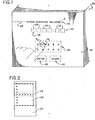
- FIG. 1 illustrates diagrammatically a touch-sensitive overlay in accordance with the present invention, designated generally as 20, associated with a CRT display identified as 22.
- the display 22 is a cathode ray tube (CRT) display for a host computer system (not shown), such as a home computer programmed to provide the user with a number of general purpose routines--in this illustration, one for balancing a bank account.
- CTR cathode ray tube
- touch-sensitive overlays are used in a much broader range of applications, including some very sophisticated utilities. Nonetheless, the basic principles of the overlay of the present invention are equally applicable regardless of that consideration, as will be appreciated as this description ensues.
- the CRT display 22 provides a visual display of luminous characters as a raster 24 scans across and thence sequentially down the display screen.
- a raster 24 scans across and thence sequentially down the display screen.
- about 200 display lines are provided downwardly across the face of the screen, with about three such raster lines being illuminated at any given time, due to and depending upon the persistence of the phosphor comprising the screen itself.
- the raster 24 is generally capable of developing a luminous character anywhere within the confines of the screen of CRT display 22 and, accordingly, character information latently may occupy any of a plurality of the character locations defined by the scanning raster.
- a field 26 is defined as being eight dot locations in width and 14 scan lines in height with a reduced character field 28 being limited within the broader confines of field 26 as an area having a width of seven dots and a height of nine scan lines; these individual character locations being considered in somewhat greater detail below.
- the host system has presented through the CRT display 22 an instructional step "ENTER BEGINNING BALANCE" within a field identified as 30.
- a field 32 comprised of latent character locations 34 within which will be entered the required balance information.
- a cursor 36 appears beneath that character location 34 within which a selected digit is to appear, the digit "1" having been entered by the user in the first location. That information is entered within the field 32 by the user touching the corresponding digit location within a field 38, as shown in phantom where the user's finger is applied to the digit "1".
- the cursor 36 will index to the next character location 34 and the appropriate digit entered therein in the same manner, by touching the proper location within the field 38.
- the user may touch a field 40 bearing the legend "ENTER” in order to transfer the balance information to the host system.
- the display may then present an instructional step for the user to load withdrawals from the account in order to continue with the routine.
- an area 42 bearing the legend "CLEAR” is provided to reset the field 32 in order to enter correct information.
- the user interacts with the host system simply by observing a display on the CRT 22 and touching the overlay 20 in the manner directed by the system, greatly simplifying interaction and broadening the population of potential system users.
- FIG. 3 is a sectional view showing the touch-sensitive overlay 20 in cooperative, optically proximate engagement with the CRT display 22.
- the overlay 20 is comprised of a photoreactive transducer designated generally as 44 which serves to convert luminous character information within the position-multiplexed array of-characters appearing on the CRT 22 into a measurable photoelectric response.
- a wide range of photoreactive transducers may be employed for this purpose provided the same are characterized as having at least one photoelectric parameter which varies as a function of incident light from the display 22.
- the transducer 44 responds to the presence of incident light from luminous characters on the display 22 as represented generally at positions 46, 48, and 50.
- the photoelectric response may equally well be correlated to the absence of luminous information at a given location as detected by a change in a steady state conditon existing therein.
- the photoreactive transducer 44 is comprised of a mask of an open photovoltaic cell 52 shown here to be a continuous mask of a photovoltaic semiconductor having a first compositional layer 54 separated from a second compositional layer 56 by a junction 58.
- the junction 58 in this embodiment is a light-responsive p-n (or n-p) semiconductor junction.
- the incident light from the locations 46, 48 and 50 striking the junction 58 will cause the creation of electron/hole pairs as is conventional in semiconductor devices of this sort resulting, in turn, in the development of a localized potential across the cell 52.
- the photovoltaic cell 52 is borne upon a thin-film 60 of an optically transparent, electrically conductive material.
- the film 60 is supported upon a-substrate 62, in this case -the standard .implosion plate -conventionally associated with a CRT tube.
- the implosion plate 62 is bonded to the face of the CRT 22 by a polymeric medium 64 as is also conventional.
- the cell 52 is an open photovoltaic cell as shown in the embodiment of Figure 3. Accordingly, the development of the localized potentials at the regions of the junction 58 in response to the incident light will remain static.
- An outer cell electrode designated generally as 66 is included in this embodiment for the purpose of completing the cell in order to generate a usable voltage pulse indicative of a position touched by the operator.
- the outer cell electrode shown in Figure 3 is comprised of a thin film 68 of an optically transparent, electrically conductive material supported upon a flexibly resilient substrate 70 which also possesses optical transparency.
- the cell electrode 66 is disposed in spaced relationship from the cell 52 by peripheral spacer means 72 in order to yield a gap or void area 74 between these components.
- a plurality of non-conductive spacers 76 are screened or otherwise deposited upon the inner surface of the film 68 in an array about its interior dimensions to guard against an inadvertent contact and thereby insure that only the positive touch by the operator, as shown in phantom lines, results in contact between the outer cell electrode 66 and the open cell 52.
- the raster scan is very fast, sweeping the entire display usually at 50 or 60 complete scans per second where each scan is comprised of, e.g., 224 individual scan lines.
- each scan is comprised of, e.g., 224 individual scan lines.
- the presence of a luminous character at point 48 will allow that voltage i developed in the photocell 52 to appear across-zthe load resistor 78; the configuration of the pulse being a function of, inter alia, the speed and persistence of the phosphor employed and the relative size of the load resistance 78 vis-a-vis the surface resistivity of the components constituting the transducer 44.
- the voltage pulse developed across resistor 78 is then utilized to interrogate the CRT controller as described more fully below in order to identify the precise location of the raster scan at the time the pulse occurs. This yields the ability to discriminate spatially the location corresponding to the point 48 from, e.g., those points identified 46 and 50 simply by touching that point..
- the ability to achieve spatial discrimination in the context of the embodiment of Figure 3 can be made within very exacting dimensional limits.
- the raster scan maintains approximately three luminous scan lines at any point in time, progressing downwardly for each complete scan of the face of the CRT 22.
- the speed of scanning in combination with the persistence of the phosphor gives the appearance of a relatively continuous presentation of luminous character information on the screen.
- each character location has a height,greater than the three scan line illumination normally provided; leading to excellent vertical discrimination of one character location from another.
- Horizontal discrimination i.e., along the same scan line
- That threshold is achieved, in part, by selecting the value of the load resistance 78 in light of the lineal resistivity of the transducer 44, and principally the layer 56, with due consideration for the speed of both the rise and decay of the phosphor employed on the CRT screen. More specifically, and with reference to Figure 1, the physical location between the digits "1" and “2" may be represented by an equivalent resistor R S which will vary both with respect to the composition of the cell 52 and the dimensional separation of the two locations. A similar condition obtains in respect of the difference in position between the digit "O" and the selected digit "1" for this example. As the raster scans across a line through the first row of digits in field 38, a localized potential will be developed at each illuminated location.
- Figure 4 illustrates schematically the equivalent circuit for the overlay 20 and the interfacing electronics between it and the CRT controller for the display 22; pointing up the elegant simplicity of the system.
- the overlay 20 is shown within a dashed outline to be comprised of an equivalent photodiode 52 and a switch contact representing the outer cell electrode 66.
- the diode 52 Upon a manual touch of the outer cell electrode to complete the circuit and the coincident presence of the luminous character from point 48, the diode 52 will conduct and develop the voltage pulse across the load resistor 78, shown as R L in Figure 4.
- a filter shown in phantom and designated generally as 90 will be employed to reduce noise ⁇ appearing on the voltage pulse due, e.g., to horizontal retrace or simple common mode noise from other electrical apparatus in the vicinity of the device.
- the characteristic voltage pulse is applied as a first input to a comparator 92 while a reference voltage V REF developed across a reference resistor R R for establishing the desired threshold or enabling band width is applied as a second input to the comparator.
- a logic pulse output is achieved. That logic pulse is employed to interrogate the CRT controller, shown schematically in Figure 5.
- Figure 5 illustrates, and on a simplified basis, a conventional CRT controller and one which includes a light pen input noted in general above to be a rather standard feature in most commercial controller chips.
- the circuit includes a clock 94 which generates a train of pulses responsible for timing the scan of the raster.
- the clock output communicates with scan counters 96 for that purpose in order to control the position of the raster throughout and over its sweeps responsible for generating the display on the CRT 22.
- a first output from the counters 96 drives the raster while registers 98 receive location information monitoring the position of the raster over the course of time.
- a latch input 100 receives the logic pulse output of comparator 92 to interrogate the registers 98 for the purpose of reading the "instantaneous" location of the raster scan.
- FIG 6 illustrates an alternate but nonetheless highly preferred embodiment of a touch-sensitive overlay in accordance with the present invention, identified generally as 102.
- the overlay 102 is virtually the same as the overlay 20, save the deletion of the outer cell electrode 66 and the addition of a protective overcoating l04 directly upon the transducer cell 52.
- the construction of the overlay is the same and its functionality highly analogous to that described above with reference to Figure 3.
- the overcoat 104 in this embodiment is an optically transparent material and preferably one having dielectric characteristics. Its purpose is to protect the components of the photovoltaic cell 52 constituting the photoreactive transducer responsible for converting the light input from the display into a measurable electric quantity (in this case, an open cell electric potential).
- Elimination of the outer cell electrode carries with it the elimination of one of the lead lines, leaving but a single output 106 for communication with the interfacing circuitry.
- a manual touch by the operator completes the circuit, as shown in phantom where the operator's finger touches the overlay 104 outwardly proximate the illuminated location 48.
- the operator's body capacitance serves to develop the voltage pulse on output line 106 for creating a TTL- pulse used to interrogate the CRT controller previously described with reference to Figure 5.
- FIG. 7 shows schematically both the equivalent circuit for overlay 102 and the associated interface electronics--again evidencing the simplicity of the present invention in stark contrast to prior approaches to this end.
- the overlay 102 is shown within the phantom outline to be comprised of the photoresponsive cell 52 illuminated from point 48 on the CRT display.
- the capacitance of the display itself is represented by C in series with the capacitance of the operator's body identified as C o leading to ground.
- That pulse itself may then be applied to an AND gate 112 as a first input and to which is applied a blanking input allowing the gate to pass a pulse only during active trace time as opposed to retrace portions of the sweep.
- Another suggested approach is the inclusion of enable circuitry for the operational amplifier 108 allowing it to operate only during selected times. For example, due to the speed of raster scanning in a CRT, it is possible to dedicate one sweep to only the central portion of each character location such as that identified in phantom lines as 114 in Figure 2.
- the voltage pulse developed upon a manual touch of the overlay 102 is applied as shown in Figure 7 to the amplifier 108 but is capable of being processed to the TTL pulse only when that circuit is enabled by the presence of luminous information within the phantom zone 114 of the character location.
- the TTL pulse developed through the interface of Figure 7 is applied to the latch input 100 of the registers 98 in exactly the same manner as described above in order to identify the precise location touched by the operator for further processing by the host system.
- the embodiments of Figures 3 and 6 include a continuous mask of the photoreactive transducer extending entirely across the surface area of the visual display.
- a requirement of the photoreactive transducer is that it be optically transparent; that term connoting in this context transparency to a degree permitting visual perception of the display by the operator at a comfortable viewing level.
- a certain class of materials described more completely below in respect of fabrication of the instant overlay fulfills that requirement and also provides sufficient surface resistivity for the mask that horizontal discrimination of one character location from another may be achieved as noted hereinabove. Under certain circumstances, however, it may be found more advantageous or desirable to form the photoreactive transducer as a plurality of discrete cells disposed over the display in a cell array.
- the useful range of materials adaptable for the photoreactive transducer is considerably broadened by eliminating the constraint of optical transparency while nonetheless providing the desirable photoelectric response.
- forming the mask as a plurality of discrete cells isolated electrically one from another overcomes the need to be concerned with limitations on horizontal discrimination by effectively increasing the surface resistivity between cell locations to an, open circuit condition. Either or both of those functional requirements may be found by the skilled artisan to be of sufficient importance to warrant the fabrication of the overlay in the discrete cell form.
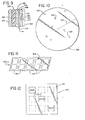
- Such a device is shown in Figures 8 and- 9.
- Figure 8 illustrates on an enlarged scale a portion of a touch-sensitive overlay designated generally as 120 comprised of a plurality of discrete photoreactive transducers 122 disposed in a spaced matrixed array, in this case an X-Y coordinate array.
- a spaced matrixed array in this case an X-Y coordinate array.
- the coordinate array for the presentation of data on the visual display to be, e.g., in a polar system, then it might be found desirable to conform the cell array to the same geometric bass.
- each of the cells 122 best viewed in Figure 9, functions in much the same manner as the continuous masks described above with reference to Figures 3 and 6.
- a display screen 124 presents an illuminated character or symbol at a point 126, the incident light beam traversing a bonding junction 128 between 'the display surface and a glass substrate 130 on which the cells 122 are formed.
- Each cell in this exemplary embodiment is again shown to be an open photovoltaic cell, comprised of a first layer 132 and a second layer 134 disposed across a light-responsive junction 136.
- Each cell 122 is preferably supported laterally within the cell array by an optically transparent film 138 which allows visual perception of the display 124 by the operator.
- the supporting layer 138 will be comprised of the precursor composition for each cell 122 which has been masked to prevent the formation of a photoreactive area outside the defined cell locations.
- the overlay 120- may include the same type of outer cell electrode as was associated with the embodiment of Figure 3 in order to provide a means for the operator to complete the open cell upon a manual touch. It is equally well envisioned that the overlay 120 will be completed by the deposition of an outer hard coat layer 140, as shown in phantom lines in Figure 9, to yield the same type of overlay described with reference to Figure 6, save the photoreactive transducer is now in the form of discrete cells vice the continuous cell described in respect thereof. Accordingly, a thin film 142 of an optically transparent, electrically conductive material will be provided intermediate the cells 122 and the supporting glass substrate 130 as will an associated single lead 144 to permit electrical communication between the cells 122 and the interface circuitry. In this instance, the same interface circuitry of Figure 7 may be employed to develop a TTL pulse for the purpose of interrogating the display controller in order to provide a means for identifying the position of the character location touched by the operator.
- each of the cells 122 may be optically transparent and, as the same are enveloped within an optically transparent layer 138, visual perception of the display information by the operator is readily accommodated.
- the components for or fabrication methodology of each cell 122 renders the same opaque or of such reduced optical transparency that visual perception is either unacceptably impeded or perhaps prevented altogher.
- cell size and spacing are important considerations in order to yield a useful display. It has been determined that a cell having a dimension on the order of about-0.005" will be found to provide a characteristic pulse recognizable by conventional circuit elements.
- the supporting material 138 possesses substantial electric resistance (approaching open circuit resistance) a fairly sharp voltage pulse may be developed as one cell enjoys electric isolation from adjacent cells when the most preferred sizing and spacing noted above are maintained.
- FIG 10 shows a conventional radar indicator designated generally as 150 having an overlay in accordance with the invention designated generally as 152.
- a raster 154 scans a circular path about the indicator 150 and provides illuminated target information as shown for example at point 156 and phantom points 158.
- the radar is one employed for controlling aircraft and the operator is in the process of routing an aircraft represented at point 156 to an airport location while maintaining appropriate awareness of aircraft identified in phantom at 158 as is expected within such an application.
- a host computer system is associated with the radar for the purpose of maintaining an accurate monitor on all aircraft within the zone surrounding the airport.
- the touch-sensitive overlay 152 allows the aircraft controller to apply a manual touch thereto at the indicated position of the aircraft at point 156 for the purpose of providing an input to the computer for identifying both the controller in communication with the aircraft and the precise aircraft being controlled. Such information may be utilized to whatever beneficial purpose might be desired by the system designer and warrants no further consideration herein. As respects the precise construction of the overlay 152, however, several points warrant specific mention.
- the same cooperative interrelationship between the indicator 150 and overlay 152 is established in the embodiment of Figure 10 as has been described hereinabove.
- the application of a manual touch to the desired character or symbol location (i.e., 156) and the coincident presence of luminous character information thereat as developed by the raster scan 154 will give rise to a recognizable signal useful for interrogating the raster scan circuitry and collateral identification of the precise point touched.
- the overlay 152 may be comprised of the same type of continuous cell as that of Figures 3 or 6, depending upon whether or not an outer cell electrode is included or omitted (respectively). Likewise, discrete cell locations may be established in the overlay 152 as shown in Figures 8 and 9.
- the geometry of the cell array conform to the same type of polar coordinate system as opposed to the X-Y matrix array shown in Figure 8.
- the individual cells in such a discrete cell array could be either optically transparent or opaque; in the latter case with due consideration for both sizing and spacing to insure adequate visual perception of the indicator by the operator.
- Figure 11 shows yet another alternate application for a touch-sensitive overlay in accordance with the present invention.
- the embodiments noted above employ a raster scan and associated scan control circuitry to provide a temporal base indicative of position-multiplexed character information on the visual display.
- Figure 11 represents a conventional "seven-segment" LED display employed in many applications to present alphanumeric information.
- the display of Figure 11, designated generally as 160 is shown to include five separate display locations each identified as 162.
- each character location contains the familiar seven-segment display of LED's as shown in phantom lines, which may be selectively illuminated to present a desired alphanumeric symbol; such as the numeral "7" shown in the last display position.
- a touch-sensitive overlay 164 in accordance with the present invention is disposed over and in optically proximate engagement with the LED display 160; the overlay 164 being shown in this exemplary embodiment to be a continuous mask of a photovoltaic cell such as the mask shown in Figures 3 or 6.
- a given one of the separate display locations may be identified, simply by the user's manual touch thereat and .the coincident presence of an illuminated alphanumeric character or other symbol.
- the time-multiplexing logic responsible for the illumination of the LED devices constituting that segment over the period of time when the touch is applied, will serve to identify the position touched by the operator.
- the overlay 164 is one including the outer cell electrode (as with the embodiment best viewed in Figure 3) a pair of contact points from the conductive films will communicate with the driving/control circuitry for the display; should the alternate embodiment omitting that electrode be selected, but a single contact -point - will - be required.
- discrete cells such as those described above with reference to Figures 8 and 9 may comprise the overlay 164; in which case it is most preferred to dispose at least one discrete cell optically proximate each of the elements in the seven-segment character location.
- a display panel identified generally as 170 is shown to contain a series of character locations identified as 172. In this example, nine such positions are shown, three of which bear the respective legends "RUN”, "STOP” and “TEST", while the balance of the nine positions remain in the event further options are required to be presented to the system operator.
- the display 170 is comprised of a back-lit panel where the level of illumination is sufficient to permit comfortable visual perception of the legends by the operator.
- a touch-sensitive overlay in accordance with the present invention, designated generally as 174, is disposed in cooperative, optically proximate engagement with the surface of the panel display 170 in order to permit operator interaction therewith.
- Each of the legends appearing in the array of panel 170 may simply be inscribed on the panel itself. In that case, the size of the panel will approximate that for a conventional single-function switch display; although the interface complexity is substantially reduced by supplanting a considerable portion of large wiring bundles or cables with but a single-.or double contact required by the instant overlay.
- legend locations 172 may be illuminated or, more preferably, simply the three corresponding to the choices presented.
- the most preferred method for the selective illumination of legend locations 172 is the selective sequencing of LED's associated with each position.
- a particular advantage of this approach is an entirely solid-state device of low power consumption, relying upon cycled LED's for illumination, LCD's for presentation, and the overlay of the present invention for interrogation.
- light wires communicating with an appropriate light source may be used for illumination and/or presentation of the legends or other character information.
- the operator may then make a suitable election among the choices presented which will be recognized upon a manual touch at the corresponding location. That touch and the coincident presence of back lighting will be recognized by the photoreactive transducer and, in turn, result in the generation of a characteristic logic pulse.
- the logic pulse communicates with the interfacing circuitry via either one or two contact points as may be required depending upon the embodiment selected for overlay 174.
- the overlay in accordance with the present invention is as easily fabricated as it is efficient in operation.
- the discussion which ensues exemplifies various suggested methods for producing the overlays disclosed herein.
- an overlay in accordance with the present invention is comprised of a photovoltaic cell (whether continuous or discrete) associated with a conventional CRT display
- fabrication is greatly facilitated.
- Most CRTs are provided with a glass implosion plate bonded or otherwise secured thereto to protect the face of the CRT and to protect those in its proximity in the event the same breaks (i.e., implodes).
- the first step is the deposition of a thin film of an optically transparent, electrically conductive material on the implosion plate.
- Various compositions meeting these functional requirements may be used, the preferred being tin oxide, indium-tin oxide and gold.
- Films as thin as about 2000-3000 Angstroms are now conventionally deposited and surface resistivity of less than 100 ohms per square achieved.
- the most preferred film is tin oxide deposited to yield surface resistivity on the order of about 30-50 ohms per square.
- the photovoltaic cell borne upon the, e.g., tin oxide film is most preferably fabricated in place. Where the continuous mask is selected, the cell must possess optical transmissibility at least to the extent allowing for visual perception of the underlying display by the operator.
- the most preferred cell is a cadmium sulfide/cuprous sulfide cell having a light-responsive p-n junction which will convert light information from the display to an electric potential.
- These types of cells are preferably fabricated by first depositing a layer of cadmium sulfide on the conductive substrate and then reacting same with cuprous chloride to convert the outer surface of the cadmium sulfide to cuprous sulfide and thereby yield the active junction. Other techniques are known in the art, and might be used to equal advantage.
- the same is comprised of an inner, thin film of an electrically conductive, optically transparent material deposited upon an optically transparent substrate.
- the conductive film may be, e.g., one of the same enumerated above--tin oxide, indium-tin oxide and gold, amongst others. It is preferably deposited upon a resilient polymeric substrate such as the material marketed under the trademark Mylar.
- the substrate polymer is preferably stretch-formed, in-order to provide it with the same radius of curvature as that of the CRT, prior to deposition of that conductive film.
- the outer cell electrode is bonded at the bezel along with the remaining components of the overlay with a peripheral spacer to maintain the needed separation between the electrode and cell. It may be found advantageous or otherwise desirable to include the plurality of non-conductive, intermediate spacers (76) about the inner surface of the cell electrode so that the same will not inadvertently be depressed against the cell and generate a spurious signal.
- a non-conductive material may be screened by conventional techniques onto the film after it has been deposited on the substrate in order to achieve that result.
- a hard coat of a dielectric material is applied over the top surface of the cell in order to protect the cell and also provide good response to the operator's touch for developing the characteristic logic pulse.
- a touch-sensitive overlay in accordance with the present invention where the photoreactive transducer is in the form of discrete cells is equally well a simple and straightforward task.
- Cell precursor material is first deposited upon the underlying film of, e.g., tin oxide and to that precursor is applied a photoresist leaving active areas where transducers are to be formed.
- the cells themselves do not provide such transmissibility the same will normally be sized on the order of about 0.005" in dimension (e.g., diameter) and spaced in the appropriate coordinate array (e.g., X-Y, polar).
- the precursor material in the non-active area may be stripped should the same lack suitable optical transmissibility or indeed may be retained if that is not the case.
- an outer cell electrode be elected for combination with the discrete cell transducer, it will be fabricated in the manner noted above; if that element is omitted, the same type of hard coating process noted above will then be employed.-Fabrication of overlays which employ other than a photovoltaic cell for the transducer follows conventional techniques in much the same way as noted above. For example, Schottky devices may be dd- posited in a desirable cell array to form a photoreactive mask following known techniques.
- Photo- resistive materials such as cadmium sulfide (which offers the added advantage of optical transparency) are of equal ease in terms of deposition to form the photoreactive member.
- transducer materials might be employed and, in some instances, departures from the exemplary techniques set forth above may be required. However, guided by the principles set forth herein, the skilled artisan will have no difficulty in designing and implementing a touch-sensitive overlay given the exigencies of the application at hand. * * * * * * * * * * * * * * * * * * * * * * * * * * * * * * * * * * * * * * * * * * * * * * * * * * * * * * * * * * * * * * * * * * * * * * * * * * * * * * * * * * * * * * * * * * * * * * * * * * * * * * * * * * * * * * * * * * * * * * * * * * * * * * * * * * * * * * * * * * * * * *
- the touch-sensitive overlays in accordance with one or more of the preferred embodiments set forth herein effectively overcome the drawbacks inhering in the conventional devices heretofore in use. Simplicity of fabrication and operation are hallmarks of the present design, as is a greatly reduced cost for implementation.
- the overlays of the present invention admit of a wide range of applications where character or symbol information is presented on a positioned-multiplexed basis in a manner whereby a photoreactive transducer will sense either the presence of luminous information or absence thereof in order to convert that condition into a measurable electric quantity which, in turn, serves to provide a characteristic logic pulse for determining that position.
Landscapes
- Engineering & Computer Science (AREA)
- General Engineering & Computer Science (AREA)
- Theoretical Computer Science (AREA)
- Human Computer Interaction (AREA)
- Physics & Mathematics (AREA)
- General Physics & Mathematics (AREA)
- Position Input By Displaying (AREA)
- Digital Computer Display Output (AREA)
Applications Claiming Priority (2)
| Application Number | Priority Date | Filing Date | Title |
|---|---|---|---|
| US06/448,947 US4567480A (en) | 1982-12-13 | 1982-12-13 | Touch-sensitive overlay |
| US448947 | 2006-06-07 |
Publications (2)
| Publication Number | Publication Date |
|---|---|
| EP0111879A2 true EP0111879A2 (fr) | 1984-06-27 |
| EP0111879A3 EP0111879A3 (fr) | 1986-12-30 |
Family
ID=23782272
Family Applications (1)
| Application Number | Title | Priority Date | Filing Date |
|---|---|---|---|
| EP83112539A Withdrawn EP0111879A3 (fr) | 1982-12-13 | 1983-12-13 | Couche à redéfinition de fonctions sensible au toucher |
Country Status (4)
| Country | Link |
|---|---|
| US (1) | US4567480A (fr) |
| EP (1) | EP0111879A3 (fr) |
| JP (1) | JPS59170932A (fr) |
| CA (1) | CA1244162A (fr) |
Cited By (3)
| Publication number | Priority date | Publication date | Assignee | Title |
|---|---|---|---|---|
| DE3628812A1 (de) * | 1985-09-26 | 1987-04-02 | Fluke Mfg Co John | Tastempfindliche kontakt-auflage |
| FR2593303A1 (fr) * | 1986-01-23 | 1987-07-24 | Dassault Electronique | Ecran tactile emulant un photostyle |
| EP0520655A3 (en) * | 1991-06-28 | 1993-11-18 | Ncr Int Inc | Item selection method and apparatus |
Families Citing this family (45)
| Publication number | Priority date | Publication date | Assignee | Title |
|---|---|---|---|---|
| JPS6066298A (ja) * | 1983-09-21 | 1985-04-16 | キヤノン株式会社 | 情報処理装置 |
| DE3565901D1 (en) * | 1984-04-04 | 1988-12-01 | Syrinx Innovations | Touch sensitive cathode ray tube |
| JPS613232A (ja) * | 1984-06-18 | 1986-01-09 | Casio Comput Co Ltd | 光学的入力装置 |
| US4758830A (en) * | 1984-10-25 | 1988-07-19 | Ti Corporate Services Limited | Switch/display units |
| US4814760A (en) * | 1984-12-28 | 1989-03-21 | Wang Laboratories, Inc. | Information display and entry device |
| US4740781A (en) * | 1985-02-08 | 1988-04-26 | Itt Gilfillan | Touch panel data entry device for thin film electroluminescent panels |
| US4716542A (en) * | 1985-09-26 | 1987-12-29 | Timberline Software Corporation | Method and apparatus for single source entry of analog and digital data into a computer |
| JPS63132323A (ja) * | 1986-08-27 | 1988-06-04 | テキサス インスツルメンツ インコ−ポレイテツド | データエントリー装置 |
| EP0272886A3 (fr) * | 1986-12-19 | 1990-12-19 | Pfu Limited | Système de traitement d'information d'image |
| US4734789A (en) * | 1987-02-02 | 1988-03-29 | Xerox Corporation | Editing copying machine |
| JPS63220334A (ja) * | 1987-03-10 | 1988-09-13 | Sharp Corp | デ−タ処理装置 |
| US4952932A (en) * | 1987-04-30 | 1990-08-28 | Canon Kabushiki Kaisha | Information input apparatus |
| US4786767A (en) * | 1987-06-01 | 1988-11-22 | Southwall Technologies Inc. | Transparent touch panel switch |
| US5053757A (en) * | 1987-06-04 | 1991-10-01 | Tektronix, Inc. | Touch panel with adaptive noise reduction |
| USD310663S (en) | 1987-09-29 | 1990-09-18 | Fedawa Wayne C | Computer aided design matrix menu for overlaying a digitizing tablet |
| USH716H (en) | 1987-11-16 | 1989-12-05 | Parallax induced pointing error avoidance method and means for systems using touch screen overlays | |
| JP2989607B2 (ja) * | 1988-03-30 | 1999-12-13 | キヤノン株式会社 | 情報入力装置 |
| US4931782A (en) * | 1988-06-24 | 1990-06-05 | E. I. Du Pont De Nemours And Company | Touch screen overlay with improved conductor durability |
| US4931019A (en) * | 1988-09-01 | 1990-06-05 | Pennwalt Corporation | Electrostatic image display apparatus |
| USD316708S (en) | 1989-03-10 | 1991-05-07 | Ncr Corporation | Activity display panel for a data processor or the like |
| US5093907A (en) * | 1989-09-25 | 1992-03-03 | Axa Corporation | Graphic file directory and spreadsheet |
| WO1991018383A1 (fr) * | 1990-05-23 | 1991-11-28 | Mann Brian M | Systeme de conception assistee par ordinateur utilisant une image de grande surface |
| US5149918A (en) * | 1990-10-29 | 1992-09-22 | International Business Machines Corporation | Touch sensitive overlay |
| DE4124541C2 (de) * | 1990-11-21 | 1993-10-14 | Yazaki Corp | Elektrischer Steckverbinder |
| WO1992013328A1 (fr) * | 1991-01-17 | 1992-08-06 | Rgb Dynamics | Ecran tactile capacitif |
| US5243332A (en) * | 1991-10-31 | 1993-09-07 | Massachusetts Institute Of Technology | Information entry and display |
| US5949348A (en) * | 1992-08-17 | 1999-09-07 | Ncr Corporation | Method and apparatus for variable keyboard display |
| US5378069A (en) * | 1992-08-24 | 1995-01-03 | Product Engineering & Mfg., Inc. | Environmentally safe touch typing keyboard |
| US5577848A (en) * | 1992-08-24 | 1996-11-26 | Bowen; James H. | Light controlled touch pad for cursor and selection control on a computer display |
| US5605406A (en) * | 1992-08-24 | 1997-02-25 | Bowen; James H. | Computer input devices with light activated switches and light emitter protection |
| US5936554A (en) * | 1996-08-01 | 1999-08-10 | Gateway 2000, Inc. | Computer input device with interactively illuminating keys |
| US6008784A (en) * | 1996-11-06 | 1999-12-28 | Acres Gaming Incorporated | Electronic display with curved face |
| US6512512B1 (en) * | 1999-07-31 | 2003-01-28 | Litton Systems, Inc. | Touch panel with improved optical performance |
| US6664744B2 (en) * | 2002-04-03 | 2003-12-16 | Mitsubishi Electric Research Laboratories, Inc. | Automatic backlight for handheld devices |
| US6871310B2 (en) * | 2002-06-03 | 2005-03-22 | Fujitsu Limited | Binary time-frame expansion of sequential systems |
| JP2004014383A (ja) * | 2002-06-10 | 2004-01-15 | Smk Corp | 接触式入力装置 |
| US7352355B2 (en) * | 2002-10-28 | 2008-04-01 | Delphi Technologies, Inc. | Transparent overlay input device |
| DE10352714A1 (de) * | 2003-11-05 | 2005-07-07 | E.G.O. Elektro-Gerätebau GmbH | Bedieneinrichtung |
| TWM352088U (en) * | 2008-08-12 | 2009-03-01 | Cando Corp | Sensory structure of capacitive touch panel with predetermined sensing areas |
| TWI486834B (zh) * | 2012-11-07 | 2015-06-01 | Chih Chung Lin | 具光電轉換之觸控裝置 |
| TWI484390B (zh) * | 2012-11-07 | 2015-05-11 | Chih Chung Lin | 具光電轉換之觸控模組 |
| TWI461896B (zh) * | 2012-11-07 | 2014-11-21 | Chih Chung Lin | 具光電轉換之觸控面板 |
| CN103809789A (zh) * | 2012-11-07 | 2014-05-21 | 林志忠 | 具光电转换的触控面板 |
| CN103729096A (zh) * | 2013-12-25 | 2014-04-16 | 京东方科技集团股份有限公司 | 交互识别系统以及显示装置 |
| US9787934B2 (en) * | 2014-01-15 | 2017-10-10 | Apple Inc. | Wireless devices with touch sensors and solar cells |
Family Cites Families (8)
| Publication number | Priority date | Publication date | Assignee | Title |
|---|---|---|---|---|
| US3737668A (en) * | 1970-07-30 | 1973-06-05 | Marconi Co Ltd | Keyboard |
| NL7409823A (nl) * | 1973-07-31 | 1975-02-04 | Fujitsu Ltd | Uitvoerinrichting voor informatie omtrent cooerdinatenposities. |
| US4177354A (en) * | 1978-04-17 | 1979-12-04 | Bell Telephone Laboratories, Incorporated | Graphic communications apparatus |
| US4319331A (en) * | 1980-01-28 | 1982-03-09 | Nestor Associates | Curve follower |
| SE441870B (sv) * | 1980-04-16 | 1985-11-11 | Western Electric Co | Beroringskenslig anordning for anvendning tillsammans med en signalkella |
| US4484179A (en) * | 1980-04-16 | 1984-11-20 | At&T Bell Laboratories | Touch position sensitive surface |
| US4305071A (en) * | 1980-04-16 | 1981-12-08 | Bell Telephone Laboratories, Incorporated | Touch sensitive screen signal detection arrangement |
| US4396977A (en) * | 1980-06-16 | 1983-08-02 | Forney Engineering Company | Industrial process control system |
-
1982
- 1982-12-13 US US06/448,947 patent/US4567480A/en not_active Expired - Lifetime
-
1983
- 1983-12-13 JP JP58234929A patent/JPS59170932A/ja active Pending
- 1983-12-13 EP EP83112539A patent/EP0111879A3/fr not_active Withdrawn
- 1983-12-13 CA CA000443166A patent/CA1244162A/fr not_active Expired
Cited By (3)
| Publication number | Priority date | Publication date | Assignee | Title |
|---|---|---|---|---|
| DE3628812A1 (de) * | 1985-09-26 | 1987-04-02 | Fluke Mfg Co John | Tastempfindliche kontakt-auflage |
| FR2593303A1 (fr) * | 1986-01-23 | 1987-07-24 | Dassault Electronique | Ecran tactile emulant un photostyle |
| EP0520655A3 (en) * | 1991-06-28 | 1993-11-18 | Ncr Int Inc | Item selection method and apparatus |
Also Published As
| Publication number | Publication date |
|---|---|
| JPS59170932A (ja) | 1984-09-27 |
| EP0111879A3 (fr) | 1986-12-30 |
| CA1244162A (fr) | 1988-11-01 |
| US4567480A (en) | 1986-01-28 |
Similar Documents
| Publication | Publication Date | Title |
|---|---|---|
| US4567480A (en) | Touch-sensitive overlay | |
| KR100942293B1 (ko) | 광을 이용한 터치 센싱 방법 및 그에 따른 터치패널 장치와시스템 | |
| US4310839A (en) | Interactive display system with touch data entry | |
| US4484179A (en) | Touch position sensitive surface | |
| US7952564B2 (en) | Multiple-touch sensor | |
| US4954823A (en) | Touch keyboard systems | |
| EP0165548B1 (fr) | Petit appareil électronique comportant un système d'entrée optique | |
| KR100325381B1 (ko) | 지문입력기를 이용한 터치패드 구현방법 및지문입력기능을 하는 터치패드 장치 | |
| US5319386A (en) | Ideographic character selection method and apparatus | |
| US8665223B2 (en) | Display device and method providing display contact information based on an amount of received light | |
| US5736976A (en) | Computer data entry apparatus with hand motion sensing and monitoring | |
| US8373679B2 (en) | Infrared touchscreen electronics | |
| US20030006972A1 (en) | Touch panel with improved optical performance | |
| EP0802500A2 (fr) | Capteur tactile sans coussin | |
| US20100214135A1 (en) | Dynamic rear-projected user interface | |
| US20100097323A1 (en) | Hydrogel-based tactile-feedback touch screen | |
| US20040189612A1 (en) | Touch sensor using light control | |
| JPH01136227A (ja) | タツチ・パネル | |
| Pfauth et al. | Person-computer interface using touch screen devices | |
| CN109508119A (zh) | 悬浮触控显示装置及悬浮触控方法 | |
| JPH11119898A (ja) | タッチパネル | |
| JPH1091348A (ja) | 座標入力装置および液晶表示装置 | |
| KR840002277B1 (ko) | 접촉 위치 감지 장치 | |
| JP2000132317A (ja) | エリアセンサ及びエリアセンサを用いた入力装置 | |
| JP2876825B2 (ja) | 光タブレット |
Legal Events
| Date | Code | Title | Description |
|---|---|---|---|
| PUAI | Public reference made under article 153(3) epc to a published international application that has entered the european phase |
Free format text: ORIGINAL CODE: 0009012 |
|
| AK | Designated contracting states |
Designated state(s): DE FR GB IT NL SE |
|
| PUAL | Search report despatched |
Free format text: ORIGINAL CODE: 0009013 |
|
| AK | Designated contracting states |
Kind code of ref document: A3 Designated state(s): DE FR GB IT NL SE |
|
| STAA | Information on the status of an ep patent application or granted ep patent |
Free format text: STATUS: THE APPLICATION IS DEEMED TO BE WITHDRAWN |
|
| 18D | Application deemed to be withdrawn |
Effective date: 19870101 |
|
| RIN1 | Information on inventor provided before grant (corrected) |
Inventor name: BLANCHARD, RANDALL DEAN |