EP0112062A2 - Halbleiterspeicher - Google Patents
Halbleiterspeicher Download PDFInfo
- Publication number
- EP0112062A2 EP0112062A2 EP83307052A EP83307052A EP0112062A2 EP 0112062 A2 EP0112062 A2 EP 0112062A2 EP 83307052 A EP83307052 A EP 83307052A EP 83307052 A EP83307052 A EP 83307052A EP 0112062 A2 EP0112062 A2 EP 0112062A2
- Authority
- EP
- European Patent Office
- Prior art keywords
- memory
- decoder
- sets
- cells
- decoders
- Prior art date
- Legal status (The legal status is an assumption and is not a legal conclusion. Google has not performed a legal analysis and makes no representation as to the accuracy of the status listed.)
- Withdrawn
Links
- 230000015654 memory Effects 0.000 title claims abstract description 52
- 239000004065 semiconductor Substances 0.000 title description 3
- 230000003068 static effect Effects 0.000 claims abstract description 7
- 238000003491 array Methods 0.000 claims description 13
- 230000005669 field effect Effects 0.000 claims description 5
- 238000000034 method Methods 0.000 claims description 2
- 239000000872 buffer Substances 0.000 description 3
- 230000000694 effects Effects 0.000 description 3
- 230000000295 complement effect Effects 0.000 description 1
- 238000010276 construction Methods 0.000 description 1
- 230000006735 deficit Effects 0.000 description 1
- 238000010586 diagram Methods 0.000 description 1
- 238000007599 discharging Methods 0.000 description 1
Images


Classifications
-
- G—PHYSICS
- G11—INFORMATION STORAGE
- G11C—STATIC STORES
- G11C11/00—Digital stores characterised by the use of particular electric or magnetic storage elements; Storage elements therefor
- G11C11/21—Digital stores characterised by the use of particular electric or magnetic storage elements; Storage elements therefor using electric elements
- G11C11/34—Digital stores characterised by the use of particular electric or magnetic storage elements; Storage elements therefor using electric elements using semiconductor devices
- G11C11/40—Digital stores characterised by the use of particular electric or magnetic storage elements; Storage elements therefor using electric elements using semiconductor devices using transistors
- G11C11/41—Digital stores characterised by the use of particular electric or magnetic storage elements; Storage elements therefor using electric elements using semiconductor devices using transistors forming static cells with positive feedback, i.e. cells not needing refreshing or charge regeneration, e.g. bistable multivibrator or Schmitt trigger
- G11C11/413—Auxiliary circuits, e.g. for addressing, decoding, driving, writing, sensing, timing or power reduction
- G11C11/417—Auxiliary circuits, e.g. for addressing, decoding, driving, writing, sensing, timing or power reduction for memory cells of the field-effect type
- G11C11/418—Address circuits
-
- G—PHYSICS
- G11—INFORMATION STORAGE
- G11C—STATIC STORES
- G11C8/00—Arrangements for selecting an address in a digital store
- G11C8/10—Decoders
Definitions
- This invention relates to semiconductor memories and in particular to static random access memories.
- Semiconductor memories e.g. of the NMOS static random access types store data in the form of binary digits in arrays of memory cell. Retrieval of this data is effected via decoder circuits which access a particular cell or cells to be read. It will be apparent that, to prevent data corruption, the decoder output signals corresponding to the cells to be accessed must not introduce overlapping of adjacent signals or there will be a risk of data corruption caused by accessing two cells at once.
- the memory cells are arranged in a two-dimensional array of m rows and n columns. This array may be physically divided into 2 or more sub-arrays for layout or operating reasons.
- a cell is accessed by means of X-decoders and Y-decoders which connect the cell to the input/output circuitry. Thus there are m X-decoders and n Y-decoders.
- a static random access memory including sets of memory cells, characterised in that said memory cells are divided logically into two or more sets, that row-decoder sets are provided one for each memory cell set whereby the cells of that set can be accessed, and that means are provided whereby, when a memory cell is accessed, power is supplied only to that one of the decoder sets corresponding to the accessed cell.
- the memory cells are laid out in two similar arrays, but in some applications a larger number of subdivisions may be employed.
- the memory is fabricated by a high speed high density n-channel HMOS process.
- the decoder circuit includes a plurality of field effect transistors, one for each address input and each coupled between the circuit ground and a decoding node.
- Voltage clamp means limits the voltage of the decoding node to a value significantly less than the circuit supply voltage.
- the memory which comprises a static random access memory, includes two similar arrays of memory cells 11 having a columnar array of X -decoders 12 disposed therebetween. Two similar sets of Y-decoders 13 are disposed at the one end of the cell arrays 11. An individual memory cell lla is accessed by providing the decoders 12 and 13 with the corresponding X and Y address via X-address and Y-address buffers 14 and 15 respectively. Note that Fig. 1 shows the physical rather than the electrical layout of the memory.
- the memory is a 16K word by one bit memory with the memory cells physically arranged in two 128 by 64 arrays.
- each array (11) has 128 X -decoders in the X-decoder array (12) and 64 Y-decoders in each of the Y-decoder arrays (13).
- This physical arrangement is the result of layout considerations. Electrically the array is not split in the Y direction.
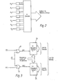
- Figs. 2 and 3 illustrate the operation of the X -decoder circuits.
- an X-address in the form of a seven bit binary code is fed to the X-address decoders which comprise two sets of 64 seven input NOR gates, one set being used for each memory array.-
- the address inputs are shown schematically as I o to I 6 in Fig. 2.
- Six of these inputs receive row address information, i.e. bits A to A 5 , whilst the seventh, e.g. I 6 , receives a decoder select bit A x . Since there are, in the present case, a total of 128, i.e.
- the X -decoders are logically divided into two sub-sets (23,24) using the X-address (Ax) as the controlling bit.
- Selection of one or other of the memory arrays is effected via a pair of two input NOR gates 31,32 ( F ig. 3).
- NOR gates 31,32 F ig. 3
- a x logic signal
- the other inputs of the NOR gates are coupled together and receive an enable signal CE, normally generated 'on chip', whereby power up and power down of the decoders is effected.
- the memory is held in a low power mode whilst the CE signal is high and reverts the normal operation when the CE signal is low.
- an X-decoder array can be activated only during the period when the CE signal is in its low state. Under such conditions a high A signal applied e.g. to the gate 31, and a corresponding low A x signal applied to the gate 32 causes generation of a low decoder disable signal DE2 at the output of gate 32 and a high decoder enable signal DE1 at the output of gate 31.
- DE1 and DE2 are used to power up X-decoder sub-sets 1 and 2 respectively. If a Decoder Enable signal is high then the corresponding X-decoder sub-set is powered up.
- DE If DE is low then the corresponding X-decoder sub-set reverts to a low power standby mode.
- CE if CE is high then both DE1 and DE2 are constrained to be low and the X-decoders are powered down with the rest of the memory. If CE is low then the rest of the memory is powered up for normal operation. Under such conditions, e.g. a high A x signal and a corresponding low Ax signal will result in the generation of a high DEI signal and a low DE2 signal.
- X-decoder sub-set 1 is powered up whilst sub-set 2 remains in low power standby. In this way only one of the decoder arrays corresponding to the required memory cell can be activated at any one time, and the decoder power requirements are thus effectively halved.
- the two arrays of X decoders are interleaved on the memory chip. This distributes the power dissipation and also minimises the effect of 'crosstalk' between adjacent decoders. It will of course be apparent to those skilled in the art that the physical division of the cells into two arrays does not correspond to their logical division into two or more sets of cells. It will also be clearly understood that although the arrangement is described with reference to the X-decoders where the greatest speed increase may be achieved it may also be applied to the Y-decoders.
- the decoder circuit includes a plurality of field effect transistors, T R1, TR2....TRN, one for each address input bit and each coupled between the circuit ground Vss and a decoding node DN.
- the arrangement is supplied via a current generator CG from a power supply Vcc, typically 5 volts:
- a voltage clamp VC may comprise one or more series connected field effect transistors, each with its gate connected to its drain.
- two transistors TR21, TR22 are used to provide a clamping level of e.g. 3 volts. Consequently both selection and particularly deselection of the decoder are faster as the decoding node has to be charged to and discharged from only 3 volts, i.e. a voltage significantly lower than the circuit supply voltage.
Landscapes
- Engineering & Computer Science (AREA)
- Microelectronics & Electronic Packaging (AREA)
- Computer Hardware Design (AREA)
- Static Random-Access Memory (AREA)
Applications Claiming Priority (4)
| Application Number | Priority Date | Filing Date | Title |
|---|---|---|---|
| GB08234844A GB2132843B (en) | 1982-12-07 | 1982-12-07 | Semiconductor memory |
| GB8234844 | 1982-12-07 | ||
| GB8236510 | 1982-12-22 | ||
| GB08236510A GB2133241B (en) | 1982-12-22 | 1982-12-22 | Memory decoder circuit |
Publications (2)
| Publication Number | Publication Date |
|---|---|
| EP0112062A2 true EP0112062A2 (de) | 1984-06-27 |
| EP0112062A3 EP0112062A3 (de) | 1986-10-08 |
Family
ID=26284617
Family Applications (1)
| Application Number | Title | Priority Date | Filing Date |
|---|---|---|---|
| EP83307052A Withdrawn EP0112062A3 (de) | 1982-12-07 | 1983-11-18 | Halbleiterspeicher |
Country Status (2)
| Country | Link |
|---|---|
| US (1) | US4616345A (de) |
| EP (1) | EP0112062A3 (de) |
Families Citing this family (2)
| Publication number | Priority date | Publication date | Assignee | Title |
|---|---|---|---|---|
| JP2511910B2 (ja) * | 1986-11-11 | 1996-07-03 | 三菱電機株式会社 | 半導体記憶装置 |
| EP0661814B1 (de) * | 1993-12-28 | 1999-03-31 | STMicroelectronics S.r.l. | Zähl-Ende Detektionsvorrichtung, insbesondere für nicht flüchtige Speicher |
Family Cites Families (8)
| Publication number | Priority date | Publication date | Assignee | Title |
|---|---|---|---|---|
| US3518449A (en) * | 1966-02-01 | 1970-06-30 | Texas Instruments Inc | Integrated logic network |
| DE2121865C3 (de) * | 1971-05-04 | 1983-12-22 | Ibm Deutschland Gmbh, 7000 Stuttgart | Speicher-Adressierschaltung |
| JPS522270A (en) * | 1975-06-24 | 1977-01-08 | Hitachi Ltd | Gate circuit |
| US4094012A (en) * | 1976-10-01 | 1978-06-06 | Intel Corporation | Electrically programmable MOS read-only memory with isolated decoders |
| US4096584A (en) * | 1977-01-31 | 1978-06-20 | Intel Corporation | Low power/high speed static ram |
| US4264828A (en) * | 1978-11-27 | 1981-04-28 | Intel Corporation | MOS Static decoding circuit |
| US4447895A (en) * | 1979-10-04 | 1984-05-08 | Tokyo Shibaura Denki Kabushiki Kaisha | Semiconductor memory device |
| JPS5857838B2 (ja) * | 1980-12-29 | 1983-12-22 | 富士通株式会社 | デコ−ド回路 |
-
1983
- 1983-11-18 EP EP83307052A patent/EP0112062A3/de not_active Withdrawn
- 1983-12-05 US US06/558,421 patent/US4616345A/en not_active Expired - Fee Related
Also Published As
| Publication number | Publication date |
|---|---|
| US4616345A (en) | 1986-10-07 |
| EP0112062A3 (de) | 1986-10-08 |
Similar Documents
| Publication | Publication Date | Title |
|---|---|---|
| JP3024687B2 (ja) | 半導体記憶装置 | |
| KR0140179B1 (ko) | 불휘발성 반도체 메모리 | |
| US5691945A (en) | Technique for reconfiguring a high density memory | |
| US6144582A (en) | Nonvolatile semiconductor memory device | |
| US4485460A (en) | ROM coupling reduction circuitry | |
| EP2132748B1 (de) | Decodierungssteuerung mit adressenübergangsdetektion in einer seitenlöschfunktion | |
| EP0142127A2 (de) | Redundante Schaltung für ein Halbleiterspeichergerät | |
| EP1070323B1 (de) | Seitenmoduslöschverfahren in flash-speichermatrize | |
| EP0622803B1 (de) | Adressenpuffer | |
| US4618784A (en) | High-performance, high-density CMOS decoder/driver circuit | |
| EP0249413B1 (de) | Halbleiterspeicheranordnung | |
| EP0327340B1 (de) | Dekodierschaltung | |
| US9275708B2 (en) | Row address decoding block for non-volatile memories and methods for decoding pre-decoded address information | |
| US6515911B2 (en) | Circuit structure for providing a hierarchical decoding in semiconductor memory devices | |
| US4818900A (en) | Predecode and multiplex in addressing electrically programmable memory | |
| US5719818A (en) | Row decoder having triple transistor word line drivers | |
| US5319595A (en) | Semiconductor memory device with split read data bus system | |
| US4723228A (en) | Memory decoding circuit | |
| KR910009408B1 (ko) | 반도체기억장치 | |
| US20040228188A1 (en) | Flash memory device with burst read mode of operation | |
| US4470133A (en) | Memory circuit having a decoder | |
| US4616345A (en) | Semiconductor memory | |
| EP0356983B1 (de) | Statische Speicheranordnung mit einer Signalgeneratorschaltung für sehr schnelle Vorladung | |
| EP0565024B1 (de) | Zeilendekodierer zum Antreiben einer Wortleitung in mehrernpunkten | |
| US5986946A (en) | Method and apparatus for reducing row shut-off time in an interleaved-row memory device |
Legal Events
| Date | Code | Title | Description |
|---|---|---|---|
| PUAI | Public reference made under article 153(3) epc to a published international application that has entered the european phase |
Free format text: ORIGINAL CODE: 0009012 |
|
| AK | Designated contracting states |
Designated state(s): DE FR IT NL |
|
| RAP1 | Party data changed (applicant data changed or rights of an application transferred) |
Owner name: STC PLC |
|
| PUAL | Search report despatched |
Free format text: ORIGINAL CODE: 0009013 |
|
| AK | Designated contracting states |
Kind code of ref document: A3 Designated state(s): DE FR IT NL |
|
| RAP1 | Party data changed (applicant data changed or rights of an application transferred) |
Owner name: STC PLC |
|
| STAA | Information on the status of an ep patent application or granted ep patent |
Free format text: STATUS: THE APPLICATION IS DEEMED TO BE WITHDRAWN |
|
| 18D | Application deemed to be withdrawn |
Effective date: 19870409 |
|
| RIN1 | Information on inventor provided before grant (corrected) |
Inventor name: MONK, TREVOR KENNETH |