EP0112111B1 - Solarzelle - Google Patents
Solarzelle Download PDFInfo
- Publication number
- EP0112111B1 EP0112111B1 EP83307383A EP83307383A EP0112111B1 EP 0112111 B1 EP0112111 B1 EP 0112111B1 EP 83307383 A EP83307383 A EP 83307383A EP 83307383 A EP83307383 A EP 83307383A EP 0112111 B1 EP0112111 B1 EP 0112111B1
- Authority
- EP
- European Patent Office
- Prior art keywords
- solar cell
- conductive layer
- transparent conductive
- amorphous silicon
- angstroms
- Prior art date
- Legal status (The legal status is an assumption and is not a legal conclusion. Google has not performed a legal analysis and makes no representation as to the accuracy of the status listed.)
- Expired - Lifetime
Links
- 239000002245 particle Substances 0.000 claims description 47
- 229910021417 amorphous silicon Inorganic materials 0.000 claims description 24
- AMGQUBHHOARCQH-UHFFFAOYSA-N indium;oxotin Chemical compound [In].[Sn]=O AMGQUBHHOARCQH-UHFFFAOYSA-N 0.000 claims description 12
- 239000000758 substrate Substances 0.000 claims description 11
- 230000002776 aggregation Effects 0.000 claims description 4
- 238000004220 aggregation Methods 0.000 claims description 4
- 239000012212 insulator Substances 0.000 claims description 2
- 238000006243 chemical reaction Methods 0.000 description 14
- 238000000151 deposition Methods 0.000 description 5
- 230000008021 deposition Effects 0.000 description 5
- 238000007738 vacuum evaporation Methods 0.000 description 5
- QVGXLLKOCUKJST-UHFFFAOYSA-N atomic oxygen Chemical compound [O] QVGXLLKOCUKJST-UHFFFAOYSA-N 0.000 description 4
- 229910052760 oxygen Inorganic materials 0.000 description 4
- 239000001301 oxygen Substances 0.000 description 4
- 239000000523 sample Substances 0.000 description 4
- XUIMIQQOPSSXEZ-UHFFFAOYSA-N Silicon Chemical compound [Si] XUIMIQQOPSSXEZ-UHFFFAOYSA-N 0.000 description 3
- 229910052782 aluminium Inorganic materials 0.000 description 3
- XAGFODPZIPBFFR-UHFFFAOYSA-N aluminium Chemical compound [Al] XAGFODPZIPBFFR-UHFFFAOYSA-N 0.000 description 3
- 239000004020 conductor Substances 0.000 description 3
- 229910052710 silicon Inorganic materials 0.000 description 3
- 239000010703 silicon Substances 0.000 description 3
- 239000013078 crystal Substances 0.000 description 2
- 238000007733 ion plating Methods 0.000 description 2
- 238000000034 method Methods 0.000 description 2
- 230000003287 optical effect Effects 0.000 description 2
- 238000000354 decomposition reaction Methods 0.000 description 1
- 230000001419 dependent effect Effects 0.000 description 1
- 238000001704 evaporation Methods 0.000 description 1
- 229910003437 indium oxide Inorganic materials 0.000 description 1
- PJXISJQVUVHSOJ-UHFFFAOYSA-N indium(iii) oxide Chemical compound [O-2].[O-2].[O-2].[In+3].[In+3] PJXISJQVUVHSOJ-UHFFFAOYSA-N 0.000 description 1
- 229910052751 metal Inorganic materials 0.000 description 1
- 239000002184 metal Substances 0.000 description 1
- 239000005361 soda-lime glass Substances 0.000 description 1
- 229910001220 stainless steel Inorganic materials 0.000 description 1
- 239000010935 stainless steel Substances 0.000 description 1
- XOLBLPGZBRYERU-UHFFFAOYSA-N tin dioxide Chemical compound O=[Sn]=O XOLBLPGZBRYERU-UHFFFAOYSA-N 0.000 description 1
- 229910001887 tin oxide Inorganic materials 0.000 description 1
Images
Classifications
-
- H—ELECTRICITY
- H10—SEMICONDUCTOR DEVICES; ELECTRIC SOLID-STATE DEVICES NOT OTHERWISE PROVIDED FOR
- H10F—INORGANIC SEMICONDUCTOR DEVICES SENSITIVE TO INFRARED RADIATION, LIGHT, ELECTROMAGNETIC RADIATION OF SHORTER WAVELENGTH OR CORPUSCULAR RADIATION
- H10F77/00—Constructional details of devices covered by this subclass
- H10F77/20—Electrodes
- H10F77/244—Electrodes made of transparent conductive layers, e.g. transparent conductive oxide [TCO] layers
-
- H—ELECTRICITY
- H10—SEMICONDUCTOR DEVICES; ELECTRIC SOLID-STATE DEVICES NOT OTHERWISE PROVIDED FOR
- H10F—INORGANIC SEMICONDUCTOR DEVICES SENSITIVE TO INFRARED RADIATION, LIGHT, ELECTROMAGNETIC RADIATION OF SHORTER WAVELENGTH OR CORPUSCULAR RADIATION
- H10F10/00—Individual photovoltaic cells, e.g. solar cells
- H10F10/10—Individual photovoltaic cells, e.g. solar cells having potential barriers
- H10F10/17—Photovoltaic cells having only PIN junction potential barriers
-
- H—ELECTRICITY
- H10—SEMICONDUCTOR DEVICES; ELECTRIC SOLID-STATE DEVICES NOT OTHERWISE PROVIDED FOR
- H10F—INORGANIC SEMICONDUCTOR DEVICES SENSITIVE TO INFRARED RADIATION, LIGHT, ELECTROMAGNETIC RADIATION OF SHORTER WAVELENGTH OR CORPUSCULAR RADIATION
- H10F71/00—Manufacture or treatment of devices covered by this subclass
- H10F71/138—Manufacture of transparent electrodes, e.g. transparent conductive oxides [TCO] or indium tin oxide [ITO] electrodes
-
- H—ELECTRICITY
- H10—SEMICONDUCTOR DEVICES; ELECTRIC SOLID-STATE DEVICES NOT OTHERWISE PROVIDED FOR
- H10F—INORGANIC SEMICONDUCTOR DEVICES SENSITIVE TO INFRARED RADIATION, LIGHT, ELECTROMAGNETIC RADIATION OF SHORTER WAVELENGTH OR CORPUSCULAR RADIATION
- H10F77/00—Constructional details of devices covered by this subclass
- H10F77/20—Electrodes
- H10F77/244—Electrodes made of transparent conductive layers, e.g. transparent conductive oxide [TCO] layers
- H10F77/247—Electrodes made of transparent conductive layers, e.g. transparent conductive oxide [TCO] layers comprising indium tin oxide [ITO]
-
- Y—GENERAL TAGGING OF NEW TECHNOLOGICAL DEVELOPMENTS; GENERAL TAGGING OF CROSS-SECTIONAL TECHNOLOGIES SPANNING OVER SEVERAL SECTIONS OF THE IPC; TECHNICAL SUBJECTS COVERED BY FORMER USPC CROSS-REFERENCE ART COLLECTIONS [XRACs] AND DIGESTS
- Y02—TECHNOLOGIES OR APPLICATIONS FOR MITIGATION OR ADAPTATION AGAINST CLIMATE CHANGE
- Y02E—REDUCTION OF GREENHOUSE GAS [GHG] EMISSIONS, RELATED TO ENERGY GENERATION, TRANSMISSION OR DISTRIBUTION
- Y02E10/00—Energy generation through renewable energy sources
- Y02E10/50—Photovoltaic [PV] energy
- Y02E10/548—Amorphous silicon PV cells
Definitions
- This invention relates to a solar cell for use in converting optical energy into electric energy.
- a conventional solar cell of the type described comprises first and second members opposite to each other and an amorphous silicon lamina between the first and the second members.
- the first and the second members serve as electrodes.
- a predetermined one of the first and second members should be transparent in order to expose the amorphous silicon lamina to light and to generate electromotive force across the first and second members.
- the solar cell has a high conversion efficiency of optical energy to electric energy.
- Most conventional attempts have been directed to improvement of characteristics of the amorphous silicon lamina so as to raise the conversion efficiency. In other words, the conventional attempts have left the first and the second members out of consideration.
- the conversion efficiency increases by improving characteristics of the amorphous silicon lamina to some extent. However, an increase of the conversion efficiency might reach a limit sooner or later in the above-mentioned manner.
- the conversion efficiency of each solar cell undesirably varies even when the amorphous silicon lamina is deposited on the same condition.
- FR-A-2514201 published 8 April 1983 mentions, in the part of the description concerning the prior art, a solar cell comprising a transparent electrode formed of particles whose average size is less than 50nm.
- a solar cell including a first member, a second member opposite said first member, and an amorphous silicon lamina connected between said first and said second members, a predetermined one of said first and said second members comprising a transparent conductive layer of indium tin oxide which comprises an aggregation of particles having an average particle size between 30 and 90 nm said particles being distributed in said transparent conductive layer with a particle density which is not smaller than ten per square micrometer
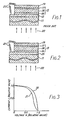
- Fig. 1 shows a sectional view of a conventional solar cell
- Fig. 2 diagrammatically shows a sectional view of a solar cell according to a first embodiment of this invention
- Fig. 3 shows voltage versus current characteristics of the conventional solar cell and the solar cell illustrated in Fig. 2;
- Fig. 4 shows a partial sectional view of the solar cell illustrated in Fig. 2;
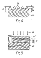
- Fig. 5 shows a sectional view of a solar cell according to a second embodiment of this invention.
- the illustrated solar cell has a transparent substrate 11 of an insulator having first and second principal surfaces directed upwards and downwards of this figure, respectively.
- the transparent substrate 11 may be of soda-lime glass.
- a transparent conductive layer 12 is coated on the first principal surface of the substrate 11 and serves as an electrode of the solar cell.
- a combination of the substrate 11 and the transparent conductive layer 12 may be called a first member.
- the transparent conductive layer 12 may selectively be removed to form a pattern, if necessary.
- An amorphous silicon lamina 13 is attached to the transparent conductive layer 12 and comprises a P-type amorphous silicon layer 16 brought into contact with the transparent conductive layer 12, an N-type amorphous silicon layer 17 opposite to the P-type silicon layer 16, and an intrinsic silicon layer 18 interposed between the amorphous silicon layers 16 and 17.
- An aluminum layer 19 is deposited on the N-type silicon layer 17 and may be called a second member serving as another electrode of the solar cell.
- a pair of conductors 21 are derived from the first and the second members to be connected to a load (not shown).
- the second principal surface of the substrate 11 is directed towards light indicated by arrows 22.
- the light 22 is incident onto the amorphous silicon lamina 13 through the transparent substrate 11 and the transparent conductive layer 12.
- the amorphous silicon lamina 13 is activated by the incidence of light to develop electromotive force across the transparent conductive layer 12 and the aluminum layer 19.
- the electromotive force is derived from the conductors 21 as electric power.
- a solar cell according to a first embodiment of this invention comprises similar parts designated by like reference numerals.
- the illustrated solar cell comprises a specific transparent conductive layer 25 which comprises tin-doped indium oxide, i.e. indium tin oxide.
- the illustrated indium tin oxide layer includes, by weight, 5% of tin oxide.
- the specific transparent conductive layer 25 is deposited to a thickness of 70nm (700 angstroms)by the use of vacuum evaporation and is formed by an aggregation of particles which have an average particle size not smaller than 30nm (300 angstroms).
- the vacuum evaporation is carried out with a pressure of oxygen and temperature of the substrate 11 kept at 10-4 Torr and 350°C, respectively.
- a deposition rate is about 0.15nm/s (1.5 angstroms/second).
- the particles are crystals of the indium tin oxide.
- the particles namely, the crystals are at first observed through a scanning electron microscope.
- the particle size of each particle is defined by a maximum dimension of each particle. For example, a diameter, a transverse axis, and a diagonal are defined as the particle sizes when the particles are circular, elliptical, and rectangular, respectively.
- a calculation is made of the total number and total size of all those particles whose particle size is not smaller than 20nm (200 angstroms). Thereafter, the total size is divided by the total number. In other words, such calculation takes no account of the other particles smaller than 20nm (200 anstroms).
- the illustrated conductive layer 25 has an average particle size of 30nm (300 angstroms).
- a sheet resistance of the specific transparent conductive layer 25 is about 30 ohms/ ⁇ .
- the specific transparent conductive layer 25 has an undulated or uneven surface, as diagrammatically illustrated in Fig. 2 to an exaggerated degree, and serves as the first member.
- an amorphous silicon lamina 13 is deposited on the specific transparent conductive layer 25 by the use of a glowdischarge decomposition method known in the art.
- An aluminum layer 19 which serves as the second member is formed on the amorphous silicon lamina 13 by vacuum evaporation.
- the conductors 21 are connected to the first and the second members, respectively.
- a curve 30 shows a voltage versus current characteristic of the solar cell illustrated in conjunction with Fig. 2.
- a curve 31 shows a similar characteristic of a reference solar cell as illustrated in Fig. 1.
- the reference solar cell comprises the indium tin oxide layer having the average particle size smaller than 20nm (200 angstroms).
- the indium tin oxide layer in the reference solar cell comprises particles most of which are smaller than 20nm (200 angstroms) and which never exceed 30nm (300 angstroms).
- Each characteristic is measured by exposing each of the solar cells to light of AM1 (Air Mass 1).
- the fill factor and the conversion efficiency of the solar cell according to this invention are improved by about 20% and 20% as compared with those of the conventional solar cell, respectively.
- the undulated conductive layer 25 serves to protect the light from being scattered from the amorphous silicon lamina 13. The light is therefore effectively utilized to excite the amorphous silicon lamina 13.
- an average particle size is adjustable by controlling the pressure of oxygen and the deposition rate with the substrate 11 kept at 350°C.
- an average particle size of 35nm (350 angstroms) can be obtained under a pressure of 266.10 - 4 Pa (2 x 10 - 4 Torr)and a deposition rate of 0.1nm/s of (1 angstrom/second) while an average particle size of 80nm of (800 angstroms) is attained under a pressure of 133.10 - 4Pa 10-4 Torr) and a disposition rate of 0.05nm/s of (0.5 angstrom/second).
- each particle is not smaller than 20nm (200 angstroms).
- a particular factor ⁇ has been introduced soas to determine an upper limit of the average particle size.
- the specific transparent conductive layer 25 undulates on a surface thereof and has therefore projections and notches on the surface. It is assumed that the thickness of the specific transparent conductive layer 25 is measured by the use of the usual thickness gauge of the probe type. In this event, the probe cannot be introduced into the notches and is in contact only with the projections because the probe is thicker than the width between the projections. As a result, the measured thickness specifies each height of the projections which is denoted by Ts.
- an average thickness Ta can be optically measured in a known manner.
- the above-mentioned particular factor ⁇ is defined by a difference between the thickness Ts of each projection and the average thickness Ta and may be called a difference factor.
- the difference factor has been between 10 and 65nm (100 and 650 angstroms), about 6% of the conversion efficiency has been accomplished and practically utilized as a solar cell.
- the difference factors ⁇ of 10 and 65nm (100 and 650 angstroms) correspond to the average particle sizes of about 30 and 90nm (300 and 900 angstroms), respectively.
- the average particle size is preferably not larger than 90nm (900 angstroms).
- a solar cell according to a second embodiment of this invention comprises, as the first electrode member, a conductive substrate 35 of a metal, such as stainless steel or the like.
- a specific transparent conductive layer 25' which is similar to that illustrated in conjunction with Fig. 2 is attached to the amorphous silicon lamina 13.
- the amorphous silicon lamina l3 is identical with that shown in Fig. 2.
- the specific transparent conductive layer 25' may be of indium tin oxide like in Fig. 2 and comprises an aggregation of particles which are not smaller in particle size than 30nm (300 angstroms).
- the transparent conductive layer 25' serves as the second member and is directed towards light 22, as shown in Fig. 5.
- a radio frequency (RF) reactive ion plating method may be carried out instead of the vacuum evaporation. In this event, it has been found out that the average particle size tends to increase with a reduction of RF power.
- the average particle sizes became substantially equal to 30, 50 and 80nm (300,500, and 800 angstroms) when the RF power was adjusted to 300, 200, and 100 watts, respectively, on condition that the substrate 11 or 35, the pressure of oxygen, and the deposition rate were kept at 300°C, 133.10 - 4Pa (1 x 10 - 4 Torr), and 0.3nm/s (3 angstroms/second), respectively.
Landscapes
- Photovoltaic Devices (AREA)
Claims (4)
- Solarzelle mit einem ersten Element, einem dem ersten Element gegenüberliegenden zweiten Element und einer zwischen dem ersten und dem zweiten Element liegenden Schicht aus amorphem Silizium, wobei ein vorgegebenes Element der beiden Elemente eine durchsichtige, leitende Schicht aus Indium-Zinn-Oxid aufweist, die eine Aggregation von Teilchen mit einer mittleren Teilchengröβe von 30 bis 90 nm aufweist und wobei die Teilchen in der durchsichtigen, leitenden Schicht mit einer Teilchendichte verteilt sind, die nicht kleiner ist als 10 µm-².
- Solarzelle nach Anspruch 1, wobei die Teilchendichte gröβer ist als 100 µm-².
- Solarzelle nach Anspruch 1 oder 2, wobei das erste Element das vorgegebene Element aus den beiden Elementen ist und ein durchsichtiges Isolatorsubstrat sowie die durchsichtige, leitende Schicht aufweist, die an der Schicht aus amorphem Silizium befestigt ist.
- Solarzelle nach Anspruch 1 oder 2, wobei das zweite Element das vorgegebene Element der beiden Elemente ist und durch die durchsichtige, leitende Schicht gebildet wird, die auf der Schicht aus amorphem Silizium liegt.
Applications Claiming Priority (2)
| Application Number | Priority Date | Filing Date | Title |
|---|---|---|---|
| JP213202/82 | 1982-12-04 | ||
| JP57213202A JPS59103384A (ja) | 1982-12-04 | 1982-12-04 | 太陽電池用透明導電膜 |
Publications (3)
| Publication Number | Publication Date |
|---|---|
| EP0112111A2 EP0112111A2 (de) | 1984-06-27 |
| EP0112111A3 EP0112111A3 (en) | 1985-04-10 |
| EP0112111B1 true EP0112111B1 (de) | 1991-03-06 |
Family
ID=16635221
Family Applications (1)
| Application Number | Title | Priority Date | Filing Date |
|---|---|---|---|
| EP83307383A Expired - Lifetime EP0112111B1 (de) | 1982-12-04 | 1983-12-05 | Solarzelle |
Country Status (5)
| Country | Link |
|---|---|
| US (1) | US4568791A (de) |
| EP (1) | EP0112111B1 (de) |
| JP (1) | JPS59103384A (de) |
| AU (1) | AU561774B2 (de) |
| DE (1) | DE3382192D1 (de) |
Families Citing this family (12)
| Publication number | Priority date | Publication date | Assignee | Title |
|---|---|---|---|---|
| US4689438A (en) * | 1984-10-17 | 1987-08-25 | Sanyo Electric Co., Ltd. | Photovoltaic device |
| US4798808A (en) * | 1986-03-11 | 1989-01-17 | Atlantic Richfield Company | Photoconductive device coontaining electroless metal deposited conductive layer |
| JP2706113B2 (ja) * | 1988-11-25 | 1998-01-28 | 工業技術院長 | 光電変換素子 |
| JP2740284B2 (ja) * | 1989-08-09 | 1998-04-15 | 三洋電機株式会社 | 光起電力素子 |
| FR2680279A1 (fr) * | 1991-08-09 | 1993-02-12 | Masse Georges | Dispositif thermo-electronique a hautes performances. |
| US5986206A (en) * | 1997-12-10 | 1999-11-16 | Nanogram Corporation | Solar cell |
| JP2001060702A (ja) * | 1999-06-18 | 2001-03-06 | Nippon Sheet Glass Co Ltd | 光電変換装置用基板およびこれを用いた光電変換装置 |
| IL153895A (en) * | 2003-01-12 | 2013-01-31 | Orion Solar Systems Ltd | Solar cell device |
| US8586861B2 (en) * | 2003-01-12 | 2013-11-19 | 3Gsolar Photovoltaics Ltd. | Solar cell device |
| US20060177567A1 (en) * | 2005-02-05 | 2006-08-10 | Winarski Tyson Y | Window that Generates Solar-powered Electricity via a Plurality of Noncontiguous Solar Cells |
| US9136404B2 (en) * | 2008-12-10 | 2015-09-15 | Iucf-Hyu (Industry-University Cooperation Foundation Hanyang University) | Solar cell capable of recycling a substrate and method for manufacturing the same |
| US20140150849A1 (en) * | 2012-11-30 | 2014-06-05 | Deutsche Cell Gmbh | Photovoltaic cell and method of production thereof |
Family Cites Families (4)
| Publication number | Priority date | Publication date | Assignee | Title |
|---|---|---|---|---|
| JPS5749278A (en) * | 1980-09-08 | 1982-03-23 | Mitsubishi Electric Corp | Amorphous silicone solar cell |
| CA1176740A (en) * | 1980-12-03 | 1984-10-23 | Yoshihisa Tawada | High-voltage photovoltaic cell having a hetero junction of amorphous semiconductor and amorphous silicon |
| JPS57126174A (en) * | 1981-01-27 | 1982-08-05 | Sumitomo Electric Ind Ltd | Thin film solar cell |
| JPS5857756A (ja) * | 1981-10-01 | 1983-04-06 | Agency Of Ind Science & Technol | 非晶質太陽電池 |
-
1982
- 1982-12-04 JP JP57213202A patent/JPS59103384A/ja active Pending
-
1983
- 1983-12-05 DE DE8383307383T patent/DE3382192D1/de not_active Expired - Fee Related
- 1983-12-05 US US06/558,111 patent/US4568791A/en not_active Expired - Lifetime
- 1983-12-05 AU AU21986/83A patent/AU561774B2/en not_active Ceased
- 1983-12-05 EP EP83307383A patent/EP0112111B1/de not_active Expired - Lifetime
Also Published As
| Publication number | Publication date |
|---|---|
| US4568791A (en) | 1986-02-04 |
| AU561774B2 (en) | 1987-05-14 |
| JPS59103384A (ja) | 1984-06-14 |
| EP0112111A2 (de) | 1984-06-27 |
| AU2198683A (en) | 1984-06-07 |
| DE3382192D1 (de) | 1991-04-11 |
| EP0112111A3 (en) | 1985-04-10 |
Similar Documents
| Publication | Publication Date | Title |
|---|---|---|
| EP1100130B1 (de) | Silizium dünnschicht photoelektrische vorrichtung | |
| EP0112111B1 (de) | Solarzelle | |
| AU694272B2 (en) | Photovoltaic element and method for producing the same | |
| EP0179556B1 (de) | Stromsammelstruktur für photovoltaische Elemente | |
| US5977476A (en) | High efficiency photovoltaic device | |
| EP1650812B1 (de) | Verfahren zur Herstellung einer Dünnschichtsiliziumsolarzelle | |
| US6008451A (en) | Photovoltaic device | |
| US5091764A (en) | Semiconductor device having a transparent electrode and amorphous semiconductor layers | |
| EP0684652B1 (de) | Photovoltaisches Bauelement, Elektrodenstruktur desselben und Herstellungsverfahren | |
| US5032884A (en) | Semiconductor pin device with interlayer or dopant gradient | |
| JP2783682B2 (ja) | 効率が改善されたタンデム形光起電力デバイスの製造方法および該方法により製造されたデバイス | |
| EP1189288B1 (de) | Photoelektrische umwandlungsanordnung | |
| CA1215456A (en) | Method for sputtering a pin amorphous silicon semi- conductor device having partially crystallized p and n-layers | |
| GB2044529A (en) | Amorphous silicon solar cells incorporating a thin insulating layer and a thin doped layer | |
| EP1119007A2 (de) | Leitfähige Paste und Solarzelle damit | |
| US4528418A (en) | Photoresponsive semiconductor device having a double layer anti-reflective coating | |
| EP0796498B1 (de) | Elektrochemische photovoltaische zelle | |
| US5064477A (en) | Radiant energy sensitive device and method | |
| JP3196155B2 (ja) | 光起電力装置 | |
| EP0321136B1 (de) | Sonnenzelle für niedrigen Lichtpegel | |
| JPH0566753B2 (de) | ||
| JP4562220B2 (ja) | 薄膜太陽電池 | |
| JP2001015780A (ja) | シリコン系薄膜光電変換装置用裏面電極、およびそれを備えたシリコン系薄膜光電変換装置 | |
| JP2975751B2 (ja) | 光起電力装置 | |
| JP3172368B2 (ja) | 光起電力装置 |
Legal Events
| Date | Code | Title | Description |
|---|---|---|---|
| PUAI | Public reference made under article 153(3) epc to a published international application that has entered the european phase |
Free format text: ORIGINAL CODE: 0009012 |
|
| AK | Designated contracting states |
Designated state(s): DE FR GB IT |
|
| PUAL | Search report despatched |
Free format text: ORIGINAL CODE: 0009013 |
|
| AK | Designated contracting states |
Designated state(s): DE FR GB IT |
|
| 17P | Request for examination filed |
Effective date: 19851007 |
|
| 17Q | First examination report despatched |
Effective date: 19870722 |
|
| GRAA | (expected) grant |
Free format text: ORIGINAL CODE: 0009210 |
|
| AK | Designated contracting states |
Kind code of ref document: B1 Designated state(s): DE FR GB IT |
|
| ITF | It: translation for a ep patent filed | ||
| ET | Fr: translation filed | ||
| REF | Corresponds to: |
Ref document number: 3382192 Country of ref document: DE Date of ref document: 19910411 |
|
| PLBE | No opposition filed within time limit |
Free format text: ORIGINAL CODE: 0009261 |
|
| STAA | Information on the status of an ep patent application or granted ep patent |
Free format text: STATUS: NO OPPOSITION FILED WITHIN TIME LIMIT |
|
| 26N | No opposition filed | ||
| PGFP | Annual fee paid to national office [announced via postgrant information from national office to epo] |
Ref country code: GB Payment date: 19961204 Year of fee payment: 14 |
|
| PGFP | Annual fee paid to national office [announced via postgrant information from national office to epo] |
Ref country code: FR Payment date: 19961230 Year of fee payment: 14 |
|
| PGFP | Annual fee paid to national office [announced via postgrant information from national office to epo] |
Ref country code: DE Payment date: 19970227 Year of fee payment: 14 |
|
| PG25 | Lapsed in a contracting state [announced via postgrant information from national office to epo] |
Ref country code: GB Free format text: LAPSE BECAUSE OF NON-PAYMENT OF DUE FEES Effective date: 19971205 |
|
| PG25 | Lapsed in a contracting state [announced via postgrant information from national office to epo] |
Ref country code: FR Free format text: THE PATENT HAS BEEN ANNULLED BY A DECISION OF A NATIONAL AUTHORITY Effective date: 19971231 |
|
| GBPC | Gb: european patent ceased through non-payment of renewal fee |
Effective date: 19971205 |
|
| PG25 | Lapsed in a contracting state [announced via postgrant information from national office to epo] |
Ref country code: DE Free format text: LAPSE BECAUSE OF NON-PAYMENT OF DUE FEES Effective date: 19980901 |
|
| REG | Reference to a national code |
Ref country code: FR Ref legal event code: ST |