EP0112662A1 - Gestapelte MOS-Bauelemente mit Verbindungen aus Polysilizium - Google Patents
Gestapelte MOS-Bauelemente mit Verbindungen aus Polysilizium Download PDFInfo
- Publication number
- EP0112662A1 EP0112662A1 EP83307265A EP83307265A EP0112662A1 EP 0112662 A1 EP0112662 A1 EP 0112662A1 EP 83307265 A EP83307265 A EP 83307265A EP 83307265 A EP83307265 A EP 83307265A EP 0112662 A1 EP0112662 A1 EP 0112662A1
- Authority
- EP
- European Patent Office
- Prior art keywords
- oxide
- metal
- semiconductor device
- further characterized
- drain
- Prior art date
- Legal status (The legal status is an assumption and is not a legal conclusion. Google has not performed a legal analysis and makes no representation as to the accuracy of the status listed.)
- Withdrawn
Links
Images

Classifications
-
- H—ELECTRICITY
- H10—SEMICONDUCTOR DEVICES; ELECTRIC SOLID-STATE DEVICES NOT OTHERWISE PROVIDED FOR
- H10P—GENERIC PROCESSES OR APPARATUS FOR THE MANUFACTURE OR TREATMENT OF DEVICES COVERED BY CLASS H10
- H10P14/00—Formation of materials, e.g. in the shape of layers or pillars
- H10P14/20—Formation of materials, e.g. in the shape of layers or pillars of semiconductor materials
- H10P14/24—Formation of materials, e.g. in the shape of layers or pillars of semiconductor materials using chemical vapour deposition [CVD]
-
- H—ELECTRICITY
- H10—SEMICONDUCTOR DEVICES; ELECTRIC SOLID-STATE DEVICES NOT OTHERWISE PROVIDED FOR
- H10P—GENERIC PROCESSES OR APPARATUS FOR THE MANUFACTURE OR TREATMENT OF DEVICES COVERED BY CLASS H10
- H10P14/00—Formation of materials, e.g. in the shape of layers or pillars
- H10P14/20—Formation of materials, e.g. in the shape of layers or pillars of semiconductor materials
- H10P14/38—Formation of materials, e.g. in the shape of layers or pillars of semiconductor materials characterised by treatments done after the formation of the materials
- H10P14/3802—Crystallisation or recrystallisation of non-monocrystalline semiconductor materials, e.g. regrowth
-
- H—ELECTRICITY
- H10—SEMICONDUCTOR DEVICES; ELECTRIC SOLID-STATE DEVICES NOT OTHERWISE PROVIDED FOR
- H10D—INORGANIC ELECTRIC SEMICONDUCTOR DEVICES
- H10D84/00—Integrated devices formed in or on semiconductor substrates that comprise only semiconducting layers, e.g. on Si wafers or on GaAs-on-Si wafers
- H10D84/01—Manufacture or treatment
- H10D84/02—Manufacture or treatment characterised by using material-based technologies
- H10D84/03—Manufacture or treatment characterised by using material-based technologies using Group IV technology, e.g. silicon technology or silicon-carbide [SiC] technology
- H10D84/038—Manufacture or treatment characterised by using material-based technologies using Group IV technology, e.g. silicon technology or silicon-carbide [SiC] technology using silicon technology, e.g. SiGe
-
- H—ELECTRICITY
- H10—SEMICONDUCTOR DEVICES; ELECTRIC SOLID-STATE DEVICES NOT OTHERWISE PROVIDED FOR
- H10D—INORGANIC ELECTRIC SEMICONDUCTOR DEVICES
- H10D88/00—Three-dimensional [3D] integrated devices
-
- H—ELECTRICITY
- H10—SEMICONDUCTOR DEVICES; ELECTRIC SOLID-STATE DEVICES NOT OTHERWISE PROVIDED FOR
- H10D—INORGANIC ELECTRIC SEMICONDUCTOR DEVICES
- H10D88/00—Three-dimensional [3D] integrated devices
- H10D88/01—Manufacture or treatment
-
- H—ELECTRICITY
- H10—SEMICONDUCTOR DEVICES; ELECTRIC SOLID-STATE DEVICES NOT OTHERWISE PROVIDED FOR
- H10P—GENERIC PROCESSES OR APPARATUS FOR THE MANUFACTURE OR TREATMENT OF DEVICES COVERED BY CLASS H10
- H10P14/00—Formation of materials, e.g. in the shape of layers or pillars
- H10P14/20—Formation of materials, e.g. in the shape of layers or pillars of semiconductor materials
- H10P14/29—Formation of materials, e.g. in the shape of layers or pillars of semiconductor materials characterised by the substrates
- H10P14/2901—Materials
- H10P14/2902—Materials being Group IVA materials
- H10P14/2905—Silicon, silicon germanium or germanium
-
- H—ELECTRICITY
- H10—SEMICONDUCTOR DEVICES; ELECTRIC SOLID-STATE DEVICES NOT OTHERWISE PROVIDED FOR
- H10P—GENERIC PROCESSES OR APPARATUS FOR THE MANUFACTURE OR TREATMENT OF DEVICES COVERED BY CLASS H10
- H10P14/00—Formation of materials, e.g. in the shape of layers or pillars
- H10P14/20—Formation of materials, e.g. in the shape of layers or pillars of semiconductor materials
- H10P14/34—Deposited materials, e.g. layers
- H10P14/3402—Deposited materials, e.g. layers characterised by the chemical composition
- H10P14/3404—Deposited materials, e.g. layers characterised by the chemical composition being Group IVA materials
- H10P14/3411—Silicon, silicon germanium or germanium
-
- H—ELECTRICITY
- H10—SEMICONDUCTOR DEVICES; ELECTRIC SOLID-STATE DEVICES NOT OTHERWISE PROVIDED FOR
- H10P—GENERIC PROCESSES OR APPARATUS FOR THE MANUFACTURE OR TREATMENT OF DEVICES COVERED BY CLASS H10
- H10P14/00—Formation of materials, e.g. in the shape of layers or pillars
- H10P14/20—Formation of materials, e.g. in the shape of layers or pillars of semiconductor materials
- H10P14/38—Formation of materials, e.g. in the shape of layers or pillars of semiconductor materials characterised by treatments done after the formation of the materials
- H10P14/3802—Crystallisation or recrystallisation of non-monocrystalline semiconductor materials, e.g. regrowth
- H10P14/3808—Crystallisation or recrystallisation of non-monocrystalline semiconductor materials, e.g. regrowth using laser beams
- H10P14/3814—Continuous wave laser beam
-
- H—ELECTRICITY
- H10—SEMICONDUCTOR DEVICES; ELECTRIC SOLID-STATE DEVICES NOT OTHERWISE PROVIDED FOR
- H10P—GENERIC PROCESSES OR APPARATUS FOR THE MANUFACTURE OR TREATMENT OF DEVICES COVERED BY CLASS H10
- H10P14/00—Formation of materials, e.g. in the shape of layers or pillars
- H10P14/20—Formation of materials, e.g. in the shape of layers or pillars of semiconductor materials
- H10P14/38—Formation of materials, e.g. in the shape of layers or pillars of semiconductor materials characterised by treatments done after the formation of the materials
- H10P14/3802—Crystallisation or recrystallisation of non-monocrystalline semiconductor materials, e.g. regrowth
- H10P14/382—Scanning of a beam
-
- H—ELECTRICITY
- H10—SEMICONDUCTOR DEVICES; ELECTRIC SOLID-STATE DEVICES NOT OTHERWISE PROVIDED FOR
- H10P—GENERIC PROCESSES OR APPARATUS FOR THE MANUFACTURE OR TREATMENT OF DEVICES COVERED BY CLASS H10
- H10P95/00—Generic processes or apparatus for manufacture or treatments not covered by the other groups of this subclass
-
- H—ELECTRICITY
- H10—SEMICONDUCTOR DEVICES; ELECTRIC SOLID-STATE DEVICES NOT OTHERWISE PROVIDED FOR
- H10W—GENERIC PACKAGES, INTERCONNECTIONS, CONNECTORS OR OTHER CONSTRUCTIONAL DETAILS OF DEVICES COVERED BY CLASS H10
- H10W20/00—Interconnections in chips, wafers or substrates
- H10W20/01—Manufacture or treatment
- H10W20/031—Manufacture or treatment of conductive parts of the interconnections
-
- H—ELECTRICITY
- H10—SEMICONDUCTOR DEVICES; ELECTRIC SOLID-STATE DEVICES NOT OTHERWISE PROVIDED FOR
- H10W—GENERIC PACKAGES, INTERCONNECTIONS, CONNECTORS OR OTHER CONSTRUCTIONAL DETAILS OF DEVICES COVERED BY CLASS H10
- H10W20/00—Interconnections in chips, wafers or substrates
- H10W20/40—Interconnections external to wafers or substrates, e.g. back-end-of-line [BEOL] metallisations or vias connecting to gate electrodes
- H10W20/41—Interconnections external to wafers or substrates, e.g. back-end-of-line [BEOL] metallisations or vias connecting to gate electrodes characterised by their conductive parts
- H10W20/44—Conductive materials thereof
- H10W20/4451—Semiconductor materials, e.g. polysilicon
Definitions
- This invention relates to stacked metal-oxide-semiconductor (MOS) devices and to a method for making them.
- VLSI very large scale integrated
- CMOS inverters having a common gate for both n- and p-channel transistors have been described by Gibbons et al, IEEE Electron Device Letters, EDL-1, page 11 et seq, and by Geoloe et al, IEDM, Washington, D.C. page 544 et seq, 1981.
- a stacked CMOS inverter more conducive to standard silicon integrated circuit fabrication techniques has been suggested by Colinge et al, IEEE Electron Device Letters, EDL-2, pages 250 et seq, 1981.
- n- and p-type transistors making up the inverter are stacked one on top of the other and have a common gate, a common drain and isolated sources.
- the top part of the common drain is laser annealed polysilicon which is essentially integral with a bottom part of the drain formed within the silicon substrate.
- an aluminum interconnect extends through a via within a SiO 2 coating overlying the common drain to connect the drain to a laterally offset bonding pad.
- One of the disadvantages of this structure is that during the contact sintering operation, or other higher temperature operations subsequent to metallization, spikes or spears of aluminum metal penetrate vertically or laterally into the silicon surrounding the contact windows. This can result in junction degradation or even shorting.
- a further disadvantage is that the drain region must be made somewhat larger than necessary for device operation simply to ensure that the interconnect via formed through the SiO 2 layer will lie over the drain.
- a stacked metal-oxide-semiconductor device is now proposed which eliminates the contact windows and aluminum interconnects.
- a stacked metal-oxide-semiconductor device having a first channel, source and drain within a silicon substrate, and a second channel, source and drain within a selectively recrystallized polysilicon layer formed above the substrate, said polysilicon layer having an additional recrystallized interconnect part extending from at least one of the upper source and drain to a laterally offset bonding pad.
- the stacked metal-oxide-semiconductor device can be a transistor in which the first and second sources are integral with one another, the first and second drains are integral with one another, and the channels are spaced from one another by a common gate formed within gate oxide.
- the MOS structure is a pair of transistors, for example, in a CMOS inverter arrangement, in which the first and second sources are integral with one another and the first and second drains are isolated from one another or a similar structure in which the drains are integral and the sources are isolated.
- a gate or gates controlling the channels also consist of recrystallized polysilicon.
- the recrystallized polysilicon in which the upper source, channel and drain are located functions as a second silicon substrate.
- appropriate oxide and polysilicon layers can be grown or deposited to form a transistor or transistors which have several possible channels or channel routes between them.
- the crystal orientation of the upper source, drain and channel is such as to form an essentially epitaxial continuation of the underlying source and drain within the substrate.
- the polysilicon in the upper source, drain and interconnect parts is rendered highly conductive by laser annealing and doping.
- a method of fabricating a stacked metal-oxide-semiconductor structure the steps of forming a first source region, a first drain region and a first channel region in a silicon substrate, forming a gate within an oxide layer overlying a first channel region extending between the source and drain regions, subsequently forming thereon a recrystallized polysilicon layer, and forming in the recrystallized polysilicon layer a second source region, a second drain region, a second channel region and an interconnect region extending away from at least one of said second source and drain regions to a bonding pad.
- Said at least one of the second source and drain regions can be made integral with an underlying corresponding one of the first source and drain regions.
- the method preferably includes the following additional steps.
- the second source and drain regions, a second channel region extending between the second source and drain regions and the or each interconnect region are formed by laser annealing and appropriately doping the polysilicon layer.
- the polysilicon is deposited by low pressure chemical vapour deposition over the complete wafer and then selectively etched following doping and laser annealing.
- the polysilicon layer is doped by ion implantation to provide an active top layer substrate and is recrystallized by laser annealing after deposition of an anti-reflective nitride coating on the polysilicon layer to cover the source, drain, top channel region and interconnects to the sites of bonding pads. Because that part of the polysilicon layer overlying the gate is thermally insulated from the substrate by gate oxide, then during laser annealing it is rendered hotter than the polysilicon overlying the substrate drain and source regions from which heat can more easily dissipate to the substrate. Thus on cooling, it solidifies later than the polysilicon around it and consequently seeded crystal conversion occurs first adjacent the substrate drain and source regions and later at the polysilicon over the gate.
- the substrate crystal orientation spreads throughout the recrystallized polysilicon within the top device active area.
- the nitride coating is removed and the second source and drain regions are formed for example by dopant pre-deposition and drive-in.
- Bonding pads are made by depositing a pyroglass layer over the wafer, opening windows through the pyroglass layer at appropriate sites, and depositing aluminum through the windows onto the distal ends of the interconnects and onto an extension of the common gate projecting out of the channel region.
- the aluminum deposits provide bonding pads for applying voltages to the device terminals.
- the gate which is prepared in an intermediate part of the process can also be prepared by laser annealing and doping a deposited polysilicon layer.
- the gate oxide is thermally grown in a two stage process, the first layer being grown on the substrate before deposition and formation of gate polysilicon and the second layer being grown on the gate following polysilicon deposition, doping, laser annealing and etching to define the gate.
- the gate is grown with a lateral projection extending out of the channel region to which a bonding pad can be electrically connected.
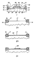
- an SMOS transistor 10 has a p-type silicon substrate 12.
- P +- type regions 14 underlie SiO 2 field oxide regions 16 which provide isolation from adjacent transistors (not shown).
- n -type source and drain regions 18 and 20 respectively.
- Extending between the source and drain regions and overlying the substrate is a first gate oxide layer 22.
- a recrystallized polysilicon gate 24 and a second gate oxide layer 26 Overlying the whole structure is a recrystallized polysilicon layer 28 which is doped to give source and drain regions 30 and 32 respectively contacting the source and drain regions 18 and 20 in the silicon substrate.
- p -type channel regions 34 and 36 Between the source and drain regions at respective levels are p -type channel regions 34 and 36.
- the recrystallized polysilicon layer 28 has interconnect regions 29 which connect the source and drain regions 30 and 32 to bonding pads 35.
- a central bonding pad is connected to a lateral extension of the gate 26.
- the Figure 1 device is a stacked n-channel enhancement mode transistor.
- a voltage applied to the common gate 26 induces an electric field within channel regions 34 and 36.
- the gate voltage is of proper polarity and magnitude a localized inversion layer is formed both above and below the gate to render the upper and lower channel regions conducting. Conduction takes place between sources and drains, the current depending on the gate voltage and the source to drain voltage. In effect the channel duty of the transistor is vertically shared between two channels.
- the Figure 1 transistor has two spaced channel regions 34 and 36 but there is no reason why, in principle, the transistors should not have more than two vertically spaced channels if further vertical integration is desired.
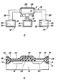
- a boron ion-implantation 14 is performed and field oxide 15 is grown using a known LOGOS technique and a first mask defining an area I ( Figure 3) to define a device well 17.
- a first gate oxide layer 22 is then thermally grown ( Figure 2b).
- a 7500A polysilicon layer is low pressure chemically vapour deposited at 625°C and then patterned to produce a common gate region 24 having a lateral projection 25.
- a phosphorus ion implantation technique is used to obtain n +- type doping in the regions 18 and 20.
- the polysilicon in the gate region is then recrystallized in a laser annealing step using an argon laser with a power output of about 6 watts, a beam diameter of 50 microns, and a scan rate of 50cm/second.
- the polysilicon structure is changed from small to large grains with a corresponding increase in conductivity.
- the laser annealing step is also used to drive the implanted phosphorus impurities into the gate, source and drain regions to render them highly conducting.
- a 1000A layer of top gate oxide is then thermally grown at 1050°C in dry oxygen and, using standard techniques, the gate oxide is selectively etched to expose the n -type source and drain regions 18 and 20 ( Figure 2f).
- a 7500A polysilicon layer 28 is low-pressure chemically vapour deposited at 625°C over the entire chip.
- the polysilicon is implanted with boron at a dosage of 5 x 10 11 /cm 2 at 60Kev to form an active p-type substrate for the upper channel 36 of ° the Figure 1 transistor.
- a 600A layer of-silicon nitride is then low-pressure chemically vapour deposited at 650°C and is defined using a third mask defining the area III ( Figure 3) so as to cover both the device well which extends between the isolating field oxide region 16, and interconnect regions 29 which extend from the source and drain to the sites 31.
- This layer functions as an anti-reflective coating during a subsequent selective laser annealing step using an argon laser with the previously cited operating conditions.
- the nitride layer ensures that the underlying polysilicon is melted during laser annealing.
- the polysilicon overlying the gate 24 since it is thermally insulated from the substrate by the gate oxide is hotter than that overlying the source and drain regions and consequently cools and crystallizes later.
- the substrate source and drain regions 18 and 20 therefore function to seed crystal conversion within the polysilicon layer 28, the crystal formation propagating away from the substrate source and drain regions into the channel region 36 overlying the gate 24.
- the anti-reflective coating is subsequently removed by etching using the third mask which defines area III ( Figure 3).
- a phosphorus ion implantation technique is then used to render n +- type the regions of the recrystallized polysilicon overlying the substrate source and drain ( Figure 2h).
- additional source and drain regions 30, 32 are formed in the polysilicon 28, these being integral with the source and drain regions 18 and 20 in the substrate.
- a fourth mask which defines the area IV is used to open contact windows 33 to the polysilicon at the outer bonding pad regions, and to the gate polysilicon at the projection 25.
- a fifth mask which defines an area V aluminum is chemically vapour deposited onto the outer ends of the polysilicon leads 29 to function as source and drain bonding pads. Simultaneously, aluminum is deposited to bridge the gate extension 25 and the site of a gate bonding pad.
- the invention has been described in terms of a stacked MOS device functioning as a single transistor, it will be appreciated that the invention can be used to advantage in alternative structures where a layer of polysilicon has been deposited and subsequently recrystallized in order to form an active substrate in which further MOS formations can be produced.
- the device has a common drain 20, 32 and isolated sources 18 and 30.
- Recrystallized polysilicon interconnects 29 are formed by appropriately doping and laser annealing regions of the polysilicon layer 28 so as to electrically connect the common drain and the top source to laterally offset bonding pads 35.
- Interconnects (not shown) to the lower source 18 and to the gate terminal 26 are conventionally made by aluminum evaporation through appropriately sited windows.
- the polysilicon interconnects 29 are relatively short.
- the sheet resistivity of polysilicon which is laser annealed and doped to a level of 10 21 carriers/cm 3 is 5 ⁇ / ⁇ which is sufficiently low for an interconnect material. Consequently although there is a small increase in terminal resistance, it is more than offset by lowering the risk of the substrate junctions being affected by aluminum penetration into the junctions and by the added degree of freedom afforded to the designer by not having to open windows to the source, drain or both.
Landscapes
- Metal-Oxide And Bipolar Metal-Oxide Semiconductor Integrated Circuits (AREA)
- Internal Circuitry In Semiconductor Integrated Circuit Devices (AREA)
Applications Claiming Priority (2)
| Application Number | Priority Date | Filing Date | Title |
|---|---|---|---|
| US45177182A | 1982-12-21 | 1982-12-21 | |
| US451771 | 1982-12-21 |
Publications (1)
| Publication Number | Publication Date |
|---|---|
| EP0112662A1 true EP0112662A1 (de) | 1984-07-04 |
Family
ID=23793620
Family Applications (1)
| Application Number | Title | Priority Date | Filing Date |
|---|---|---|---|
| EP83307265A Withdrawn EP0112662A1 (de) | 1982-12-21 | 1983-11-29 | Gestapelte MOS-Bauelemente mit Verbindungen aus Polysilizium |
Country Status (2)
| Country | Link |
|---|---|
| EP (1) | EP0112662A1 (de) |
| JP (1) | JPS59150479A (de) |
Cited By (1)
| Publication number | Priority date | Publication date | Assignee | Title |
|---|---|---|---|---|
| EP0331206A3 (de) * | 1988-03-04 | 1991-05-02 | Kabushiki Kaisha Toshiba | Integrierte Schaltungshalbleiteranordnung mit Mehrschicht-Verbindungsstruktur |
Families Citing this family (1)
| Publication number | Priority date | Publication date | Assignee | Title |
|---|---|---|---|---|
| JPS6484746A (en) * | 1987-09-28 | 1989-03-30 | Ricoh Kk | Semiconductor device |
Citations (1)
| Publication number | Priority date | Publication date | Assignee | Title |
|---|---|---|---|---|
| EP0021133A2 (de) * | 1979-06-06 | 1981-01-07 | Kabushiki Kaisha Toshiba | Halbleitervorrichtung mit einer Leiterbahnelektrode und Verfahren zu deren Herstellung |
-
1983
- 1983-11-29 EP EP83307265A patent/EP0112662A1/de not_active Withdrawn
- 1983-12-21 JP JP58239984A patent/JPS59150479A/ja active Pending
Patent Citations (1)
| Publication number | Priority date | Publication date | Assignee | Title |
|---|---|---|---|---|
| EP0021133A2 (de) * | 1979-06-06 | 1981-01-07 | Kabushiki Kaisha Toshiba | Halbleitervorrichtung mit einer Leiterbahnelektrode und Verfahren zu deren Herstellung |
Non-Patent Citations (1)
| Title |
|---|
| IEEE TRANSACTIONS ON ELECTRON DEVICES, vol. ED-29, no. 4, April 1982, New York J.-P. COLINGE et al. "Stacked transistors CMOS (ST-MOS), an NMOS technology modified to CMOS", pages 585-589 * |
Cited By (1)
| Publication number | Priority date | Publication date | Assignee | Title |
|---|---|---|---|---|
| EP0331206A3 (de) * | 1988-03-04 | 1991-05-02 | Kabushiki Kaisha Toshiba | Integrierte Schaltungshalbleiteranordnung mit Mehrschicht-Verbindungsstruktur |
Also Published As
| Publication number | Publication date |
|---|---|
| JPS59150479A (ja) | 1984-08-28 |
Similar Documents
| Publication | Publication Date | Title |
|---|---|---|
| US4819052A (en) | Merged bipolar/CMOS technology using electrically active trench | |
| US4476475A (en) | Stacked MOS transistor | |
| US4651408A (en) | Fabrication of stacked MOS devices utilizing lateral seeding and a plurality of separate implants at different energies | |
| US4422885A (en) | Polysilicon-doped-first CMOS process | |
| US4890142A (en) | Power MOS transistor structure | |
| JPH0481337B2 (de) | ||
| US4396930A (en) | Compact MOSFET device with reduced plurality of wire contacts | |
| US5336637A (en) | Silicide interconnection with Schottky barrier diode isolation | |
| US6476483B1 (en) | Method and apparatus for cooling a silicon on insulator device | |
| JPS63129647A (ja) | 半導体装置 | |
| US5485028A (en) | Semiconductor device having a single crystal semiconductor layer formed on an insulating film | |
| US4517731A (en) | Double polysilicon process for fabricating CMOS integrated circuits | |
| US4426766A (en) | Method of fabricating high density high breakdown voltage CMOS devices | |
| US5965928A (en) | Semiconductor device with MOS capacitor and fabrication method thereof | |
| JP2814079B2 (ja) | 半導体集積回路とその製造方法 | |
| US5702957A (en) | Method of making buried metallization structure | |
| EP0337823A2 (de) | MOS-Feldeffekttransistor mit hoher Durchbruchspannung | |
| US5933736A (en) | Method of manufacturing a semiconductor device | |
| JP3502509B2 (ja) | Cmos構造を備えた集積回路及びその製造方法 | |
| EP0112662A1 (de) | Gestapelte MOS-Bauelemente mit Verbindungen aus Polysilizium | |
| EP0117339B1 (de) | Gestapelter MOS-Transistor | |
| EP0386779B1 (de) | MOS-Feldeffekttransistor mit hoher Durchbruchsspannung | |
| CA1181871A (en) | Stacked mos devices with polysilicon interconnects | |
| JPH05114734A (ja) | 半導体装置 | |
| EP0281032B1 (de) | Halbleiteranordnung mit einem Feldeffekttransistor |
Legal Events
| Date | Code | Title | Description |
|---|---|---|---|
| PUAI | Public reference made under article 153(3) epc to a published international application that has entered the european phase |
Free format text: ORIGINAL CODE: 0009012 |
|
| AK | Designated contracting states |
Designated state(s): AT CH DE FR GB LI NL SE |
|
| STAA | Information on the status of an ep patent application or granted ep patent |
Free format text: STATUS: THE APPLICATION IS DEEMED TO BE WITHDRAWN |
|
| 18D | Application deemed to be withdrawn |
Effective date: 19850305 |
|
| RIN1 | Information on inventor provided before grant (corrected) |
Inventor name: BOOTHROYD, ALBERT ROY Inventor name: NAEM, ABDALLA ALY Inventor name: CALDER, IAIN DOUGLAS |