EP0112895B1 - Circuit de detection et de transformation de tension - Google Patents
Circuit de detection et de transformation de tension Download PDFInfo
- Publication number
- EP0112895B1 EP0112895B1 EP19830902349 EP83902349A EP0112895B1 EP 0112895 B1 EP0112895 B1 EP 0112895B1 EP 19830902349 EP19830902349 EP 19830902349 EP 83902349 A EP83902349 A EP 83902349A EP 0112895 B1 EP0112895 B1 EP 0112895B1
- Authority
- EP
- European Patent Office
- Prior art keywords
- coupled
- node
- transistor
- voltage
- source
- Prior art date
- Legal status (The legal status is an assumption and is not a legal conclusion. Google has not performed a legal analysis and makes no representation as to the accuracy of the status listed.)
- Expired
Links
- 230000005669 field effect Effects 0.000 claims description 21
- 230000004044 response Effects 0.000 description 6
- 230000008878 coupling Effects 0.000 description 3
- 238000010168 coupling process Methods 0.000 description 3
- 238000005859 coupling reaction Methods 0.000 description 3
- 230000006870 function Effects 0.000 description 3
- 238000010586 diagram Methods 0.000 description 2
- 230000000295 complement effect Effects 0.000 description 1
- 238000001514 detection method Methods 0.000 description 1
- 238000007599 discharging Methods 0.000 description 1
- 210000000352 storage cell Anatomy 0.000 description 1
Images
Classifications
-
- H—ELECTRICITY
- H03—ELECTRONIC CIRCUITRY
- H03K—PULSE TECHNIQUE
- H03K19/00—Logic circuits, i.e. having at least two inputs acting on one output; Inverting circuits
- H03K19/02—Logic circuits, i.e. having at least two inputs acting on one output; Inverting circuits using specified components
- H03K19/08—Logic circuits, i.e. having at least two inputs acting on one output; Inverting circuits using specified components using semiconductor devices
- H03K19/094—Logic circuits, i.e. having at least two inputs acting on one output; Inverting circuits using specified components using semiconductor devices using field-effect transistors
- H03K19/0944—Logic circuits, i.e. having at least two inputs acting on one output; Inverting circuits using specified components using semiconductor devices using field-effect transistors using MOSFET or insulated gate field-effect transistors, i.e. IGFET
- H03K19/0948—Logic circuits, i.e. having at least two inputs acting on one output; Inverting circuits using specified components using semiconductor devices using field-effect transistors using MOSFET or insulated gate field-effect transistors, i.e. IGFET using CMOS or complementary insulated gate field-effect transistors
Definitions
- This invention relates generally to voltage detecting and translating circuits, and more particularly, to a circuit for detecting the presence of an input voltage which is outside the range of the supply voltages of the circuit, and for translating an input signal which is within the range of the supply voltages of the circuit to the greater voltage range of the detected input voltage.
- voltage detecting circuits are designed to provide a particular output in response to the presence of an input signal which is within the range of the supply voltages of the circuit.
- U.S. Patent 4,270,190 discloses a sense amplifier which is responsive to a relatively small difference between two signals and which can produce an output which is approximately symmetrical with respect to the mid point of the operating voltage.
- German Patent Number DE-C2-2 840 006 there is disclosed a voltage detecting circuit comprising a first field effect transistor having a source region of a first conductivity type, a drain region of the first conductivity type, a current channel region of a second conductivity type between the source and drain regions and a gate electrode adjacentto but insulated from the current channel region; and a second field effect transistor having a source region of the second conductivity type, a drain region of the second conductivity type, a current channel region of the first conductivity type between the source and drain regions, and a gate electrode adjacent to but insulated from the current channel region; wherein the source and channel regions of the first transistor are coupled to a first supply voltage node and the drain region thereof is coupled to an output node, the source and channel regions of the second transistor are coupled together, the drain region thereof is coupled to the output node and the gate electrode thereof is coupled to the gate electrode of the first transistor.
- voltage translating circuits are designed to provide an output signal which is related to, but different from, an input signal which is within the range of the supply voltages of the circuit. In some applications, it is desirable to provide an output voltage which is outside the range of the normal supply voltages of the translating circuit.
- the supply voltages of the microprocessor will be +5 volts and 0 volts.
- the on-chip EPROM can only be programmed using a programming voltage well outside of these supply voltages.
- the programming voltage will be of the order of +20 volts, while in a CMOS device the programming voltage would be of the order of -15 or +20 volts depending upon the conductivity type of the field effect transistors used to form the EPROM storage cells.
- the microprocessor is also of the self-programming type, i.e.
- Some means must also be provided to couple the programming voltage to the EPROM programming logic when the device is forced into the self-programming mode.
- One convenient way for performing this function is to provide a voltage translation circuit which selectively provides as an output signal the programming voltage when the latter is applied to a particular input pin of the microprocessor.
- prior art voltage translating circuits of this type have tended to be relatively complicated.
- such circuits typically require bias voltage generating circuits for biasing the current channel regions of the coupling transistors.
- a voltage translating circuit comprising a first field effect transistor having a source region of a first conductivity type, a drain region of the first conductivity type, a current channel region of a second conductivity type between the source and drain regions, and a gate electrode adjacent to but insulated from the current channel region; a second field effect transistor having a source region of the second conductivity type, a drain region of the second conductivity type, a current channel region of the first conductivity type between the source and drain regions, and a gate electrode adjacent to but insulated from the current channel region;
- a third field effect transistor having a source region of the second conductivity type, a drain region of the second conductivity type, a current ' channel region of the first conductivity type between the source and drain regions, and a gate electrode adjacent to but insulated from the current channel region; and a fourth field effect transistor having a source region of the second conductivity type, a drain region of the second conductivity type, a current channel region of the first conductivity type between the source and drain regions and a gate electrode adjacent to but insulated from the current channel region;
- the source and channel regions of the first transistor are coupled to a first operating voltage node, the drain region thereof is coupled to an output node and the gate electrode thereof is coupled to a first input node; the source and channel regions of the second transistor are coupled to a second node, and the gate electrode thereof is coupled to the first input node;
- the source region of the third transistor is coupled to the drain region of the second transistor, the drain region of the third transistor is coupled to the output node, the channel region thereof is coupled to the second node, and the gate electrode thereof is coupled to a third input node; and the source and channel regions of the fourth transistor are coupled together, and the drain region thereof is coupled to the output node.
- An object of the present invention is to provide a simple voltage detecting circuit which may be used for detecting the presence of an input signal outside the range of the supply voltages of the circuit.
- Another object of the invention is to provide a voltage detecting circuit which can provide an output signal which is substantially of the same voltage as a detected input signal which is outside the range of the supply voltages of the circuit.
- a voltage detecting circuit of the type disclosed in DE-C2-2 840 006 characterised in that the gate electrodes of the transistors are coupled to a second supply voltage node, and the source and channel regions of the second transistor are coupled to an input node, whereby input signals applied to the input node and having voltages outside the range of the first and second supply voltages may be detected.
- the on resistance of the second transistor is substantially less than the on resistance of the first transistor.
- a voltage translating circuit of the type disclosed in GB-A-2 065 404 is characterised in that the source and channel regions of the second transistor, the channel region of the third transistor and the source and channel regions of the fourth transistor are all coupled to a second input node and that the gate electrode of the fourth transistor is coupled to a second operating voltage node.
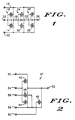
- a voltage detecting circuit 10 comprised primarily of a P-channel field effect transistor 12 and an N-channel field effect transistor 14.
- the transistor 12 has a P-type source region coupled to a positive supply voltage node 16, a P-type drain region coupled to a node 18, an N-type current channel region between the source and drain regions thereof and coupled to the positive supply voltage node 16, and a gate electrode adjacent to but insulated from the current channel region thereof and coupled to a negative supply voltage node 20.
- the transistor 14 has an N-type source region coupled to an input node 22, an N-type drain region coupled to the node 18, a P-type current channel region between the source and drain regions thereof and coupled to the input node 22, and a gate electrode adjacent to but insulated from the current channel region thereof and coupled to the negative supply voltage node 20.
- the positive and negative supply voltage nodes 16 and 20, respectively will be coupled to a power supply (not shown) capable of developing a potential differential of the order of +3 to +15 volts therebetween. Accordingly, the transistor 12 will be biased in the on or conducting condition, thereby tending to charge the node 18 toward the positive supply voltage. As long as the voltage on the input node 22 is within the range of the supply voltages, the transistor 14 will be biased in the off or non-conducting condition, thereby allowing the transistor 12 to charge node 18 to the positive supply voltage.
- the transistor 14 will be biased in the on or conducting condition, thereby tending to discharge the node 18 toward the voltage of the input signal. Under these conditions, the voltage on the node 18 will settle between the positive supply voltage and the voltage of the input signal, depending upon the relative saturation currents of the transistors 12 and 14.
- the on resistance of transistor 14 will be substantially smaller than the on resistance of transistor 12, so that the voltage drop across transistor 12 will be much greater than the drop across transistor 14 when the voltage of the input signal is sufficiently below the negative supply voltage to enable transistor 14 to conduct more current than transistor 12.
- the voltage on node 18 will be substantially equal to the voltage of the input signal.
- the grossly imbalanced source and sink currents on the node 18 in the above example may be undesirable.
- transistors 12 and 14 may be significantly smaller than in the example above, since the resulting increase in voltage on the node 18 is compensated for by including additional gain stages 24 and 26.
- the width to length ratios of transistors 12 and 14 may be 8/15 and 25/ 10, respectively, so that the resulting on resistance of transistor 14 will be still be smaller than the on resistance of transistor 12.
- the voltage on the node 18 will be in range of about -8 volts when the input signal is -15 volts.
- gain stage 24 which comprises a second P-channel field effect transistor 28 and a second N-channel field effect transistor 30 connected the same as the transistors 12 and 14, respectively, but with the gate electrodes thereof coupled to the node 18. If, for example, the width to length ratios of transistors 28 and 30 are selected to be 30/6 and 6/6, respectively, then the switch point of the gain stage 24 will be about 0 volts, and the voltage developed on node 32 will swing between the positive supply voltage and the voltage of the "design" input signal, i.e. -15 volts for the given example. It will be noted however, that the on resistance of the transistor 28 is still somewhat smaller than the on resistance of transistor 30.
- Gain stage 26 which comprises a third P-channel field effect transistor 34 and a third N-channel field effect transistor 36 connected the same as transistors 12 and 14, respectively, but with the gate electrodes coupled to the node 32.
- the switch point of the gain stage 26 will be half way between the positive supply voltage and the voltage of the "design" input signal, and the voltage developed on node 38 will swing between the positive supply voltage, i.e. +5 volts, and the voltage of the "design" input signal of-15 volts.
- the source and sink currents on node 38 will be the same.
- a voltage translating circuit 40 comprised of a P-channel field effect transistor 42 and three N-channel field effect transistors 44, 46 and 48.
- the transistor 42 has a P-type source region coupled to a positive supply voltage node 50, a P-type drain region coupled to an output node 52, an N-type current channel region between the source and drain regions thereof and coupled to the positive supply voltage node 50, and a gate electrode adjacent to but insulated from the current channel region thereof and coupled to a first input node 54.
- the transistor 44 has an N-type source region coupled to a second input node 56, an N-type drain region, a P-type current channel region between the source and drain regions thereof and coupled to the second input node 56, and a gate electrode adjacent to but insulated from the current channel region thereof and coupled to the first input node 54.
- the transistor 46 has an N-type source region coupled to the drain region of the transistor 44, an N-type drain region coupled to the output node 52, a P-type current channel region between the source and drain regions thereof and coupled to the second input node 56, and a gate electrode adjacent to but insulated from the current channel region thereof and coupled to a third input node 58.
- the transistor 48 has an N-type source region coupled to the second input node 56, an N-type drain region coupled to the output node 52, a P-type current channel region between the source and drain regions thereof and coupled to the second input node 56, and a gate electrode adjacent to but insulated from the current channel region thereof and coupled to a negative supply voltage node 60.
- the positive and negative supply voltage nodes 50 and 60 will be coupled to a power supply (not shown) capable of developing a potential differential of the order of +3 to +15 volts therebetween.
- the second input node 56 will be coupled to the negative supply voltage
- the third input node 58 will be coupled to the positive supply voltage.
- the transistor 46 will be biased in the on or conducting condition and the transistor 48 will be biased in the off or non-conducting condition.
- transistors 42 and 44 form an inverter with respect to the first input node 54, with transistor 42 charging output node 52 to the positive supply voltage in response to the first input node 54 being coupled to the negative supply voltage and transistor 44 discharging output node 52 to the negative supply voltage in response to the first input node 54 being coupled to the positive supply voltage.
- the second and third input nodes 56 and 58 will be coupled to a control voltage which is below the negative supply voltage by at least the threshold voltage of the transistors 44 and 48.
- the transistor 46 will be biased in the off or non-conducting condition and the transistor 48 will be biased in the on or conducting condition.
- transistors 42 and 48 form an inverterwith respect to the first input node 54, with transistor 42 being sufficiently strong to charge the output node 52 to the positive supply voltage in response to the first input node 54 being coupled to the negative supply voltage, and transistor 48 being allowed to discharge the output node 52 to the control voltage in response to the first input node 54 being coupled to the positive supply voltage to bias the transistor 42 in the off or non-conducting condition.
- the voltage detecting circuit 10 described above is in an electrically programmable read only memory (EPROM) integrated circuit to detect the coupling of a characteristic programming voltage outside the range of the normal supply voltages to a particular input pin, and thus enable the programming logic thereof.
- the voltage translating circuit 40 is suitable for cooperating with the voltage detecting circuit 10 to perform the word line select function. In this form, the voltage detecting circuit 10 selectively couples either the positive supply voltage or the programming voltage to the gate electrode of the transistor 46 depending upon whether or not the programming voltage is coupled to the second input node 56. In response, the voltage translating circuit 40 selectively couples the programming voltage from the second input node 56 to an associated array word line coupled to output node 52.
- the voltage detecting circuit 10 provides as the output thereof the positive supply voltage in the absence of an input signal having a voltage below the negative supply voltage, and the input signal itself when the latter is present.
- the voltage detecting circuit 10 can be easily used to detect an input signal above the positive supply voltage by coupling the negative supply voltage to node 22, the positive supply voltage to node 20, and the input signal to node 16.
- the output on node 38 will be the negative supply voltage in the absence of the input signal, and the input signal of +20 volts when the latter is present.
- either form of the voltage detecting circuit 10 may be made to respond to different "design" input signals outside the range of the selected positive and negative supply voltages by applying conventional algorithms to select the sizes of transistors 12 and 14, and, if present, transistors 26-28 and 34-36.
- the voltage translating circuit 40 provides as the output thereof the positive or negative supply voltages selected via the signal applied to the first input node 54 when the signal applied to the second and third input nodes 56 and 58, respectively, are not below the negative supply voltage; and between the positive supply voltage and the voltage on the second and third input nodes 56 and 58, respectively, when the latter is below the negative supply voltage.
- the voltage translating circuit 40 can be easily modified to translate to voltages above the positive supply voltage.
Landscapes
- Engineering & Computer Science (AREA)
- Power Engineering (AREA)
- Physics & Mathematics (AREA)
- Computer Hardware Design (AREA)
- Computing Systems (AREA)
- General Engineering & Computer Science (AREA)
- Mathematical Physics (AREA)
- Measurement Of Current Or Voltage (AREA)
Abstract
Claims (5)
Applications Claiming Priority (4)
| Application Number | Priority Date | Filing Date | Title |
|---|---|---|---|
| US06/395,424 US4521696A (en) | 1982-07-06 | 1982-07-06 | Voltage detecting circuit |
| US395424 | 1982-07-06 | ||
| US06/395,958 US4469960A (en) | 1982-07-07 | 1982-07-07 | Voltage translating circuit |
| US395958 | 1982-07-07 |
Publications (3)
| Publication Number | Publication Date |
|---|---|
| EP0112895A1 EP0112895A1 (fr) | 1984-07-11 |
| EP0112895A4 EP0112895A4 (fr) | 1984-09-11 |
| EP0112895B1 true EP0112895B1 (fr) | 1988-02-03 |
Family
ID=27015104
Family Applications (1)
| Application Number | Title | Priority Date | Filing Date |
|---|---|---|---|
| EP19830902349 Expired EP0112895B1 (fr) | 1982-07-06 | 1983-06-08 | Circuit de detection et de transformation de tension |
Country Status (4)
| Country | Link |
|---|---|
| EP (1) | EP0112895B1 (fr) |
| DE (1) | DE3375627D1 (fr) |
| HK (1) | HK46990A (fr) |
| WO (1) | WO1984000453A1 (fr) |
Family Cites Families (9)
| Publication number | Priority date | Publication date | Assignee | Title |
|---|---|---|---|---|
| US3936676A (en) * | 1974-05-16 | 1976-02-03 | Hitachi, Ltd. | Multi-level voltage supply circuit for liquid crystal display device |
| US4322639A (en) * | 1976-08-26 | 1982-03-30 | Hitachi, Ltd. | Voltage detection circuit |
| US4045688A (en) * | 1976-10-26 | 1977-08-30 | Rca Corporation | Power-on reset circuit |
| US4064405A (en) * | 1976-11-09 | 1977-12-20 | Westinghouse Electric Corporation | Complementary MOS logic circuit |
| JPS55149871A (en) * | 1978-07-31 | 1980-11-21 | Fujitsu Ltd | Line voltage detector |
| DE2840006C2 (de) * | 1978-09-14 | 1980-10-02 | Deutsche Itt Industries Gmbh, 7800 Freiburg | CMOS-Schaltung zur Umwandlung eines Ternärsignals in zwei Binärsignale und Verwendung dieser CMOS-Schaltung |
| GB2065404B (en) * | 1979-12-11 | 1984-05-31 | Casio Computer Co Ltd | Voltage selector circuit |
| US4270190A (en) * | 1979-12-27 | 1981-05-26 | Rca Corporation | Small signal memory system with reference signal |
| US4348596A (en) * | 1979-12-27 | 1982-09-07 | Rca Corporation | Signal comparison circuit |
-
1983
- 1983-06-08 EP EP19830902349 patent/EP0112895B1/fr not_active Expired
- 1983-06-08 WO PCT/US1983/000905 patent/WO1984000453A1/fr not_active Ceased
- 1983-06-08 DE DE8383902349T patent/DE3375627D1/de not_active Expired
-
1990
- 1990-06-14 HK HK46990A patent/HK46990A/en not_active IP Right Cessation
Also Published As
| Publication number | Publication date |
|---|---|
| HK46990A (en) | 1990-06-22 |
| EP0112895A4 (fr) | 1984-09-11 |
| WO1984000453A1 (fr) | 1984-02-02 |
| DE3375627D1 (en) | 1988-03-10 |
| EP0112895A1 (fr) | 1984-07-11 |
Similar Documents
| Publication | Publication Date | Title |
|---|---|---|
| EP0121217B1 (fr) | Circuit tampon de sortie | |
| US5042011A (en) | Sense amplifier pulldown device with tailored edge input | |
| US5646503A (en) | Method for balancing power sources and structure therefor | |
| US4725981A (en) | Random access memory cell resistant to inadvertant change of state due to charged particles | |
| US4749880A (en) | Circuit for detecting level of input voltage | |
| JP2816727B2 (ja) | シングルエンデッドセンス増幅器 | |
| US5208488A (en) | Potential detecting circuit | |
| KR900000993B1 (ko) | 개선된 출력특성을 갖는 비교기 회로 | |
| US5367491A (en) | Apparatus for automatically initiating a stress mode of a semiconductor memory device | |
| JPH0160789B2 (fr) | ||
| US4542306A (en) | Buffer circuits for use with semiconductor memory devices | |
| US4521696A (en) | Voltage detecting circuit | |
| US4728820A (en) | Logic state transition detection circuit for CMOS devices | |
| US4048518A (en) | MOS buffer circuit | |
| US5161123A (en) | Semiconductor memory | |
| US3976895A (en) | Low power detector circuit | |
| JPS6237470B2 (fr) | ||
| US4594518A (en) | Voltage level sensing circuit | |
| US5834953A (en) | High speed current sense amplifier | |
| US4464590A (en) | Memory system current sense amplifier circuit | |
| US4709352A (en) | MOS read-only memory systems | |
| US4469960A (en) | Voltage translating circuit | |
| US5345111A (en) | High-speed current sense amplifier | |
| US5175705A (en) | Semiconductor memory device having circuit for prevention of overcharge of column line | |
| HK46990A (en) | A voltage detecting and translating circuit |
Legal Events
| Date | Code | Title | Description |
|---|---|---|---|
| PUAI | Public reference made under article 153(3) epc to a published international application that has entered the european phase |
Free format text: ORIGINAL CODE: 0009012 |
|
| 17P | Request for examination filed |
Effective date: 19840309 |
|
| AK | Designated contracting states |
Designated state(s): DE FR GB NL |
|
| GRAA | (expected) grant |
Free format text: ORIGINAL CODE: 0009210 |
|
| AK | Designated contracting states |
Kind code of ref document: B1 Designated state(s): DE FR GB NL |
|
| REF | Corresponds to: |
Ref document number: 3375627 Country of ref document: DE Date of ref document: 19880310 |
|
| ET | Fr: translation filed | ||
| PLBE | No opposition filed within time limit |
Free format text: ORIGINAL CODE: 0009261 |
|
| STAA | Information on the status of an ep patent application or granted ep patent |
Free format text: STATUS: NO OPPOSITION FILED WITHIN TIME LIMIT |
|
| 26N | No opposition filed | ||
| PGFP | Annual fee paid to national office [announced via postgrant information from national office to epo] |
Ref country code: GB Payment date: 19980401 Year of fee payment: 16 |
|
| PGFP | Annual fee paid to national office [announced via postgrant information from national office to epo] |
Ref country code: FR Payment date: 19980407 Year of fee payment: 16 |
|
| PGFP | Annual fee paid to national office [announced via postgrant information from national office to epo] |
Ref country code: NL Payment date: 19980420 Year of fee payment: 16 |
|
| PGFP | Annual fee paid to national office [announced via postgrant information from national office to epo] |
Ref country code: DE Payment date: 19980423 Year of fee payment: 16 |
|
| PG25 | Lapsed in a contracting state [announced via postgrant information from national office to epo] |
Ref country code: GB Free format text: LAPSE BECAUSE OF NON-PAYMENT OF DUE FEES Effective date: 19990608 |
|
| PG25 | Lapsed in a contracting state [announced via postgrant information from national office to epo] |
Ref country code: FR Free format text: THE PATENT HAS BEEN ANNULLED BY A DECISION OF A NATIONAL AUTHORITY Effective date: 19990630 |
|
| PG25 | Lapsed in a contracting state [announced via postgrant information from national office to epo] |
Ref country code: NL Free format text: LAPSE BECAUSE OF NON-PAYMENT OF DUE FEES Effective date: 20000101 |
|
| GBPC | Gb: european patent ceased through non-payment of renewal fee |
Effective date: 19990608 |
|
| NLV4 | Nl: lapsed or anulled due to non-payment of the annual fee |
Effective date: 20000101 |
|
| PG25 | Lapsed in a contracting state [announced via postgrant information from national office to epo] |
Ref country code: DE Free format text: LAPSE BECAUSE OF NON-PAYMENT OF DUE FEES Effective date: 20000503 |
|
| REG | Reference to a national code |
Ref country code: FR Ref legal event code: ST |