EP0121217B1 - Circuit tampon de sortie - Google Patents
Circuit tampon de sortie Download PDFInfo
- Publication number
- EP0121217B1 EP0121217B1 EP84103372A EP84103372A EP0121217B1 EP 0121217 B1 EP0121217 B1 EP 0121217B1 EP 84103372 A EP84103372 A EP 84103372A EP 84103372 A EP84103372 A EP 84103372A EP 0121217 B1 EP0121217 B1 EP 0121217B1
- Authority
- EP
- European Patent Office
- Prior art keywords
- level
- data
- circuit
- vdd
- output terminal
- Prior art date
- Legal status (The legal status is an assumption and is not a legal conclusion. Google has not performed a legal analysis and makes no representation as to the accuracy of the status listed.)
- Expired
Links
- 230000004044 response Effects 0.000 claims description 12
- 230000000694 effects Effects 0.000 claims description 5
- 238000007599 discharging Methods 0.000 claims description 2
- 230000002401 inhibitory effect Effects 0.000 claims 3
- 230000007704 transition Effects 0.000 description 31
- 239000003990 capacitor Substances 0.000 description 19
- 239000004065 semiconductor Substances 0.000 description 7
- 239000012535 impurity Substances 0.000 description 4
- 238000010586 diagram Methods 0.000 description 3
- 238000009413 insulation Methods 0.000 description 2
- 238000005468 ion implantation Methods 0.000 description 2
- 239000000758 substrate Substances 0.000 description 2
- 230000003247 decreasing effect Effects 0.000 description 1
- 238000001514 detection method Methods 0.000 description 1
- 230000004048 modification Effects 0.000 description 1
- 238000012986 modification Methods 0.000 description 1
- 238000004904 shortening Methods 0.000 description 1
Images

Classifications
-
- G—PHYSICS
- G11—INFORMATION STORAGE
- G11C—STATIC STORES
- G11C7/00—Arrangements for writing information into, or reading information out from, a digital store
- G11C7/10—Input/output [I/O] data interface arrangements, e.g. I/O data control circuits, I/O data buffers
- G11C7/1051—Data output circuits, e.g. read-out amplifiers, data output buffers, data output registers, data output level conversion circuits
- G11C7/1057—Data output buffers, e.g. comprising level conversion circuits, circuits for adapting load
-
- G—PHYSICS
- G11—INFORMATION STORAGE
- G11C—STATIC STORES
- G11C7/00—Arrangements for writing information into, or reading information out from, a digital store
- G11C7/10—Input/output [I/O] data interface arrangements, e.g. I/O data control circuits, I/O data buffers
- G11C7/1051—Data output circuits, e.g. read-out amplifiers, data output buffers, data output registers, data output level conversion circuits
-
- G—PHYSICS
- G11—INFORMATION STORAGE
- G11C—STATIC STORES
- G11C7/00—Arrangements for writing information into, or reading information out from, a digital store
- G11C7/10—Input/output [I/O] data interface arrangements, e.g. I/O data control circuits, I/O data buffers
- G11C7/1051—Data output circuits, e.g. read-out amplifiers, data output buffers, data output registers, data output level conversion circuits
- G11C7/106—Data output latches
-
- H—ELECTRICITY
- H03—ELECTRONIC CIRCUITRY
- H03K—PULSE TECHNIQUE
- H03K19/00—Logic circuits, i.e. having at least two inputs acting on one output; Inverting circuits
- H03K19/01—Modifications for accelerating switching
- H03K19/017—Modifications for accelerating switching in field-effect transistor circuits
- H03K19/01707—Modifications for accelerating switching in field-effect transistor circuits in asynchronous circuits
-
- H—ELECTRICITY
- H03—ELECTRONIC CIRCUITRY
- H03K—PULSE TECHNIQUE
- H03K19/00—Logic circuits, i.e. having at least two inputs acting on one output; Inverting circuits
- H03K19/01—Modifications for accelerating switching
- H03K19/017—Modifications for accelerating switching in field-effect transistor circuits
- H03K19/01707—Modifications for accelerating switching in field-effect transistor circuits in asynchronous circuits
- H03K19/01721—Modifications for accelerating switching in field-effect transistor circuits in asynchronous circuits by means of a pull-up or down element
Definitions
- the present invention relates to an output buffer circuit for a high-speed semiconductor logic device such as a semiconductor memory and a microprocessor and, more particularly to an output buffer circuit for generating output data in response to signal representing that input data will be supplied thereto after a predetermined time has passed.
- Fig. 1 is a conventional output buffer circuit for a semiconductor memory.
- This output buffer circuit has a data input terminal IN connected to output terminals of a plurality of memory cells (not shown) through a bit line, a control terminal (p which receives a signal for disabling a data output, load and drive transistors 10 and 12, and a driver 14 for controlling the conduction states of the transistors 10 and 12 in accordance with a logic value of data supplied through the terminal IN.
- the driver 14 is operated to render the transistors 10 and 12 nonconductive while the disable signal is supplied from the terminal q ).
- a data output terminal OUT of the output buffer circuit is connected through a current path of the transistor 10 to a power source terminal VD to which a voltage VDD (e.g., 5 V) is supplied and which is grounded through a current path of the transistor 12.
- VDD voltage
- a capacitor 16 used as a load is connected to the data output terminal OUT.
- the capacitor 16 has a large capacitance.
- the address signal is changed to read out the data of "0" from the second memory cell.
- the data of logic value "0" is supplied from the second memory cell to the output buffer circuit after a predetermined period of time, the transistors 10 and 12 are respectively rendered nonconductive and conductive. Therefore, a discharge current flows from the capacitor 16, so that the voltage of the data output terminal OUT is decreased to the ground potential level, as shown in Fig. 2(B).
- This precharge circuit is used to set the potential of a bitline at VDD/2 prior to writing of data into a memory cell or reading of data out of the memory cell.
- VDD/2 of the bitline is not equal to the transition point of each inverter included in the memory cell and a sense amplifier, the inverter cannot sense the data transferred through the bitline quickly. That is, the potential of the bitline is set equal to the transition point of the inverters so that the inverter can sense the data from a slight potential change of the bitline.
- the precharge circuit uses p- and n-channel transistors connected so that the potential of the bitline connected to a mode between these transistors is determined by the ratio of ON resistances of the p- and n-channel transistors. Therefore, currents flow through these transistors, even if the potential of the bitline has been set at VDD/2.
- prior art document GB-A-2070372 describes a semiconducor memory device which comprises data lines each connected with memory cells, a precharging circuit for precharging the data lines, and an address signal state transition detector to detect a state transition of an address signal to cause the precharging circuit to precharge the data lines.
- a data line voltage level detector detects the voltage level of data lines being precharged to minimize the precharging period of the data lines, and a flipflop causes the precharging circuit to precharge the data lines when an address signal state transition is detected by the address signal state transition detector.
- the flipflops disables the precharging circuit from precharging the data lines when the voltage level detector detects that the data lines have been precharged to a predetermined voltage level.
- the present invention provides an output buffer circuit as stated in claim 1.
- Fig. 3 shows an output buffer circuit for a semiconductor memory according to an embodiment of the present invention.
- the output buffer circuit has n- and p-channel MOS transistors 20 and 22 and a driver 24 for selectively turning on the transistors 20 and 22 in accordance with a logic value of data supplied thereto through a data input terminal IN, as shown in Fig. 3.
- An output terminal OUT of the output buffer circuit is connected through a current path of the transistor 20 to a power source terminal VD to which a voltage VDD (e.g., 5 V) is supplied, and is grounded through a current path of the transistor 22.
- VDD voltage
- One end of a capacitor 26 serving as a load is connected to the data output terminal OUT, and the other end thereof is grounded.
- the driver 24 includes a latch section and a selector section.
- the latch section has inverters 28 and 30.
- the selector section has a 2-input NOR gate 32, a 2-input NAND gate 34, and inverters 36, 38 and 40.
- the input terminal of the inverter 28 is connected to the data input terminal IN and the output terminal of the inverter 30.
- the output terminal of the inverter 28 is connected to the input terminal of the inverter 30, the first input terminal of the NOR gate 32, and the first input terminal of the NAND gate 34.
- the output terminal of the NOR gate 32 is connected to the gate of the p-channel MOS transistor 20 through the inverter 36.
- the output terminal of the NAND gate 34 is connected to the gate of the n-channel MOS transistor 22 through the inverter 38.
- the input terminal IN is connected to the output terminals of memory cells 42-1, 42-2, ..., and 42-M through a bit line BL.
- Address signals A1, A2,..., and AN are supplied to a decoder 44 for specifying read access of one of the memory cells 421, 422, . . ., and 42-M in response to the address signals A1, A2, ..., and AN.
- the output buffer circuit further comprises a transition detector circuit 46 for detecting a change in address signals A1 to AN and generating a pulse signal which is set at high level (i.e., VDD) for a predetermined period of time, and a preset circuit 48 for presetting a potential at the data output terminal OUT to be an intermediate potential (i.e., VDD/2) of the power source voltage VDD in response to the pulse signal generated from the transition detector circuit 46.
- the preset circuit 48 has an n-channel MOS transistor 50 whose gate is directly connected to the output terminal of the transition detector circuit 46, and a p-channel MOS transistor 52 whose gate is connected to the output terminal of the transition detector circuit 46 through an inverter 54.
- the current path of the transistor 50 is connected between the data output terminal OUT and the power source terminal VD.
- the data output terminal OUT is grounded through the current path of the transistor 52.
- the transition detector circuit 46 comprises N one-bit transition detectors which respond to the respective address signals A1, A2, ..., and AN.
- One of the 1-bit transition detectors is illustrated in Fig. 4.
- a pulse signal from each 1-bit transition detector is supplied to the preset circuit 48 through an OR gate (not shown). This pulse signal is also supplied to the second input terminal of the NAND gate 34 through the inverter 40 and directly to the second input terminal of the NOR gate 32.
- the transition detector shown in Fig. 4 has an exclusive OR gate 56 and inverters 58 to 61 constituting a delay circuit.
- One of the address signals A1 to AN is directly supplied to the first input terminal of the exclusive OR gate 56 and to a second input terminal thereof through a series circuit of the inverters 58 to 61.
- the address signals A1 to AN are updated.
- the decoder 44 permits the reading operation of the memory cell 42-1, and the transition detector circuit 46 generates a pulse signal (e.g., VDD level) of a predetermined pulse width, for example, corresponding to the delay time of the inverters 58 to 61.
- the driver makes the transistors 20 and 22 nonconductive when receiving the pulse signal. In this case, when the capacitor 26 is not charged, the potential of the data output terminal OUT is at ground level.
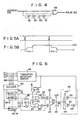
- the preset circuit 48 changes the potential of the data output terminal OUT to an intermediate level (i.e., VDD/2) of the power source voltage VDD in response to the pulse signal as shown in Fig. 5B.
- VDD/2 intermediate level
- This operation is completed before the readout data from the memory cell 42-1 is sent on the bit line BL.
- this data is supplied to the input terminal IN and is latched by the latch section of inverters 28 and 30.
- the selector section of the driver 24 renders the transistors 20 and 22 conductive and nonconductive, respectively, in accordance with the logic value "1" of the data from the latch section. Therefore, a charge current is supplied to the capacitor 26 through the transistor 20, so that the potential at the data output terminal OUT is increased from the VDD/2 level to the VDD level, as shown in Fig. 5B.
- the potential at the terminal OUT is changed from the VDD level to the VDD/2 level.
- data of logic level "0" is read out from the memory cell 42-2 onto the bit line BL.
- This data is supplied to the input terminal IN of the output buffer circuit and is latched by the latch section of the inverters 28 and 30 in the driver 24.
- the selector section of the driver 24 makes the transistors 20 and 22 nonconductive and conductive, respectively, in accordance with the logic value "0" of the data from the latch section.
- the discharge current is supplied to the capacitor 26 through the transistor 22, so that the potential at the data output terminal OUT changes from the VDD/2 level to the ground level (i.e., 0 V), as shown in Fig. 5B.
- the preset circuit 48 will be described more in detail.
- the sources of the n- and p-channel MOS transistors 50 and 52 are commonly connected to the data output terminal OUT and serve as a common output terminal of the preset circuit 48.
- a threshold voltage of the MOS transistors 50 and 52 changes in accordance with a change in a source voltage (i.e., a change in voltage at the terminal OUT) due to a back gate biasing effect.
- the transition detector circuit 46 generates a low level signal (ground level) except for the case wherein the address signals A1 to AN are updated. In this case, the transistors 50 and 52 are held nonconductive.
- the transition detector circuit 46 When the transition detector circuit 46 generates a high level signal (VDD level) as a pulse signal, one of the MOS transistors 50 and 52 is selectively turned on, and the other is turned off.
- the transistor 50 is turned on during a period while the voltage VOUT at the data output terminal OUT is lower than the VDD/2 level, so that a charge current flows to the capacitor 26. Accordingly, the voltage VOUT at the terminal OUT rises to the VDD/2 level.
- the transistor 52 is turned on for a period while the output voltage VOUT at the data output terminal OUT is higher than the VDD/2 level, so that the discharge current flows from the capacitor 26.
- the voltage VOUT at the data output terminal OUT changes from the VDD level to the VDD/2 level.
- the transistors 50 and 52 are both rendered nonconductive.
- This operation can be accomplished when the n- and p-channel MOS transistors 50 and 52 satisfy a specific condition given by a mathematical analysis.
- a threshold voltage VP ( ⁇ 0 V) of the MOS transistor 52 is given as follows:
- the transition detector 46 is generating the high level signal (VDD level)
- the gate-source voltage of the MOS transistor 50 set to be VDD-VOUT.
- the conduction condition of the MOS transistor 50 is given as follows:
- the nonconduction condition of the MOS transistor 50 is given s follows:
- the capacitor 26 receives the charge current through the MOS transistor 50 so as to raise the potential VOUT at the data output terminal OUT to VM1 level.
- the VM1 level is the voltage VOUT at the terminal OUT when equality is established in inequality (3) and is given as follows: If the voltage VM1 satisfies inequality (6), the MOS transistor 52 is held nonconductive until the voltage VOUT at the data output terminal OUT reaches the VM1 level. In this case, the MOS transistor 52 does not influence an increase in voltage VOUT at the data output terminal.
- inequality (8) can be rewritten as follows: Now assume that the voltage VOUT at the data output terminal OUT is set at the VDD level. Inequality (4) is satisifed so that the MOS transistor 50 is rendered nonconductive. At the same time, inequality (5) is satisfied so that the MOS transistor is rendered conductive.
- the capacitor 26 then receives the discharge current through the MOS transistor 52, so that the potential VOUT at the data output terminal falls to a VM2 level given as follows:
- the condition for holding the MOS transistor 50 in the nonconductive state until the potential VOUT reaches the VM2 level is given as follows:
- the condition for holding the MOS transistor 50 in the nonconductive state while the MOS transistor 52 is held conductive is given as follows:
- the right-hand side of inequality (12) corresponds to VM1, so that inequality (12) can be rewritten as follows:
- inequalities (9) and (13) are simultaneously established, the following equation is established:
- the MOS transistors 50 and 52 are respectively rendered nonconductive and conductive while the voltage VOUT at the data output terminal OUT changes from the VDD level to the VM level (i.e., VDD/2).
- the MOS transistors 50 and 52 are respectively rendered conductive and nonconductive while the voltage VOUT changes from the ground level to the VM level (i.e., VDD/2).
- the preset circuit 48 sets a voltage at the data output terminal OUT to be an intermediate potential VM between the power source voltage VDD and the ground level while the transition detector circuit 46 generates the pulse signal in response to updating of the address signals A1 to AN.
- each of KP and KN is given in accordance with the impurity concentration in the channel region of the p-channel and n-channel MOS transistors. The impurity concentration is determined by the ion-implantation condition in the channel region. Therefore, the n- and p-channel MOS transistors 50 and 52 are formed under the ion-implantation condition of the channel such that KN and KP satisfy equation (15).
- a change in level of each of the address signals A1 to AN is detected by the transition detector circuit 46, so that the capacitor 26 can be charged or discharged prior to reception of readout data from the memory cell, thereby presetting the voltage at the data output terminal OUT to be the VDD/2 level. For this reason, the memory access time TD can, therefore, be shortened. In particular, if the capacitance of the capacitor 26 is large, this effect of shortening the time TD can be emphasized.
- One of the n- and p-channel MOS transistors 50 and 52 is rendered conductive in response to the signal generated from the transition detection circuit 46 so as to shift the voltage VOUT at the data output terminal OUT to the VDD/2 level.
- the MOS transistors 50 and 52 are simultaneously rendered nonconductive, resulting in low power consumption.
- transistors 20 and 22 are rendered nonconductive while a preset circuit 48 supplies a charge or discharge current to a capacitor 26. For this reason, a short-circuit current will not flow in the ground terminal from the terminal VD through the transistors 50 and 22 or transistors 20 and 52. If this short-circuit current is present, power consumption increases, and charging and discharging of the capacitor 26 is prevented.
- Fig. 6 shows an output buffer circuit according to another embodiment of the present invention.
- the same reference numerals used in Fig. 6 denote the same parts as in Fig. 3, and a detailed description thereof will be omitted.
- This output buffer circuit further comprises a 2-input OR gate 63.
- the first input terminal of the OR gate 63 is connected to a control terminal q) to which a control signal is supplied, and the second terminal thereof is connected to the output terminal of a transition detector circuit 46.
- the output terminal of the OR gate 63 is directly connected to the second input terminal of a NOR gate 32 and to the second input terminal of a NAND gate 34 through an inverter 40.
- the driver 24 makes the transistors 20, 22 nonconductive in response to one of the signals from the terminaI ⁇ and the transition detector circuit 46. Therefore, it is possible to interrupt the buffer operation of the output buffer circuit, for example, while the memory cells 42-1 to 42-M is in a writing mode.
- the output voltage can be charged at a high speed in accordance with the logic value of the supplied data, and power consumption can be reduced.
- the output buffer circuit is not limited to an application for an output of data read out from the semiconductor memory.
- the transition detector circuit 46 may be connected to receive, instead of the address signals, a signal which simply represents that data will be supplied to the data input terminal IN after a predetermined period of time.
- the p- and n-channel MOS transistors 20 and 22 may be formed of MOS transistors of the same channel.
- the driver 24 need not have the latch section.
Landscapes
- Physics & Mathematics (AREA)
- Engineering & Computer Science (AREA)
- Computer Hardware Design (AREA)
- Computing Systems (AREA)
- General Engineering & Computer Science (AREA)
- Mathematical Physics (AREA)
- Logic Circuits (AREA)
- Static Random-Access Memory (AREA)
Claims (6)


Applications Claiming Priority (2)
| Application Number | Priority Date | Filing Date | Title |
|---|---|---|---|
| JP56028/83 | 1983-03-31 | ||
| JP58056028A JPS59181829A (ja) | 1983-03-31 | 1983-03-31 | 半導体素子の出力バツフア回路 |
Publications (3)
| Publication Number | Publication Date |
|---|---|
| EP0121217A2 EP0121217A2 (fr) | 1984-10-10 |
| EP0121217A3 EP0121217A3 (en) | 1987-01-28 |
| EP0121217B1 true EP0121217B1 (fr) | 1990-12-27 |
Family
ID=13015607
Family Applications (1)
| Application Number | Title | Priority Date | Filing Date |
|---|---|---|---|
| EP84103372A Expired EP0121217B1 (fr) | 1983-03-31 | 1984-03-27 | Circuit tampon de sortie |
Country Status (4)
| Country | Link |
|---|---|
| US (1) | US4570091A (fr) |
| EP (1) | EP0121217B1 (fr) |
| JP (1) | JPS59181829A (fr) |
| DE (1) | DE3483842D1 (fr) |
Families Citing this family (39)
| Publication number | Priority date | Publication date | Assignee | Title |
|---|---|---|---|---|
| US4687954A (en) * | 1984-03-06 | 1987-08-18 | Kabushiki Kaisha Toshiba | CMOS hysteresis circuit with enable switch or natural transistor |
| US4710648A (en) * | 1984-05-09 | 1987-12-01 | Hitachi, Ltd. | Semiconductor including signal processor and transient detector for low temperature operation |
| EP0194939B1 (fr) * | 1985-03-14 | 1992-02-05 | Fujitsu Limited | Dispositif de mémoire semi-conducteur |
| JPS6214520A (ja) * | 1985-07-12 | 1987-01-23 | Sony Corp | メモリの出力バツフア回路 |
| JPH0720060B2 (ja) * | 1985-08-14 | 1995-03-06 | 株式会社東芝 | 出力回路装置 |
| JPS62167698A (ja) * | 1986-01-20 | 1987-07-24 | Fujitsu Ltd | 半導体記億装置 |
| US4692635A (en) * | 1986-06-26 | 1987-09-08 | National Semiconductor Corp. | Self-timed logic level transition detector |
| JPS63112893A (ja) * | 1986-10-28 | 1988-05-17 | Mitsubishi Electric Corp | 半導体集積回路 |
| FR2614743A1 (fr) * | 1987-04-29 | 1988-11-04 | Matra Harris Semiconducteurs | Circuit integre numerique a prechargement |
| US4806794A (en) * | 1987-07-22 | 1989-02-21 | Advanced Micro Devices, Inc. | Fast, low-noise CMOS output buffer |
| US4882507B1 (en) * | 1987-07-31 | 1993-03-16 | Output circuit of semiconductor integrated circuit device | |
| JPH0817037B2 (ja) * | 1987-12-03 | 1996-02-21 | 松下電子工業株式会社 | スタティックramの出力回路 |
| US4959816A (en) * | 1987-12-28 | 1990-09-25 | Kabushiki Kaisha Toshiba | Semiconductor integrated circuit |
| KR910002748B1 (ko) * | 1988-04-12 | 1991-05-04 | 삼성 반도체통신 주식회사 | 반도체장치에 있어서 데이타 출력 버퍼회로 |
| US4851720A (en) * | 1988-09-02 | 1989-07-25 | Cypress Semiconductor Corporation | Low power sense amplifier for programmable logic device |
| US4965474A (en) * | 1988-09-16 | 1990-10-23 | Texas Instruments Incorporated | Glitch suppression circuit |
| JP2754603B2 (ja) * | 1988-10-14 | 1998-05-20 | 日本電気株式会社 | メモリデータ出力回路 |
| US5036223A (en) * | 1989-05-22 | 1991-07-30 | Kabushiki Kaisha Toshiba | Inverter circuit and chopper type comparator circuit using the same |
| KR920000962B1 (ko) * | 1989-05-26 | 1992-01-31 | 삼성전자 주식회사 | 반도체 메모리 장치의 데이터 출력단 전압레벨 조절회로 |
| KR910005602B1 (ko) * | 1989-06-15 | 1991-07-31 | 삼성전자 주식회사 | 어드레스 변환 검출에 따른 출력버퍼의 프리챠아지 제어방법 |
| JPH03219495A (ja) * | 1990-01-24 | 1991-09-26 | Sony Corp | 出力回路 |
| JPH03268298A (ja) * | 1990-03-16 | 1991-11-28 | Fujitsu Ltd | 半導体集積回路装置 |
| IT1240012B (it) * | 1990-04-27 | 1993-11-27 | St Microelectronics Srl | Stadio d'uscita dati, del tipo cosiddetto buffer,a ridotto rumore verso massa per circuiti logici di tipo cmos |
| US5241221A (en) * | 1990-07-06 | 1993-08-31 | North American Philips Corp., Signetics Div. | CMOS driver circuit having reduced switching noise |
| JP2900559B2 (ja) * | 1990-08-09 | 1999-06-02 | 日本電気株式会社 | データ出力回路 |
| JPH04150224A (ja) * | 1990-10-15 | 1992-05-22 | Internatl Business Mach Corp <Ibm> | 集積回路 |
| JP2690624B2 (ja) * | 1991-01-30 | 1997-12-10 | 日本電気株式会社 | バッファ回路 |
| KR940010838B1 (ko) * | 1991-10-28 | 1994-11-17 | 삼성전자 주식회사 | 데이타 출력 콘트롤 회로 |
| US5331228A (en) * | 1992-07-31 | 1994-07-19 | Sgs-Thomson Microelectronics, Inc. | Output driver circuit |
| JP2599196Y2 (ja) * | 1992-09-14 | 1999-08-30 | 本田技研工業株式会社 | 車両のエンジンマウント |
| KR960006911B1 (ko) * | 1992-12-31 | 1996-05-25 | 현대전자산업주식회사 | 데이타 출력버퍼 |
| US5423030A (en) * | 1993-09-13 | 1995-06-06 | Unisys Corporation | Bus station abort detection |
| DE4441523C1 (de) * | 1994-11-22 | 1996-05-15 | Itt Ind Gmbh Deutsche | Digitale Treiberschaltung für eine integrierte Schaltung |
| JP2743878B2 (ja) * | 1995-08-30 | 1998-04-22 | 日本電気株式会社 | 入力バッファ回路 |
| US5633603A (en) * | 1995-12-26 | 1997-05-27 | Hyundai Electronics Industries Co., Ltd. | Data output buffer using pass transistors biased with a reference voltage and a precharged data input |
| US5867038A (en) * | 1996-12-20 | 1999-02-02 | International Business Machines Corporation | Self-timed low power ratio-logic system having an input sensing circuit |
| ITTO20010531A1 (it) * | 2001-06-01 | 2002-12-01 | St Microelectronics Srl | Buffer di uscita per una memoria non volatile con controllo dello slew rate ottimizzato. |
| GB2388981B (en) * | 2002-05-20 | 2006-11-15 | Micron Technology Inc | Increasing drive strength and reducing propagation delays through the use of feedback |
| US7741879B2 (en) * | 2007-02-22 | 2010-06-22 | Avago Technologies Enterprise IP (Singapore) Pte. Ltd. | Apparatus and method for generating a constant logical value in an integrated circuit |
Family Cites Families (8)
| Publication number | Priority date | Publication date | Assignee | Title |
|---|---|---|---|---|
| US3909631A (en) * | 1973-08-02 | 1975-09-30 | Texas Instruments Inc | Pre-charge voltage generating system |
| US3937988A (en) * | 1974-04-05 | 1976-02-10 | Fairchild Camera And Instrument Corporation | Active termination network for clamping a line signal |
| US3935476A (en) * | 1974-12-13 | 1976-01-27 | Mostek Corporation | Combination output/input logic for integrated circuit |
| US4208730A (en) * | 1978-08-07 | 1980-06-17 | Rca Corporation | Precharge circuit for memory array |
| GB2070372B (en) * | 1980-01-31 | 1983-09-28 | Tokyo Shibaura Electric Co | Semiconductor memory device |
| US4498021A (en) * | 1982-07-13 | 1985-02-05 | Matsushita Electric Industrial Co., Ltd. | Booster for transmitting digital signal |
| US4465945A (en) * | 1982-09-03 | 1984-08-14 | Lsi Logic Corporation | Tri-state CMOS driver having reduced gate delay |
| US4488066A (en) * | 1982-11-08 | 1984-12-11 | At&T Bell Laboratories | Databus coupling arrangement using transistors of complementary conductivity type |
-
1983
- 1983-03-31 JP JP58056028A patent/JPS59181829A/ja active Pending
-
1984
- 1984-03-23 US US06/592,717 patent/US4570091A/en not_active Expired - Lifetime
- 1984-03-27 DE DE8484103372T patent/DE3483842D1/de not_active Expired - Lifetime
- 1984-03-27 EP EP84103372A patent/EP0121217B1/fr not_active Expired
Also Published As
| Publication number | Publication date |
|---|---|
| DE3483842D1 (de) | 1991-02-07 |
| US4570091A (en) | 1986-02-11 |
| JPS59181829A (ja) | 1984-10-16 |
| EP0121217A3 (en) | 1987-01-28 |
| EP0121217A2 (fr) | 1984-10-10 |
Similar Documents
| Publication | Publication Date | Title |
|---|---|---|
| EP0121217B1 (fr) | Circuit tampon de sortie | |
| US4389705A (en) | Semiconductor memory circuit with depletion data transfer transistor | |
| US6191978B1 (en) | Non-volatile semiconductor memory device | |
| US4908795A (en) | Semiconductor integrated circuit device with built-in memories | |
| US6181591B1 (en) | High speed CAM cell | |
| EP0337393B1 (fr) | EPROM du type à 2-cellules par bit | |
| KR950014093B1 (ko) | 반도체 메모리장치 | |
| US5297092A (en) | Sense amp for bit line sensing and data latching | |
| US4692902A (en) | Semiconductor read only memory device with improved access time | |
| US5777935A (en) | Memory device with fast write recovery and related write recovery method | |
| US5619149A (en) | Single ended dynamic sense amplifier | |
| JP2816727B2 (ja) | シングルエンデッドセンス増幅器 | |
| US5293345A (en) | Semiconductor memory device having a data detection circuit with two reference potentials | |
| KR920000838B1 (ko) | 프로그램이 가능한 논리 어레이 회로 | |
| JPH06162776A (ja) | 半導体メモリ回路 | |
| US4130897A (en) | MNOS FET memory retention characterization test circuit with enhanced sensitivity and power conservation | |
| EP0063357B1 (fr) | Circuit d'attaque | |
| KR0167762B1 (ko) | 향상된 di/dt 제어가 가능한 집적회로 메모리 | |
| US4926379A (en) | Data read circuit for use in semiconductor memory device | |
| EP0405220B1 (fr) | Dispositif de mémoire à semi-conducteur | |
| US4488266A (en) | Low-power address decoder | |
| JP3086043B2 (ja) | 半導体読み出し専用メモリのセンス増幅回路 | |
| US20020152365A1 (en) | Memory device | |
| KR100221801B1 (ko) | 반도체 메모리 장치 | |
| JPS6211439B2 (fr) |
Legal Events
| Date | Code | Title | Description |
|---|---|---|---|
| PUAI | Public reference made under article 153(3) epc to a published international application that has entered the european phase |
Free format text: ORIGINAL CODE: 0009012 |
|
| 17P | Request for examination filed |
Effective date: 19840424 |
|
| AK | Designated contracting states |
Designated state(s): DE FR GB |
|
| PUAL | Search report despatched |
Free format text: ORIGINAL CODE: 0009013 |
|
| AK | Designated contracting states |
Kind code of ref document: A3 Designated state(s): DE FR GB |
|
| 17Q | First examination report despatched |
Effective date: 19880726 |
|
| GRAA | (expected) grant |
Free format text: ORIGINAL CODE: 0009210 |
|
| AK | Designated contracting states |
Kind code of ref document: B1 Designated state(s): DE FR GB |
|
| ET | Fr: translation filed | ||
| REF | Corresponds to: |
Ref document number: 3483842 Country of ref document: DE Date of ref document: 19910207 |
|
| PLBE | No opposition filed within time limit |
Free format text: ORIGINAL CODE: 0009261 |
|
| STAA | Information on the status of an ep patent application or granted ep patent |
Free format text: STATUS: NO OPPOSITION FILED WITHIN TIME LIMIT |
|
| 26N | No opposition filed | ||
| PGFP | Annual fee paid to national office [announced via postgrant information from national office to epo] |
Ref country code: GB Payment date: 19970318 Year of fee payment: 14 |
|
| PGFP | Annual fee paid to national office [announced via postgrant information from national office to epo] |
Ref country code: DE Payment date: 19970404 Year of fee payment: 14 |
|
| PGFP | Annual fee paid to national office [announced via postgrant information from national office to epo] |
Ref country code: FR Payment date: 19980310 Year of fee payment: 15 |
|
| PG25 | Lapsed in a contracting state [announced via postgrant information from national office to epo] |
Ref country code: GB Free format text: LAPSE BECAUSE OF NON-PAYMENT OF DUE FEES Effective date: 19980327 |
|
| GBPC | Gb: european patent ceased through non-payment of renewal fee |
Effective date: 19980327 |
|
| PG25 | Lapsed in a contracting state [announced via postgrant information from national office to epo] |
Ref country code: DE Free format text: LAPSE BECAUSE OF NON-PAYMENT OF DUE FEES Effective date: 19981201 |
|
| PG25 | Lapsed in a contracting state [announced via postgrant information from national office to epo] |
Ref country code: FR Free format text: LAPSE BECAUSE OF NON-PAYMENT OF DUE FEES Effective date: 19991130 |
|
| REG | Reference to a national code |
Ref country code: FR Ref legal event code: ST |