EP0112962B1 - Supraleitende Festwertspeicher und programmierbare logische Felder mit solchen Speichern - Google Patents
Supraleitende Festwertspeicher und programmierbare logische Felder mit solchen Speichern Download PDFInfo
- Publication number
- EP0112962B1 EP0112962B1 EP83107168A EP83107168A EP0112962B1 EP 0112962 B1 EP0112962 B1 EP 0112962B1 EP 83107168 A EP83107168 A EP 83107168A EP 83107168 A EP83107168 A EP 83107168A EP 0112962 B1 EP0112962 B1 EP 0112962B1
- Authority
- EP
- European Patent Office
- Prior art keywords
- josephson
- logic array
- word lines
- josephson devices
- signals
- Prior art date
- Legal status (The legal status is an assumption and is not a legal conclusion. Google has not performed a legal analysis and makes no representation as to the accuracy of the status listed.)
- Expired
Links
- 230000015654 memory Effects 0.000 title claims description 13
- 238000003491 array Methods 0.000 title description 11
- 230000008878 coupling Effects 0.000 claims description 16
- 238000010168 coupling process Methods 0.000 claims description 16
- 238000005859 coupling reaction Methods 0.000 claims description 16
- 238000010586 diagram Methods 0.000 description 13
- 238000002347 injection Methods 0.000 description 7
- 239000007924 injection Substances 0.000 description 7
- 239000012212 insulator Substances 0.000 description 6
- 238000013461 design Methods 0.000 description 4
- 230000004907 flux Effects 0.000 description 4
- 230000006870 function Effects 0.000 description 2
- 238000000034 method Methods 0.000 description 2
- 238000012827 research and development Methods 0.000 description 2
- 230000004075 alteration Effects 0.000 description 1
- 230000000694 effects Effects 0.000 description 1
- 230000001678 irradiating effect Effects 0.000 description 1
- 239000000463 material Substances 0.000 description 1
- 238000012986 modification Methods 0.000 description 1
- 230000004048 modification Effects 0.000 description 1
- 239000000523 sample Substances 0.000 description 1
- 239000000758 substrate Substances 0.000 description 1
- 230000001360 synchronised effect Effects 0.000 description 1
Images


Classifications
-
- G—PHYSICS
- G11—INFORMATION STORAGE
- G11C—STATIC STORES
- G11C11/00—Digital stores characterised by the use of particular electric or magnetic storage elements; Storage elements therefor
- G11C11/21—Digital stores characterised by the use of particular electric or magnetic storage elements; Storage elements therefor using electric elements
- G11C11/44—Digital stores characterised by the use of particular electric or magnetic storage elements; Storage elements therefor using electric elements using super-conductive elements, e.g. cryotron
-
- H—ELECTRICITY
- H03—ELECTRONIC CIRCUITRY
- H03K—PULSE TECHNIQUE
- H03K19/00—Logic circuits, i.e. having at least two inputs acting on one output; Inverting circuits
- H03K19/02—Logic circuits, i.e. having at least two inputs acting on one output; Inverting circuits using specified components
- H03K19/195—Logic circuits, i.e. having at least two inputs acting on one output; Inverting circuits using specified components using superconductive devices
- H03K19/1952—Logic circuits, i.e. having at least two inputs acting on one output; Inverting circuits using specified components using superconductive devices with electro-magnetic coupling of the control current
-
- H—ELECTRICITY
- H03—ELECTRONIC CIRCUITRY
- H03K—PULSE TECHNIQUE
- H03K3/00—Circuits for generating electric pulses; Monostable, bistable or multistable circuits
- H03K3/02—Generators characterised by the type of circuit or by the means used for producing pulses
- H03K3/38—Generators characterised by the type of circuit or by the means used for producing pulses by the use, as active elements, of superconductive devices
-
- H—ELECTRICITY
- H10—SEMICONDUCTOR DEVICES; ELECTRIC SOLID-STATE DEVICES NOT OTHERWISE PROVIDED FOR
- H10N—ELECTRIC SOLID-STATE DEVICES NOT OTHERWISE PROVIDED FOR
- H10N69/00—Integrated devices, or assemblies of multiple devices, comprising at least one superconducting element covered by group H10N60/00
-
- Y—GENERAL TAGGING OF NEW TECHNOLOGICAL DEVELOPMENTS; GENERAL TAGGING OF CROSS-SECTIONAL TECHNOLOGIES SPANNING OVER SEVERAL SECTIONS OF THE IPC; TECHNICAL SUBJECTS COVERED BY FORMER USPC CROSS-REFERENCE ART COLLECTIONS [XRACs] AND DIGESTS
- Y10—TECHNICAL SUBJECTS COVERED BY FORMER USPC
- Y10S—TECHNICAL SUBJECTS COVERED BY FORMER USPC CROSS-REFERENCE ART COLLECTIONS [XRACs] AND DIGESTS
- Y10S505/00—Superconductor technology: apparatus, material, process
- Y10S505/825—Apparatus per se, device per se, or process of making or operating same
- Y10S505/831—Static information storage system or device
- Y10S505/832—Josephson junction type
Definitions
- the present invention relates to a programmable logic array employing superconducting devices, especially Josephson devices, and also to read-only memories for use in the logic array.
- a Josephson device Since a Josephson device is switched at high speed and dissipates low power, it is expected to apply it to a digital system such as a computer.
- a prior art has taken an expedient wherein a Josephson LSI having a complicated logic is constructed by combining individual AND circuits and OR circuits. This method, however, has the disadvantage that logic amendments due to a design alteration and an erroneous design cannot be coped with quickly.
- a system employing the Josephson devices operates under only the environment of extremely low temperature (about 4°K), exhibits as small a signal amplitude voltage as 2.5 mV and affords as fast circuit operations as several ps. It is accordingly difficult to follow up logic operations with a probe or the like.
- US-A-4,360,898 discloses a programmable logic array comprising in combination two logic arrays in each of which Josephson devices are disposed at selected ones of the intersection points between a plurality of superconducting loops and a plurality of superconducting wiring leads or loops in a direction in which they intersect the superconducting loops.
- the known programmable logic array is driven by D.C. power source means. Therefore, after the operations of each cycle have been performed, the Josephson devices for coupling input signals need to be reset by any method.
- Another disadvantage is that, since direct currents flow to the loops in succession, the access speed is low.
- connection means between the first and second logic arrays by Josephson inverter circuits or affirmative i.e. non-inverting driver circuits and controlling the connection means by a trigger signal as set forth in the second part of claim 1 or, respectively, claim 2, will permit currents to flow through the bits of the logic arrays to produce logic outputs, so that high-speed read-out is executed. This will result in the assembly of an A.C. powered ultrahigh-speed logic system.
- the invention further achieves enhanced integration- density and equalizes the inductances and capacitances of the plurality of bit lines constituting the arrays, whereby stable output signals can be derived from the bit lines.
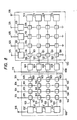
- the programmable memory type logic array (hereinbelow, termed “logic array”) is composed of a first logic array 100, a second logic array 120 and timed inverter circuits 110.
- a plurality of memory type logic cells (hereinbelow, termed “logic cells”) 101 are arranged flush in the vertical direction and lateral direction.
- the arrayed logic cells 101 have first word lines 105 arranged which are common in the vertical direction. Magnetic fluxes generated by word currents, which flow through the first word lines 105 via terminals 104 and 104', interlink with the corresponding logic cells 101.
- the arrayed logic cells 101 are connected by first bit lines 103 in the lateral direction. One end of each of the first bit lines 103 is grounded, while the other end is connected to a first bit driver circuit 102.
- the first bit driver circuits 102 are supplied with electric power through a terminal 106.
- the outputs of the first bit driver circuits 102 are respectively connected to the corresponding timed inverter circuits 111 of the timed inverter circuit group 110 through wiring leads 114.
- the timed inverter circuits 111 are supplied with electric power through a terminal 112.
- the timed inverter circuits 111 are supplied with a trigger pulse from a trigger terminal 113, and at the timing thereof, pulse signals are fed from the respective timed inverter circuits 111 to the second logic array.
- the second logic array 120 has a plurality of logic cells 101 arranged flush in the vertical direction and lateral direction.
- the logic cells 101 arrayed in the second logic array 120 have second word lines 122 arranged which are common in the lateral direction. One end of each of the second word lines 122 is connected to the corresponding timed inverter circuit 111, while the other end is connected to a corresponding terminating circuit 123. Magnetic fluxes generated by currents, which flow through the second word lines 122 from the respective timed inverter circuits 111, interlink with the logic cells 101 coupled with the second word lines 122.
- the logic cells 101 arrayed in the second logic array 120 are connected by second bit lines 124 in the vertical direction. One end of each of the second bit lines 124 is connected to a corresponding second bit driver circuit 121, while the terminal end thereof is grounded.
- the respective second bit driver circuits 121 are supplied with electric power from a terminal 126.
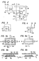
- Figure 2 shows examples of the first bit driver circuit 102 and the timed inverter circuit 111.
- the first bit driver circuit 102 is constructed of a resistor 200 one end of which is connected to the terminal 106 and the other end of which is connected to the first bit line 103 and the wiring 114.
- This timed inverter circuit 111 is described in detail in, for example, IBM Journal of research and development, Vol. 24, No. 2, March 1980 p. 143-154.
- first magnetic coupling Josephson OR circuit (Josephson Interference Device) 214, a second magnetic coupling Josephson OR circuit 215, a current injection type Josephson AND circuit 217 (Current Injection Device), a first resistor 212, a second resistor 218 and a third resistor 213.
- the wiring 114 passes near the first magnetic coupling Josephson OR circuit 214, and is terminated through a resistor 210.
- a magnetic flux generated by current which flows out through the wiring 114 from the first bit circuit 102, interlinks with the first magnetic coupling Josephson OR circuit 214.
- a wiring lead 216 is arranged near the second magnetic coupling Josephson OR circuit 215, and a magnetic flux generated by current, which is supplied to the wiring 216 from the terminal 113, interlinks with the second magnetic coupling Josephson OR circuit.
- the output of the current injection type Josephson AND circuit 217 is connected to the second word line 122.
- Figure 3 shows an example of the terminating circuit 123.
- the terminating circuit is constructed of a resistor 302 one end of which is connected to the second word line 122 and the other end of which is grounded.
- FIG. 4 shows an example of the second bit driver circuit 121.
- This second bit driver circuit 121 is constructed of a resistor 301 one end of which is connected to the terminal 126 and the other end of which is connected to an output terminal 125 as well as the second bit line 124.
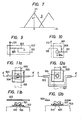
- Figures 5a and 5b and Figures 6a and 6b show the structures of the logic cells 101 for use in the first logic array 100 and second logic array 120 shown in Figure 1.
- Figure 5a is a plan view of a logic cell in a programmed state, while Figure 5b is a sectional view thereof taken along line A-A'.
- Figure 6a is a plan view of the logic cell in an unprogrammed state, while Figure 6b is a sectional view thereof taken along line A-A'.
- the logic cell shown in Figures 6a and 6b is such that a base electrode 500 and a counter electrode 501 are opposed through an insulator layer 510 which is as thin as several nm.
- a part where the base electrode 500 and the counter electrode 501 confront each other through the thin insulator layer is a Josephson junction 504.
- a control wiring lead 502 is arranged over the base electrode 500 and the counter electrode 501. These portions are stacked and formed on a substrate 550 which includes a ground plane of a superconducting material and an insulator film coverging it.
- the control wiring 502 corresponds to the first word line 105 in the first logic array 100, and to the second word line 122 in the second logic array 120.
- a base electrode 500 and a counter electrode 501 are opposed through an insulator layer 503 which is as thick as several hundred nm, and recesses are provided in parts of the thick insulator layer 503, so that the electrodes confront each other in only the recessed parts through insulator layers 510 which are as thin as several nm.
- the recessed parts serve as Josephson junctions 504.
- the two Josephson junctions 504, base electrode 500 and counter electrode 501 constitute a superconducting loop, and the so-called Josephson interferometer of the two junctions is constructed.
- Figure 7 illustrates the relationship between the maximum superconducting current Im which can flow through the logic cell shown in Figures 5a and 5b, and a control current Ic which flows through a control wiring lead 502. Since the logic cell shown in Figures 6a and 6b has a Josephson junction area larger than that of the logic cell shown in Figures 5a and 5b, the maximum superconducting current which can flow through the former logic cell is greater than in Figure 7.
- the base electrode 500 and counter electrode 501 are connected to the first bit line 103 in the first logic array 100, and to the second bit line 124 in the second logic array 120.
- bit direction In the lateral direction (hereinbelow, termed "bit direction") of the first logic array 100, the plurality of memory cells 101 are connected in series through the first bit lines 103. In a case where current is flowing through none of the first word lines 105, all the logic cells 101 are in the superconducting state, and hence, currents fed through the terminal 106 and the resistors 200 flow to the ground through the serially-connected logic cells 101.
- the serially-connected logic cells 101 have the programmed state illustrated in Figures 5a and 5b, and the unprogrammed state illustrated in Figures 6a and 6b.
- the serially-connected logic cells 101 and the first bit driver circuit 102 constitute an OR logic circuit for the signal of the wiring 114 and the signals of the first word lines 105 located in the logic cells 101 in the programmed state.
- the timed inverter circuit 111 supplies the inverted signal of the signal of the wiring 114 to the second word line 122 of the second logic array 120 at a timing which is synchronized to a trigger signal applied from the trigger terminal 113.
- An OR logic signal formed by the first logic array 100 is inverted by the timed inverter circuit, and becomes an AND signal.
- the second logic array 120 executes the OR logic operation for the signals of the second word lines 122 and delivers the resultant OR signals to the output signal terminals 125.
- a desired logic can be programmed by selectively programming the logic cells 101 which are arrayed in the logic arrays 100 and 120. That is, the desired AND signals of signals applied across the input terminals 104 and 104' are obtained in the logic array 100, and the desired OR signals of these output signals are obtained in the logic array 120, so that a desired logic signal with the OR logic and AND logic combined can be provided.
- Figure 8 shows a second embodiment according to the present invention.
- the progammable logic array shown in Figure 8 is constructed of a first logic array 100', affirmative (i.e. non-inverting) driver circuits 600 and a second logic array 120.
- the second logic array 120 in Figure 8 has the same arrangement as that of the second logic array 120 shown in Figure 1.
- the first logic array 100' in Figure 8 is constructed of logic cells 101 arrayed flush, bit driver circuits 102', first word lines 105 and first bit lines 103.
- the affirmative driver circuit group 600 is constructed of a plurality of affirmative driver circuits 601.
- Figure 9 shows an example of the bit driver circuit 102'.
- the bit driver circuit 102' has an arrangement wherein two resistors 801 and 802 are connected in series and wherein one end of the series connection is grounded, while the other end is connected to a terminal 106. The middle point of the serially-connected resistors is connected to the first word line 103.
- Figure 10 shows an example of the affirmative driver circuit 601.
- the affirmative driver circuit 601 is constructed of a current injection type Josephson AND circuit 804 and a resistor 803.
- the first bit line 103 is grounded through the current injection type Josephson AND circuit 804, the output of which is connected to the second word line 122.
- the current injection type Josephson AND circuit is described in detail in, for example, IBM Journal of research and development, Vol. 24, No. 2, March 1980.
- the current flowing through the first word line 105 and the current flowing through the first bit line 103 are subjected to the NOR logic operation, namely, AND logic operation.
- the signal of the first bit line 103 is applied to the second word line 122 by the current injection type AND circuit 804 in synchronism with a trigger signal which is applied from a trigger terminal 113.
- the operating principle that the OR logic operation is executed by the second logic array 120, is as explained with reference to Figure 1. It is apparent.from the foregoing that the programmable logic array shown in Figure 8 effects the same operations as those of the programmable logic array shown in Figure 1.
- the logic arrays used in the first and second embodiments stated above are programmed by bringing the individual logic cells 101 into the structure shown in Figures 5a and 5b or Figures 6a and 6b.
- the structures of the logic cells 101 are not restricted to those illustrated in Figures 5a and 5b and Figures 6a and 6b.
- all logic cells have the same configuration in the portions of the Josephson junctions, and the coefficients of magnetic coupling with the word lines are made unequal between the logic cells to be programmed and those not to be programmed.
- various forms can be adopted.
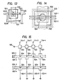
- Figures 11 a and 11 b and Figures 12a and 12b an example of the alternative structure.
- Figure 11 a is a plan view of a programmed logic cell, while Figure 11 b is a sectional view thereof taken along line A-A'.
- Figure 12a is a plan view of an unprogrammed logic cell, while Figure 12b is a sectional view thereof taken along line A-A'.
- a control wiring lead 502 passes over a Josephson junction 504, and the coefficient of magnetic coupling between them is great.
- a control wiring lead 502 is formed so as to make a detour round a Josephson junction 504, and the coefficient of magnetic coupling between them is small.
- the other symbols in these figures indicate the same members as in Figures 5a and 5b and Figures 6a and 6b, respectively.
- FIG. 13 shows still another example of the logic cell 101.
- a control line 502 is branched into a first subline 502A which passes near a Josephson junction 504 and a second subline 502B which detours round it.
- This logic cell is programmed in such a way that either a portion 510 or a portion 512 is blown out by irradiating it with a laser beam.
- a logic array employing this logic cell is demeritorious for mass-producing arrays of the same logic, but it is meritorious in case of correcting and altering logic frequently because it can be programmed immediately before its assemblage into a system.
- Figure 14 shows the setup of a still another logic cell.
- logic cells of 2 bits are comprised, and two control lines 502-1 and 502-2 are allotted to a single Josephson element.
- the control line of the logic cell namely, the word line in the logic array is formed by either a path indicated by solid lines or a path indicated by broken lines, whereby the logic cell is programmed.
- Figure 15 shows a circuit diagram in the case where the logic cell of Figure 14 is applied to the first logic array 100 of Figure 1.
- FIG. 15 shows a circuit diagram in the case where the logic cell of Figure 14 is applied to the first logic array 100 of Figure 1.
- output signals indicative of logic B-D and logic A-B-D are respectively provided from output terminals 104-1 and 114-4 by way of example.
- Figures 16 and 17 show a further example of the logic cell.
- the width of a control line 502 is made small over a Josephson interferometer as shown in Figure 16, and in the unprogrammed logic cell, it is made large as shown in Figure 17.
- the Josephson device may include a single junction or may well be a Josephson interferometer having a plurality of junctions.
- Figures 18a and 18b and Figures 19a and 19b show a yet further example of the logic cell.
- the distance between the two Josephson junctions 504 of a Josephson interferometer is made long as shown in a plan view of Figure 18a and a sectional view of Figure 18b, whereas in case of not, the distance between the two Josephson junctions 504 is made short as shown in a plan view of Figure 19a and a sectional view of Figure 19b.
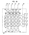
- Figure 20 shows a logic array 100" which is used instead of the first logic array 100 of the embodiment illustrated in Figure 1.
- This logic array 100" is employed in combination with the timed inverter circuits 110 and second logic array 120 explained with reference to Figure 1.
- logic cells 101' arrayed flush are connected through first bit lines 103 in the lateral direction (bit direction).
- the terminal end of the first bit line 103 is grounded, while the other end is connected to a first bit driver circuit 102.
- first bit driver circuit 102 In the vertical direction (word direction) of the logic cells 101 two common word lines 105a and 105b are arranged.
- One end of each of the two word lines 105a and 105b is connected to a terminating circuit 901, while the other end is connected to a word driver circuit 900.
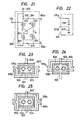
- Figure 21 shows an example of the word driver circuit 900.
- the circuit shown in Figure 21 is what is called "Self Gate AND circuit", and is described in detail in, for example, IE 3 SC-13, No. 5 (1978) 583-590 by A. Davidson.
- the circuit depicted in Figure 21 is constructed of four magnetic coupling Josephson OR circuits 910, 911, 912 and 913, and four resistors 914, 915, 916 and 917. It has the function of supplying the word line 105a with the same signal (affirmative signal) as a signal applied to a terminal 104 and supplying the word line 105b with the inverted signal thereof, in synchronism with a timing at which a voltage is applied to a terminal 902.
- Figure 22 shows an example of the terminating circuit 901. In the terminating circuit 901, the word lines 105a and 105b are grounded through resistors 916 and 917.
- Figures 23, 24 and 25 show the structures of the individual logic cells 101' in the logic array 100" of Figure 20.
- Figures 23 and 24 illustrate the structures of the logic cells in programmed states
- Figure 25 illustrates the structure of the unprogrammed logic cell.
- the affirmative signal of the signal applied to the terminal 104 is programmed in the logic cell of Figure 23, and the negative signal in the logic cell of Figure 24.
- the logic cell of Figure 23 becomes the non-superconducting state when current has flowed through the word line 105a, and the logic cell of Figure 24 becomes it when current has flowed through the word line 105b.
- both the word lines 105a and 105b detour round the logic cell. Therefore, even when currents have flowed through the word lines 105a and 105b, the logic cell remains in the superconducting state.
- the individual logic arrays 100, 100' and 120 of the foregoing embodiments fulfill the function of read-only memories which operate at high speed.
- the word lines and bit lines may be furnished with decoders for decoding address signals so as to fetch the information of desired cells in the logic array.
Landscapes
- Engineering & Computer Science (AREA)
- Computer Hardware Design (AREA)
- Physics & Mathematics (AREA)
- Computing Systems (AREA)
- General Engineering & Computer Science (AREA)
- Mathematical Physics (AREA)
- Superconductor Devices And Manufacturing Methods Thereof (AREA)
- Logic Circuits (AREA)
Claims (15)
Applications Claiming Priority (8)
| Application Number | Priority Date | Filing Date | Title |
|---|---|---|---|
| JP57125698A JPS5919294A (ja) | 1982-07-21 | 1982-07-21 | ジヨセフソン読み出し専用記憶装置 |
| JP125698/82 | 1982-07-21 | ||
| JP57125697A JPS5917725A (ja) | 1982-07-21 | 1982-07-21 | 超電導メモリ形論理アレイ |
| JP125697/82 | 1982-07-21 | ||
| JP11100382U JPS5917099U (ja) | 1982-07-23 | 1982-07-23 | メモリセル |
| JP111002/82 | 1982-07-23 | ||
| JP11100282U JPS5917098U (ja) | 1982-07-23 | 1982-07-23 | 超電導読み出し専用メモリセル |
| JP111003/82 | 1982-07-23 |
Publications (3)
| Publication Number | Publication Date |
|---|---|
| EP0112962A2 EP0112962A2 (de) | 1984-07-11 |
| EP0112962A3 EP0112962A3 (en) | 1985-01-30 |
| EP0112962B1 true EP0112962B1 (de) | 1988-12-28 |
Family
ID=27469863
Family Applications (1)
| Application Number | Title | Priority Date | Filing Date |
|---|---|---|---|
| EP83107168A Expired EP0112962B1 (de) | 1982-07-21 | 1983-07-21 | Supraleitende Festwertspeicher und programmierbare logische Felder mit solchen Speichern |
Country Status (3)
| Country | Link |
|---|---|
| US (1) | US4633439A (de) |
| EP (1) | EP0112962B1 (de) |
| DE (1) | DE3378815D1 (de) |
Families Citing this family (10)
| Publication number | Priority date | Publication date | Assignee | Title |
|---|---|---|---|---|
| JPH0691223B2 (ja) * | 1987-07-06 | 1994-11-14 | 三菱電機株式会社 | Rom装置及びその形成方法 |
| DE69032851T2 (de) * | 1989-09-29 | 1999-05-12 | Fujitsu Ltd., Kawasaki, Kanagawa | Integrierte Schaltung vom Josephson-Typ mit einer Ausgangsschnittstelle, welche die Ausgangsdaten mit reduzierter Taktfrequenz liefern kann |
| US5024993A (en) * | 1990-05-02 | 1991-06-18 | Microelectronics & Computer Technology Corporation | Superconducting-semiconducting circuits, devices and systems |
| US5424656A (en) * | 1993-05-07 | 1995-06-13 | Microelectronics And Computer Technology Corporation | Continuous superconductor to semiconductor converter circuit |
| US6148390A (en) * | 1996-06-12 | 2000-11-14 | Quicklogic Corporation | Techniques and circuits for high yield improvements in programmable devices using redundant logic |
| US9520180B1 (en) | 2014-03-11 | 2016-12-13 | Hypres, Inc. | System and method for cryogenic hybrid technology computing and memory |
| US9595970B1 (en) * | 2016-03-24 | 2017-03-14 | Northrop Grumman Systems Corporation | Superconducting cell array logic circuit system |
| US9972380B2 (en) * | 2016-07-24 | 2018-05-15 | Microsoft Technology Licensing, Llc | Memory cell having a magnetic Josephson junction device with a doped magnetic layer |
| US10756712B2 (en) | 2017-11-13 | 2020-08-25 | Northrop Grumman Systems Corporation | RQL phase-mode flip-flop |
| US10554207B1 (en) | 2018-07-31 | 2020-02-04 | Northrop Grumman Systems Corporation | Superconducting non-destructive readout circuits |
Family Cites Families (5)
| Publication number | Priority date | Publication date | Assignee | Title |
|---|---|---|---|---|
| US3626391A (en) * | 1968-07-15 | 1971-12-07 | Ibm | Josephson tunneling memory array including drive decoders therefor |
| US4039856A (en) * | 1975-12-02 | 1977-08-02 | International Business Machines Corporation | Distributed josephson junction logic circuit |
| US4151605A (en) * | 1977-11-22 | 1979-04-24 | International Business Machines Corporation | Superconducting memory array configurations which avoid spurious half-select condition in unselected cells of the array |
| US4149097A (en) * | 1977-12-30 | 1979-04-10 | International Business Machines Corporation | Waveform transition sensitive Josephson junction circuit having sense bus and logic applications |
| US4360898A (en) * | 1980-06-30 | 1982-11-23 | International Business Machines Corporation | Programmable logic array system incorporating Josephson devices |
-
1983
- 1983-07-20 US US06/515,514 patent/US4633439A/en not_active Expired - Fee Related
- 1983-07-21 DE DE8383107168T patent/DE3378815D1/de not_active Expired
- 1983-07-21 EP EP83107168A patent/EP0112962B1/de not_active Expired
Non-Patent Citations (1)
| Title |
|---|
| IBM Technical Disclosure Bulletin, Vol.17, No.7, December 1974, pp. 2059-2060; * |
Also Published As
| Publication number | Publication date |
|---|---|
| EP0112962A3 (en) | 1985-01-30 |
| EP0112962A2 (de) | 1984-07-11 |
| US4633439A (en) | 1986-12-30 |
| DE3378815D1 (en) | 1989-02-02 |
Similar Documents
| Publication | Publication Date | Title |
|---|---|---|
| EP1358655B1 (de) | Mram architektur und system | |
| EP1423855B1 (de) | Mram mit mittelpunktsreferenzgenerator | |
| US6944050B2 (en) | Nonvolatile memory device | |
| US6456524B1 (en) | Hybrid resistive cross point memory cell arrays and methods of making the same | |
| US5274593A (en) | High speed redundant rows and columns for semiconductor memories | |
| EP0443989B1 (de) | Abfühlschaltung zum Lesen von in nichtflüchtigen Speicherzellen gespeicherten Daten | |
| US4660179A (en) | Semiconductor memory device with switching for redundant cells | |
| US6778421B2 (en) | Memory device array having a pair of magnetic bits sharing a common conductor line | |
| KR101018014B1 (ko) | 차동 감지 증폭기를 포함하는 정보 저장 장치 | |
| EP0559368B1 (de) | Speicher mit Spaltenredundanz und mit örtlich begrenzten Spaltenredundanzsteuersignalen | |
| US6499111B2 (en) | Apparatus for adjusting delay of a clock signal relative to a data signal | |
| KR0179361B1 (ko) | 비휘발성 메모리 어레이 | |
| EP0112962B1 (de) | Supraleitende Festwertspeicher und programmierbare logische Felder mit solchen Speichern | |
| US4164791A (en) | Semiconductor memory with equal word line and reference line voltage drop | |
| JPS5846794B2 (ja) | メモリ・アレイ | |
| JPS6040596A (ja) | 電子装置 | |
| US5870327A (en) | Mixed mode RAM/ROM cell using antifuses | |
| US4901281A (en) | Semiconductor memory device having two column transfer gate transistor groups independently provided for a sense amplifier and a programmed circuit | |
| US4195358A (en) | Decoder for a prom | |
| CA1201529A (en) | Superconducting read-only memories or programable logic arrays having the same | |
| US20050007815A1 (en) | Magneto-resistive memory device | |
| US3441912A (en) | Feedback current switch memory cell | |
| JPH06334138A (ja) | 半導体記憶装置 | |
| JPS61267998A (ja) | プログラマブルリ−ドオンリ−メモリ | |
| JPS6151359B2 (de) |
Legal Events
| Date | Code | Title | Description |
|---|---|---|---|
| PUAI | Public reference made under article 153(3) epc to a published international application that has entered the european phase |
Free format text: ORIGINAL CODE: 0009012 |
|
| AK | Designated contracting states |
Designated state(s): DE FR GB NL |
|
| PUAL | Search report despatched |
Free format text: ORIGINAL CODE: 0009013 |
|
| AK | Designated contracting states |
Designated state(s): DE FR GB NL |
|
| 17P | Request for examination filed |
Effective date: 19841220 |
|
| 17Q | First examination report despatched |
Effective date: 19860415 |
|
| R17C | First examination report despatched (corrected) |
Effective date: 19870506 |
|
| GRAA | (expected) grant |
Free format text: ORIGINAL CODE: 0009210 |
|
| AK | Designated contracting states |
Kind code of ref document: B1 Designated state(s): DE FR GB NL |
|
| REF | Corresponds to: |
Ref document number: 3378815 Country of ref document: DE Date of ref document: 19890202 |
|
| ET | Fr: translation filed | ||
| PLBE | No opposition filed within time limit |
Free format text: ORIGINAL CODE: 0009261 |
|
| STAA | Information on the status of an ep patent application or granted ep patent |
Free format text: STATUS: NO OPPOSITION FILED WITHIN TIME LIMIT |
|
| 26N | No opposition filed | ||
| PGFP | Annual fee paid to national office [announced via postgrant information from national office to epo] |
Ref country code: DE Payment date: 19930928 Year of fee payment: 11 |
|
| PGFP | Annual fee paid to national office [announced via postgrant information from national office to epo] |
Ref country code: FR Payment date: 19940621 Year of fee payment: 12 |
|
| PGFP | Annual fee paid to national office [announced via postgrant information from national office to epo] |
Ref country code: GB Payment date: 19940711 Year of fee payment: 12 |
|
| PGFP | Annual fee paid to national office [announced via postgrant information from national office to epo] |
Ref country code: NL Payment date: 19940731 Year of fee payment: 12 |
|
| PG25 | Lapsed in a contracting state [announced via postgrant information from national office to epo] |
Ref country code: DE Effective date: 19950401 |
|
| PG25 | Lapsed in a contracting state [announced via postgrant information from national office to epo] |
Ref country code: GB Effective date: 19950721 |
|
| PG25 | Lapsed in a contracting state [announced via postgrant information from national office to epo] |
Ref country code: NL Effective date: 19960201 |
|
| GBPC | Gb: european patent ceased through non-payment of renewal fee |
Effective date: 19950721 |
|
| NLV4 | Nl: lapsed or anulled due to non-payment of the annual fee |
Effective date: 19960201 |
|
| PG25 | Lapsed in a contracting state [announced via postgrant information from national office to epo] |
Ref country code: FR Effective date: 19960430 |
|
| REG | Reference to a national code |
Ref country code: FR Ref legal event code: ST |
|
| REG | Reference to a national code |
Ref country code: FR Ref legal event code: ST |
|
| REG | Reference to a national code |
Ref country code: FR Ref legal event code: ST |