EP0113224A1 - Signalumwandlungsschaltung - Google Patents
Signalumwandlungsschaltung Download PDFInfo
- Publication number
- EP0113224A1 EP0113224A1 EP83307722A EP83307722A EP0113224A1 EP 0113224 A1 EP0113224 A1 EP 0113224A1 EP 83307722 A EP83307722 A EP 83307722A EP 83307722 A EP83307722 A EP 83307722A EP 0113224 A1 EP0113224 A1 EP 0113224A1
- Authority
- EP
- European Patent Office
- Prior art keywords
- transistor
- sub
- current
- signal
- base
- Prior art date
- Legal status (The legal status is an assumption and is not a legal conclusion. Google has not performed a legal analysis and makes no representation as to the accuracy of the status listed.)
- Granted
Links
Images

Classifications
-
- G—PHYSICS
- G11—INFORMATION STORAGE
- G11B—INFORMATION STORAGE BASED ON RELATIVE MOVEMENT BETWEEN RECORD CARRIER AND TRANSDUCER
- G11B5/00—Recording by magnetisation or demagnetisation of a record carrier; Reproducing by magnetic means; Record carriers therefor
- G11B5/02—Recording, reproducing, or erasing methods; Read, write or erase circuits therefor
- G11B5/027—Analogue recording
- G11B5/03—Biasing
-
- G—PHYSICS
- G11—INFORMATION STORAGE
- G11B—INFORMATION STORAGE BASED ON RELATIVE MOVEMENT BETWEEN RECORD CARRIER AND TRANSDUCER
- G11B5/00—Recording by magnetisation or demagnetisation of a record carrier; Reproducing by magnetic means; Record carriers therefor
- G11B5/02—Recording, reproducing, or erasing methods; Read, write or erase circuits therefor
- G11B5/027—Analogue recording
Definitions
- This invention relates to signal translating circuits.
- Such circuits are, for example, suitable for use in a recording amplifier provided for recording a video signal in a video tape recorder of the helical scanning type.
- FIG. 1 There has been previously proposed a circuit as shown in Figure 1 of the accompanying drawings for forming a recording amplifier used for recording a video signal in a video tape recorder of the helical scanning type.
- the circuit of Figure 1 contains therein a signal translating circuit performing voltage to current conversion, a major part of which is formed into an integrated circuit 10 comprising transistors Q1 to Q9 which are arranged on a common semiconductor substrate.
- the transistors Q 1 and Q 2 form an input current mirror circuit portion which is supplied with a DC biasing current I B flowing therethrough by the transistor Q 3 having its base supplied with a DC voltage V 1 .
- the transistors Q 5 to Q 8 form an output current mirror circuit portion, and the transistor Q 9 forms an output stage.
- each of the transistors Q 8 and Q 9 is designed to be approximately fifty times as large in area as that of each of the transistors Q 1 to Q 7 .
- An input terminal 11 is provided at the emitter of the transistor Q 2 which is connected to act as a diode, and an output terminal 12 is provided at the collector of the transistor Q 9 .
- a power supply terminal 13 and a ground terminal 14 are also provided.
- a source 20 of a video signal which is to be recorded is connected through a resistor R 1 and a capacitor C 1 to the input terminal 11, and a primary winding of a rotary transformer 30 is connected between the output terminal 12 and the power supply terminal 13.
- a secondary winding of the rotary transformer 30 is coupled with a coil of a magnetic head 40.
- the resistance value in the forward direction of the transistor 0 2 connected to act as a diode and forming the input current mirror circuit portion varies in response to a current flowing therethrough, and consequently an input signal current i IN suffers from second harmonic distortion.
- a signal translating circuit comprising:
- the input current signal can be made almost free from the problem of distortion over the whole range in which the second transistor is in the active state, and therefore a DC biasing current flowing through the second transistor can be reduced to a value corresponding to a half of the peak-to-peak value of the input current signal.
- the power consumption in the circuit can be considerably reduced.
- both DC and AC components of the output current signal are determined substantially externally of the integrated circuit, and an output current signal which is not substantially affected by temperature variations of the integrated circuit can be obtained.
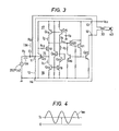
- Figure 3 shows an embodiment of signal translating circuit according to the invention which performs voltage to current conversion and is used as a recording amplifier for recording a video signal in a video tape recorder of the helical scanning type.
- a major part of the circuit is formed into the integrated circuit 10 which comprises transistors Q11 to Q 22 arranged on a common semiconductor substrate.
- the transistors Q 11 and Q12 are connected to each other in such a manner that the collector of the transistor Q 11 is coupled through a resistor R12 provided for preventing oscillation to the base of the transistor Q 12 , and the emitter of the transistor Q 12 is coupled with the base of the transistor Q 11 , so as to form a negative feedback circuit 15.
- the transistor Q 13 connected to the emitter of the transistor Q 12 forms a first constant current source 17.
- the transistors Q 13 and Q 16 to Q 18 inclusive form a current mirror circuit connected to a third constant current source formed by the transistor Q 15'
- the transistors Q 19 to Q 22 inclusive form a current mirror amplifying circuit, and the transistor Q 22 individually forms an output stage.
- the emitter of the transistor Q 22 is designed to be approximately fifty times as large in area as that of each of the transistors Q 11 to Q 21 .
- the input terminal 11 is connected to the base of the transistor Q 11 , which is a feedback point in the negative feedback circuit 15, and the output terminal 12 is connected to the collector of the transistor Q 22 .
- a biasing resistor R B is connected between the input terminal 11 and the power supply terminal 13.
- the source 20 of the video signal (input voltage signal e IN ) which is to be recorded is connected through the resistor R 1 and the capacitor C l to the input terminal 11, and the rotary transformer 30 to which the magnetic head 40 is coupled is connected between the output terminal 12 and the power supply terminal 13.
- the input voltage signal e IN from the source 20 is supplied to the resistor R 1 to be converted thereby into the input current signal i IN , and the input current signal i IN thus obtained is supplied to the input terminal 11.
- the transistor Q 14' which forms the second constant current source is maintained in the active state in consequence of being supplied with a voltage V 3 to the base thereof, and supplies a constant current i 2 therefrom.
- the transistor Q 15' which forms the third constant current source is also maintained in the active state in consequence of being supplied with the voltage V 3 to the base thereof and supplies a constant current I3 flowing therethrough into the current mirror circuit formed by the transistors Q 13 and Q 16 to Q 18 .
- a constant current I I flows through the transistor Q 13 in response to the constant current I 3 flowing through the transistors Q 17 and Q 18 due to the current mirror operation therein.
- the constant current I 2 of the second constant current source 17 and the constant current I 3 of the third current source are determined to be equal to each other and the constant current I 1 of the first constant current source 16 and the constant current I 3 are also determined to be equal to each other, so that the constant current I 1 is equal to the constant current I 2 .
- an output current signal which is obtained in response to the input current signal i IN supplied to the negative feedback circuit 15, is supplied to the current mirror amplifying circuit formed by the transistors Q19 to Q 22 inclusive from the collector of the transistor Q 12' and an amplified output current signal is supplied to the rotary transformer 30 through the transistor Q 22 which forms the output stage.
- a recording current flows through the magnetic head 40 in response to the amplified output current signal supplied to the rotary transformer 30.
- the input terminal 11 since the input terminal 11, to which the input current signal i IN is supplied, is provided at the base of the transistor Q 11 forming the feedback point in the negative feedback circuit 15 formed by the transistors Q 11 and Q 12 ' and consequently the potential of the input terminal 11 is maintained constant, the input impedance at the input terminal 11 viewed from the source 20 becomes substantially zero. Accordingly, the input current signal i IN depends upon only the input voltage signal e IN from the source 20 and the resistor R 1 , and the following equation is satisfied: wherein i IN , e IN and R 1 stand for the current value of the input current value of the input current signal i IN , the voltage value of the input voltage signal e IN and the resistance value of the resistor R 1 .
- the difference between the constant current I 2 of the second constant current source 17 and a DC current I4 contained in the output current signal is equal to the difference between the constant current I1 of the first constant current source 16 and a DC biasing current I IN supplied through the biasing resistor R B provided externally of the integrated circuit 10, that is, the equation: is satisfied.
- the DC current I4 contained in the output current signal is equal to the DC biasing current I IN flowing through the biasing resistor R B , and assuming that a power source voltage V CC is supplied to the power supply terminal 13, and a base-emitter voltage V BE is obtained between the base and emitter of the transistor Q 11 , the following equation is satisfied: where R B stands for the resistance value of the biasing resistor R B . Accordingly, the DC current contained in the output current signal is substantially determined by the arrangement external to the integrated circuit 10. In one specific example, I 1 and I 2 are selected to be 300 microamps, I IN and 1 4 are selected to be 500 microamps and a DC current flowing through the transistor Q 22 is selected to be 40 milliamps.
- the DC biasing current can be reduced to a value corresponding to the peak value of the input current signal and, as a result, the power consumption can be considerably reduced.
- the output current signal which is determined in accordance with the arrangement provided externally of the integrated circuit and is not substantially affected by temperature variations in the integrated circuit is derived, and therefore a stable recording current based on such a output current signal can be obtained in the case where the circuit is used as a recording amplifier in a video tape recorder.
Landscapes
- Amplifiers (AREA)
Applications Claiming Priority (2)
| Application Number | Priority Date | Filing Date | Title |
|---|---|---|---|
| JP234248/82 | 1982-12-30 | ||
| JP57234248A JPS59125106A (ja) | 1982-12-30 | 1982-12-30 | 電圧−電流変換回路 |
Publications (2)
| Publication Number | Publication Date |
|---|---|
| EP0113224A1 true EP0113224A1 (de) | 1984-07-11 |
| EP0113224B1 EP0113224B1 (de) | 1987-03-25 |
Family
ID=16967989
Family Applications (1)
| Application Number | Title | Priority Date | Filing Date |
|---|---|---|---|
| EP83307722A Expired EP0113224B1 (de) | 1982-12-30 | 1983-12-19 | Signalumwandlungsschaltung |
Country Status (5)
| Country | Link |
|---|---|
| US (1) | US4559501A (de) |
| EP (1) | EP0113224B1 (de) |
| JP (1) | JPS59125106A (de) |
| CA (1) | CA1214269A (de) |
| DE (1) | DE3370554D1 (de) |
Families Citing this family (2)
| Publication number | Priority date | Publication date | Assignee | Title |
|---|---|---|---|---|
| JP3086768B2 (ja) * | 1993-06-30 | 2000-09-11 | 株式会社東芝 | 磁気記録再生装置用増幅回路 |
| US5398004A (en) * | 1994-02-09 | 1995-03-14 | Trw Inc. | HBT direct-coupled low noise wideband microwave amplifier |
Citations (2)
| Publication number | Priority date | Publication date | Assignee | Title |
|---|---|---|---|---|
| US3651347A (en) * | 1970-09-28 | 1972-03-21 | Rca Corp | Signal translating stage providing direct voltage translation independent of supplied operating potential |
| US4354122A (en) * | 1980-08-08 | 1982-10-12 | Bell Telephone Laboratories, Incorporated | Voltage to current converter |
Family Cites Families (2)
| Publication number | Priority date | Publication date | Assignee | Title |
|---|---|---|---|---|
| GB840666A (en) * | 1957-03-01 | 1960-07-06 | British Telecomm Res Ltd | Improvements in or relating to amplifiers employing transistors |
| US4268798A (en) * | 1977-12-19 | 1981-05-19 | Motorola, Inc. | High performance summing amplifier |
-
1982
- 1982-12-30 JP JP57234248A patent/JPS59125106A/ja active Pending
-
1983
- 1983-12-19 DE DE8383307722T patent/DE3370554D1/de not_active Expired
- 1983-12-19 EP EP83307722A patent/EP0113224B1/de not_active Expired
- 1983-12-20 CA CA000443842A patent/CA1214269A/en not_active Expired
- 1983-12-22 US US06/564,099 patent/US4559501A/en not_active Expired - Lifetime
Patent Citations (2)
| Publication number | Priority date | Publication date | Assignee | Title |
|---|---|---|---|---|
| US3651347A (en) * | 1970-09-28 | 1972-03-21 | Rca Corp | Signal translating stage providing direct voltage translation independent of supplied operating potential |
| US4354122A (en) * | 1980-08-08 | 1982-10-12 | Bell Telephone Laboratories, Incorporated | Voltage to current converter |
Also Published As
| Publication number | Publication date |
|---|---|
| US4559501A (en) | 1985-12-17 |
| CA1214269A (en) | 1986-11-18 |
| DE3370554D1 (en) | 1987-04-30 |
| EP0113224B1 (de) | 1987-03-25 |
| JPS59125106A (ja) | 1984-07-19 |
Similar Documents
| Publication | Publication Date | Title |
|---|---|---|
| EP0072589A2 (de) | Stromstabilisierungsanordnung | |
| JPH07271461A (ja) | 安定化電圧発生制御回路 | |
| US4740766A (en) | Precision tracking current generator | |
| US3828241A (en) | Regulated voltage supply circuit which compensates for temperature and input voltage variations | |
| US7075358B1 (en) | Base current compensation for a bipolar transistor current mirror circuit | |
| EP0113224A1 (de) | Signalumwandlungsschaltung | |
| US5378938A (en) | Sample-and-hold circuit including push-pull transconductance amplifier and current mirrors for parallel feed-forward slew enhancement and error correction | |
| US5285170A (en) | Operational amplifier with all NPN transistor output stage | |
| US4453134A (en) | High voltage operational amplifier | |
| US4580177A (en) | Switching circuit for AC bias signal | |
| US4417292A (en) | Power amplifier protection circuit | |
| US4356455A (en) | Amplifier | |
| US4573019A (en) | Current mirror circuit | |
| US3675142A (en) | Transistor power amplifier with dc output voltage stabilization | |
| JP3057337B2 (ja) | 基準電圧発生回路 | |
| US5506536A (en) | Differential amplifier with exponential gain characteristic | |
| JPS6343923B2 (de) | ||
| JP3041917B2 (ja) | ピークホールド回路 | |
| US6424324B1 (en) | Display driver apparatus | |
| US4485350A (en) | Variable electronic impedance circuit | |
| US5014019A (en) | Amplifier circuit operable at low power source voltage | |
| JPH0588767A (ja) | バンドギヤツプリフアレンス回路 | |
| JP3534275B2 (ja) | 電流源及び集積回路 | |
| JP3221058B2 (ja) | 整流回路 | |
| JPH0716138B2 (ja) | 増幅回路装置 |
Legal Events
| Date | Code | Title | Description |
|---|---|---|---|
| PUAI | Public reference made under article 153(3) epc to a published international application that has entered the european phase |
Free format text: ORIGINAL CODE: 0009012 |
|
| AK | Designated contracting states |
Designated state(s): DE FR GB NL |
|
| 17P | Request for examination filed |
Effective date: 19841122 |
|
| GRAA | (expected) grant |
Free format text: ORIGINAL CODE: 0009210 |
|
| AK | Designated contracting states |
Kind code of ref document: B1 Designated state(s): DE FR GB NL |
|
| REF | Corresponds to: |
Ref document number: 3370554 Country of ref document: DE Date of ref document: 19870430 |
|
| ET | Fr: translation filed | ||
| PLBE | No opposition filed within time limit |
Free format text: ORIGINAL CODE: 0009261 |
|
| STAA | Information on the status of an ep patent application or granted ep patent |
Free format text: STATUS: NO OPPOSITION FILED WITHIN TIME LIMIT |
|
| 26N | No opposition filed | ||
| PGFP | Annual fee paid to national office [announced via postgrant information from national office to epo] |
Ref country code: FR Payment date: 20011212 Year of fee payment: 19 |
|
| PGFP | Annual fee paid to national office [announced via postgrant information from national office to epo] |
Ref country code: GB Payment date: 20011219 Year of fee payment: 19 |
|
| PGFP | Annual fee paid to national office [announced via postgrant information from national office to epo] |
Ref country code: NL Payment date: 20011228 Year of fee payment: 19 |
|
| REG | Reference to a national code |
Ref country code: GB Ref legal event code: IF02 |
|
| PGFP | Annual fee paid to national office [announced via postgrant information from national office to epo] |
Ref country code: DE Payment date: 20020109 Year of fee payment: 19 |
|
| PG25 | Lapsed in a contracting state [announced via postgrant information from national office to epo] |
Ref country code: GB Free format text: LAPSE BECAUSE OF NON-PAYMENT OF DUE FEES Effective date: 20021219 |
|
| PG25 | Lapsed in a contracting state [announced via postgrant information from national office to epo] |
Ref country code: NL Free format text: LAPSE BECAUSE OF NON-PAYMENT OF DUE FEES Effective date: 20030701 Ref country code: DE Free format text: LAPSE BECAUSE OF NON-PAYMENT OF DUE FEES Effective date: 20030701 |
|
| GBPC | Gb: european patent ceased through non-payment of renewal fee |
Effective date: 20021219 |
|
| NLV4 | Nl: lapsed or anulled due to non-payment of the annual fee |
Effective date: 20030701 |
|
| PG25 | Lapsed in a contracting state [announced via postgrant information from national office to epo] |
Ref country code: FR Free format text: LAPSE BECAUSE OF NON-PAYMENT OF DUE FEES Effective date: 20030901 |
|
| REG | Reference to a national code |
Ref country code: FR Ref legal event code: ST |