EP0113517A2 - Verfahren zur Herstellung einer Isolationszone - Google Patents
Verfahren zur Herstellung einer Isolationszone Download PDFInfo
- Publication number
- EP0113517A2 EP0113517A2 EP83307091A EP83307091A EP0113517A2 EP 0113517 A2 EP0113517 A2 EP 0113517A2 EP 83307091 A EP83307091 A EP 83307091A EP 83307091 A EP83307091 A EP 83307091A EP 0113517 A2 EP0113517 A2 EP 0113517A2
- Authority
- EP
- European Patent Office
- Prior art keywords
- groove
- layer
- oxygen
- insulating layer
- metal
- Prior art date
- Legal status (The legal status is an assumption and is not a legal conclusion. Google has not performed a legal analysis and makes no representation as to the accuracy of the status listed.)
- Granted
Links
Images




Classifications
-
- H—ELECTRICITY
- H10—SEMICONDUCTOR DEVICES; ELECTRIC SOLID-STATE DEVICES NOT OTHERWISE PROVIDED FOR
- H10P—GENERIC PROCESSES OR APPARATUS FOR THE MANUFACTURE OR TREATMENT OF DEVICES COVERED BY CLASS H10
- H10P14/00—Formation of materials, e.g. in the shape of layers or pillars
- H10P14/60—Formation of materials, e.g. in the shape of layers or pillars of insulating materials
- H10P14/61—Formation of materials, e.g. in the shape of layers or pillars of insulating materials using masks
-
- H—ELECTRICITY
- H10—SEMICONDUCTOR DEVICES; ELECTRIC SOLID-STATE DEVICES NOT OTHERWISE PROVIDED FOR
- H10P—GENERIC PROCESSES OR APPARATUS FOR THE MANUFACTURE OR TREATMENT OF DEVICES COVERED BY CLASS H10
- H10P50/00—Etching of wafers, substrates or parts of devices
- H10P50/69—Etching of wafers, substrates or parts of devices using masks for semiconductor materials
- H10P50/691—Etching of wafers, substrates or parts of devices using masks for semiconductor materials for Group V materials or Group III-V materials
-
- H—ELECTRICITY
- H10—SEMICONDUCTOR DEVICES; ELECTRIC SOLID-STATE DEVICES NOT OTHERWISE PROVIDED FOR
- H10P—GENERIC PROCESSES OR APPARATUS FOR THE MANUFACTURE OR TREATMENT OF DEVICES COVERED BY CLASS H10
- H10P76/00—Manufacture or treatment of masks on semiconductor bodies, e.g. by lithography or photolithography
- H10P76/40—Manufacture or treatment of masks on semiconductor bodies, e.g. by lithography or photolithography of masks comprising inorganic materials
-
- H—ELECTRICITY
- H10—SEMICONDUCTOR DEVICES; ELECTRIC SOLID-STATE DEVICES NOT OTHERWISE PROVIDED FOR
- H10W—GENERIC PACKAGES, INTERCONNECTIONS, CONNECTORS OR OTHER CONSTRUCTIONAL DETAILS OF DEVICES COVERED BY CLASS H10
- H10W10/00—Isolation regions in semiconductor bodies between components of integrated devices
- H10W10/01—Manufacture or treatment
- H10W10/011—Manufacture or treatment of isolation regions comprising dielectric materials
- H10W10/012—Manufacture or treatment of isolation regions comprising dielectric materials using local oxidation of silicon [LOCOS]
-
- H—ELECTRICITY
- H10—SEMICONDUCTOR DEVICES; ELECTRIC SOLID-STATE DEVICES NOT OTHERWISE PROVIDED FOR
- H10W—GENERIC PACKAGES, INTERCONNECTIONS, CONNECTORS OR OTHER CONSTRUCTIONAL DETAILS OF DEVICES COVERED BY CLASS H10
- H10W10/00—Isolation regions in semiconductor bodies between components of integrated devices
- H10W10/01—Manufacture or treatment
- H10W10/011—Manufacture or treatment of isolation regions comprising dielectric materials
- H10W10/014—Manufacture or treatment of isolation regions comprising dielectric materials using trench refilling with dielectric materials, e.g. shallow trench isolations
-
- H—ELECTRICITY
- H10—SEMICONDUCTOR DEVICES; ELECTRIC SOLID-STATE DEVICES NOT OTHERWISE PROVIDED FOR
- H10W—GENERIC PACKAGES, INTERCONNECTIONS, CONNECTORS OR OTHER CONSTRUCTIONAL DETAILS OF DEVICES COVERED BY CLASS H10
- H10W10/00—Isolation regions in semiconductor bodies between components of integrated devices
- H10W10/01—Manufacture or treatment
- H10W10/041—Manufacture or treatment of isolation regions comprising polycrystalline semiconductor materials
-
- H—ELECTRICITY
- H10—SEMICONDUCTOR DEVICES; ELECTRIC SOLID-STATE DEVICES NOT OTHERWISE PROVIDED FOR
- H10W—GENERIC PACKAGES, INTERCONNECTIONS, CONNECTORS OR OTHER CONSTRUCTIONAL DETAILS OF DEVICES COVERED BY CLASS H10
- H10W10/00—Isolation regions in semiconductor bodies between components of integrated devices
- H10W10/10—Isolation regions comprising dielectric materials
- H10W10/13—Isolation regions comprising dielectric materials formed using local oxidation of silicon [LOCOS], e.g. sealed interface localised oxidation [SILO] or side-wall mask isolation [SWAMI]
-
- H—ELECTRICITY
- H10—SEMICONDUCTOR DEVICES; ELECTRIC SOLID-STATE DEVICES NOT OTHERWISE PROVIDED FOR
- H10W—GENERIC PACKAGES, INTERCONNECTIONS, CONNECTORS OR OTHER CONSTRUCTIONAL DETAILS OF DEVICES COVERED BY CLASS H10
- H10W10/00—Isolation regions in semiconductor bodies between components of integrated devices
- H10W10/10—Isolation regions comprising dielectric materials
- H10W10/17—Isolation regions comprising dielectric materials formed using trench refilling with dielectric materials, e.g. shallow trench isolations
-
- H—ELECTRICITY
- H10—SEMICONDUCTOR DEVICES; ELECTRIC SOLID-STATE DEVICES NOT OTHERWISE PROVIDED FOR
- H10W—GENERIC PACKAGES, INTERCONNECTIONS, CONNECTORS OR OTHER CONSTRUCTIONAL DETAILS OF DEVICES COVERED BY CLASS H10
- H10W10/00—Isolation regions in semiconductor bodies between components of integrated devices
- H10W10/40—Isolation regions comprising polycrystalline semiconductor materials
Definitions
- the present invention relates to a method for forming an isolation region for electrically isolating of a semiconductor device, elements /more particularly, to a method for forming an isolation region by which a semiconductor device having a high integration density can be produced.
- an isolation region i.e., a region for isolating elements from each other, formed by the steps of forming a silicon nitride (Si 3 N 4 ) layer on a silicon substrate, patterning the silicon nitride, and then forming a silicon dioxide layer by thermal oxidation of the surface of the silicon substrate using the patterned silicon nitride layer as a masking film.
- the silicon layer located below the edge portion of the silicon nitride layer is simultaneously oxidized.
- the resultant silicon dioxide layer raises the edge portion of the silicon nitride layer.
- This silicon dioxide layer commonly called a "bird's beak" due to its configuration, extends to the active region and therefore decreases the possible integration density.
- grooves are formed in the surface portion of the silicon substrate by a photolithography technique. Thermal oxidation or a chemical vapor deposition (CVD) process is then used to form an insulating layer on the grooves, thereby effecting element isolation.
- CVD chemical vapor deposition
- the smallest possible width of the grooves formed in the surface of the silicon substrate, namely, the width of at least the isolation region, is presently / 1 ⁇ m due to limitations of the photolithography process. It has not been possible until now to form submicron-width isolation regions.
- An embodiment of the present invention can provide a method for forming an isolation region having an submicron width.
- An embodiment of the present invention can also provide a method for forming an isolation region which does not require a fine photolithography process.
- An embodiment of the present invention can also provide a method for forming isolation regions for semiconductor devices such as bipolar transistors or metal oxide semiconductor allowing (MOS) transistors. / a high integration density.
- semiconductor devices such as bipolar transistors or metal oxide semiconductor allowing (MOS) transistors. / a high integration density.
- a method for forming an isolation region for electrically isolating elements in a semiconductor substrate comprising the steps of: forming a metal or metal silicide layer on the semiconductor substrate; forming a resist layer on the metal or metal silicide layer; patterning the resist layer; selectively etching the metal or metal silicide layer and the semiconductor substrate by a reactive ion etching process using a mixture of chlorine-containing gas and oxygen gas to form a groover in the surface portion of the semiconductor substrate around the edge of the resist layer; and forming an insulating layer in the groove.
- a method for forming an isolation region for electrically isolating elements in a semiconductor substrate comprising the steps of: forming in turn, a first insulating layer, a metal or metal silicide layer, and resist layer; patterning.the resist layer; selectively etching the metal or metal silicide layer by the reactive ion etching process using a mixture of chlorine-containing gas and oxygen gas; etching the first insulating layer using the metal or metal silicide layer as a masking film; etching the semiconductor substrate using the patterned first insulating layer as a masking film to form a groove in the surface portion of the semiconductor substrate; and forming a second insulating layer in the groove.
- a method for forming an isolation region for electrically isolating elements in a semiconductor substrate comprises the steps of: forming a metal or a metal silicide layer on the semiconductor substrate; forming a resist layer on the metal or metal silicide layer; patterning the resist layer; selectively etching the metal or metal silicide layer and the semiconductor substrate by a reactive ion etching process using a mixture of chlorine-containing gas and oxygen gas to form a groove in the surface portion of the semiconductor- substrate around the edge of the resist layer; and forming an insulating layer in the groove.
- the metal be selected from the group consisting of molybdenum, tungsten, titanium, platinum, and tantalum; that the metal silicide be selected from the group consisting of molybdenum silicide, tungsten silicide, titanium silicide, platinum silicide, and tantalum silicide, and that the chlorine-containing gas be selected from the group consisting of carbon tetrachloride, silicon tetrachloride and boron tetrachloride.
- the reactive ion etching can be advantageously carried out using a mixed gas (gas mixture) of oxygen and carbon tetrachloride at a power density of 0.14 to 0.35 W/cm 2 and degree of vacuum (pressure) of 1 to 10 Pa, for 1 to 9 or 3 to 30 minutes,-the volume percentage of oxygen in the mixed gas of oxygen and the carbon tetrachloride being 60% to 70%.
- a mixed gas gas mixture
- degree of vacuum pressure
- the insulating layer in the groove is preferably formed by a thermal oxidation process at a temperature of 800°C to 1100 0 C under a wet oxidation atmosphere or by a CVD process or, further, by the steps comprising oxidizing the whole inner wall of the groove by the thermal oxidation process; burying the-groove in polycrystalline silicon by a CVD process.
- the exposed surface of polycrystalline silicon in said groove may be oxidised by thermal oxidation.
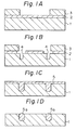
- Figures 1A to ID are schematic cross-sectional views for explaining an example of steps according to the present invention.
- / molybdenum silicide (MoSi 2 ) - layer 2 about 0.3 ⁇ m thick is formed on a silicon substrate 1 by the D.C. magnetron sputtering process.
- the resist layer 3 is then patterned to obtain a required form.
- the molybdenum silicide layer 2 and the silicon substrate 1 are etched by the reactive ion etching process.
- the reactive ion etching process is carried out by using a gas mixture of 70% oxygen and 30% carbon tetrachloride; at a power density of 0.28 W/cm 2 , a pressure of 4 Pa, and an etching time of 9 minutes.
- the molybdenum silicide layer 2 located around the edge of the resist layer 3 is first etched; then the surface of the silicon substrate 1 located around the edge of the resist layer 3 is etched so as to make grooves 4 having a width of 0.3 pm and a depth of 0.8 ⁇ m.
- peripheral etching is carried out so that the edge of the resist must be positioned at a required pattern.
- the resist layer 3 and the molybdenum silicide layer 2 are then removed by the oxygen plasma ashing and wet etching processes respectively.
- Silicon dioxide (Si0 2 ) layer 5 having a thickness of approximately 0.3 ⁇ m over the silicon substrate 1, which thickness is the same level as the width of the prior grooves 4.
- the width of the silicon dioxide layer formed in the grooves is approximately 0.6 ⁇ m, twice the width of the grooves.
- the silicon dioxide layer 5 over the top surface of silicon substrate 1 is removed by the normal wet etching process, leaving the silicon dioxide in the grooves 4 as buried silicon dioxide regions 5a.
- the surface of the buried silicon dioxide regions 5a is substantially flat.
- the silicon dioxide regions 5a act as isolation regions for a variety of semiconductor devices. Alternative processes for forming isolation regions in the grooves will be described later.
- Another.method for forming an isolation region for electrically isolating elements in a semiconductor substrate comprises the steps of: forming in turn, a first insulating layer, a metal or a metal silicide layer, and resist layer; patterning the resist layer; selectively etching the metal or metal silicide layer by the reactive ion etching process.using a mixture of chlorine-containing gas and oxygen gas; etching the insulating layer using the metal.or metal silicide layer as a masking film; etching the semiconductor substrate using the patterned insulating layer as a masking film to form a groove in the surface portion of the semiconductor substrate; and forming a second insulating layer in the groove.
- the first insulating layer is preferably composed of either silicon nitride or silicon dioxide.
- the etching of the metal or metal silicide layer is advantageously carried out by a reactive ion etching process using a mixture of oxygen and carbon tetrachloride at a power density of 0.14 to 0.35 W/cm2 and a pressure of 1 to 10 Pa, for 1 to 9 minutes, the volume percentage of oxygen in the mixture being 60% to 70%.
- the etching of the first insulating layer to form the groove is advantageously carried out by a reactive ion etching process using an etching gas of trifluoromethane at a power density of 0.06 to 0.8 W/cm 2 and pressure of 0.9 to 13 Pa, for 3 to 30 minutes.
- the etching of the semiconductor substrate can be carried out by a reactive ion etching process using a mixture of oxygen and carbon tetrachloride at a power density of 0.14 to 0.35 W/cm 2 and a pressure of 1 to 10 Pa, for 3 to 30 minutes, the volume percentage of oxygen in the mixture being less than 50.
- the second insulating layer can be formed in the same ways as described for the insulating layer of the first method.
- Figures 2A to 2F are schematic cross-sectional views for explaining an example of steps according to according to this other method / the present invention.
- an insulating layer 4 about 0.1 ⁇ m thick and consisting of, for example, silicon nitride (Si 3 N 4 ) is formed on a silicon substrate 1 by the CVD process.
- a metal silicide layer 2 about 0.3 ⁇ m thick and consisting of, for example, molybdenum silicide is formed on the insulating layer 4 by the D.C. magnetron sputtering process.
- the metal silicide layer 2 located around the edge of the resist layer 3 is then etched by the reactive ion etching process to form grooves 5.
- the reactive ion etching process is carried under out :/ the same etching conditions as in Fig. 1B.
- the resulting grooves 5 have a width D of 0.2 to 0.3 ⁇ m.
- the etching gas in the parallel-plate-type reactive ion etching apparatus is then changed to trifluoromethane (CHF 3 ), and the exposed insulating layer 4 is etched by the reactive ion etching process under a power density of 0.16 W/cm 2 , a pressure of 6.7 Pa, and an etching time of 15 minutes, using patterned metal silicide layer 2 and resist layer 3 as a mask.
- CHF 3 trifluoromethane
- the resist layer 3 is then removed by the ashing process.
- the etching gas in the parallel-plate-type reactive ion etching apparatus is changed to a gas which will etch the metal silicide layer 2 and the silicon substrate 1 but not easily etch the insulating layer 4, for example a mixture by volume of 20% oxygen and 80% carbon tetrachloride, and etching ds con- ducted at a power density of 0.28 W/cm 2 , pressure of 4 Pa, and an etching time of 5 minutes.
- thermal oxidation is then effected at a temperature of 1000°C under a wet oxidizing atmosphere to form an insulating layer 7 consisting of silicon dioxide, which acts as an isolation region.
- the width of the silicon dioxide layer formed in the groove is approximately 0.4 to 0.6 ⁇ m, twice the width of the grooves 6.
- the insulating layer 4 at the surface is removed by a wet etching process using phosphoric acid at 180°C to leave isolation regions in the grooves of submicron width.
- the volume percentage of the oxygen in the mixture is preferably from 60% to 70% as stated before.
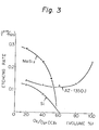
- Figure 3 shows the relationship between the oxygen volume percentage in the gas mixture and the etching rate obtained by using a parallel-plate-type reactive ion etching.device under the etching conditions mentioned above.
- the metal silicide and resist used were the same as in Fig. lA, i.e., molybdenum silicide and AZ-1350J produced by SHIPLEY CO.
- Fig. 3 when the volume percentage of oxygen in the gas mixture is less than 50%, the molybdenum silicide layer and the silicon substrate not covered by resist can be etched.
- the volume percentage of oxygen is 80% or more, only ashing of the resist occurs and the molybdenum silicide layer and silicon substrate are not etched.
- the reason for this is thought to be that an oxide layer forms over the surface of the molybdenum silicide layer.
- reactive ion etching is carried out using a volume percentage of oxygen in the gas mixture of from 60% to 70%, only the molybdenum silicide layer and the silicon substrate located around the edge of the resist layer are etched.
- the explanation is thought to be that a large amount of oxygen is used for oxidation of the surface of the molybdenum silicide. and the ashing of the resist layer, so the volume percentage of oxygen in the gas around the edge of the.resist layer becomes less than 50%, the molybdenum silicide layer under such oxygen is etched, and then the silicon substrate is etched.
- Figure 4 illustrates the relationship between the etching time and etching width at an oxygen volume of 70% in the mixture of oxygen and carbon tetrachloride, a power density of 0.28 W/cm 2 , and a pressure of 4 Pa. This graph shows that a submicron width groove can be obtained in the silicon substrate within five minutes.
- Alternative processes for forming the insulating layer of the first method and the second insulating layer of the second method, so as to provide isolation regions, are now described.
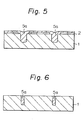
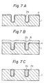
- Figures 5, 6, and 7A to 7C are schematic cross-sectional views for explaining alternative processes for forming isolation regions in the grooves of the substrate.
- a thermal oxidation processes performed under the same conditions.as in the step of Fig. 1C.
- the silicon dioxide layer and the molybdenum silicide layer 2 over the silicon substrate 1 are removed, leaving the silicon dioxide in the groove 4 as the buried silicon dioxide regions 5a.
- the molybdenum silicide layer 2 is slightly oxidized, thereby decreasing in thickness.
- silicon dioxide is deposited in the grooves and on the surface of the silicon substrate 1 by the CVD process. Then, the silicon dioxide layer on the surface of the silicon substrate 1 is removed to form the isolation regions 5a having a width of the grooves 4, i.e., 0.3 pm.
- a third alternative /r.eferring to Figs. 7A to 7C, after removing the resist layer 3 and the molybdenum silicide layer 2 as in Fig. 1B or the step of Fig. 2D, as shown in Fig. 7A, the inner wall of the grooves in the silicon substrate 1 is slightly oxidized by a thermal oxidation process to form a silicon dioxide layer 2b.
- a polycrystalline silicon layer 8 is then deposited over the silicon substrate by the well known Low Pressure CVD process to bury the grooves.
- the deposited polycrystalline silicon layer 8 is removed by polishing to provide a flat surface by using the silicon nitride 4 as a mask.
- anisotropic dry etching may be used to provide the flat surface.
- the exposed polycrystalline silicon above the grooves is oxidized by the thermal oxidation process to make a silicon dioxide layer 2C having a slight thickness of 0.3 ⁇ m.
- the silicon insulating layer 4 such as silicon nitride is removed.
- isolation regions are produced.
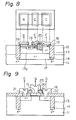
- I solation regions obtained by/the present invention can be applied to, for example, a bipolar transistor or MOS transistor.
- Figures 8 and 9 are schematic views for explaining applications of the present invention to a bipolar transistor and NMOS trasistor, respectively.
- reference numeral 11 denotes p type silicon substrate, 12 n type epitaxial silicon, 13 an isolation region, 14 a channel stopper region, 15 polycrystalline silicon, 16 aluminum, 17 an n buried layer, 17a /n an an type collector region, 18 an n + region (emitter), 19 a p region (base), 20 an insulating layer, 21 a source region, 22 a drain region, and 23 a gate insulating layer.
- B, E, and C denote a base, emitter, and collector, and S, D, and G denote a source, drain, and gate, respectively.
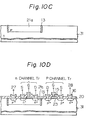
- Figures l0A to 10D are views for explaining a further application of the present invention to CMOS transistors.
- Fig. 10A substantially the same device as shown in Fig. 2B is illustrated.
- Reference numeral 31 denotes an n type semiconductor substrate, 32 silicon nitride layer, 33 molybdenum silicide, 34 a resist layer, and 32A grooves having a submicron width. Boron ions 25 are implanted, and annealing is carried out to form a p type well 21a.
- the grooves 32A are further etched by using the nitride layer 32 as an etching mask.
- the molybdenum silicide may be removed in advance.
- a p channel transistor and an n channel transistor are formed by well known technology.
- reference numerals 27 and 28 denote a p well contact and an n type substrate contact, respectively.
Landscapes
- Element Separation (AREA)
Applications Claiming Priority (4)
| Application Number | Priority Date | Filing Date | Title |
|---|---|---|---|
| JP209173/82 | 1982-11-29 | ||
| JP209172/82 | 1982-11-29 | ||
| JP57209173A JPS5999738A (ja) | 1982-11-29 | 1982-11-29 | 半導体装置の製造方法 |
| JP57209172A JPS5999737A (ja) | 1982-11-29 | 1982-11-29 | 半導体装置の製造方法 |
Publications (3)
| Publication Number | Publication Date |
|---|---|
| EP0113517A2 true EP0113517A2 (de) | 1984-07-18 |
| EP0113517A3 EP0113517A3 (en) | 1986-06-11 |
| EP0113517B1 EP0113517B1 (de) | 1990-01-17 |
Family
ID=26517270
Family Applications (1)
| Application Number | Title | Priority Date | Filing Date |
|---|---|---|---|
| EP83307091A Expired - Lifetime EP0113517B1 (de) | 1982-11-29 | 1983-11-21 | Verfahren zur Herstellung einer Isolationszone |
Country Status (5)
| Country | Link |
|---|---|
| US (1) | US4465532A (de) |
| EP (1) | EP0113517B1 (de) |
| KR (1) | KR860001056B1 (de) |
| CA (1) | CA1204525A (de) |
| DE (1) | DE3381128D1 (de) |
Cited By (4)
| Publication number | Priority date | Publication date | Assignee | Title |
|---|---|---|---|---|
| WO1988005603A1 (fr) * | 1987-01-26 | 1988-07-28 | Commissariat A L'energie Atomique | Procede de fabrication des zones d'isolation electrique d'un circuit integre cmos |
| US5290396A (en) * | 1991-06-06 | 1994-03-01 | Lsi Logic Corporation | Trench planarization techniques |
| US5354706A (en) * | 1993-03-02 | 1994-10-11 | Lsi Logic Corporation | Formation of uniform dimension conductive lines on a semiconductor wafer |
| EP0660389A3 (de) * | 1993-12-27 | 1997-12-29 | Kabushiki Kaisha Toshiba | Verfahren zur Herstellung von Halbleiteranordnungen mit Isolationszonen |
Families Citing this family (21)
| Publication number | Priority date | Publication date | Assignee | Title |
|---|---|---|---|---|
| US4570325A (en) * | 1983-12-16 | 1986-02-18 | Kabushiki Kaisha Toshiba | Manufacturing a field oxide region for a semiconductor device |
| GB8406432D0 (en) * | 1984-03-12 | 1984-04-18 | British Telecomm | Semiconductor devices |
| US4799990A (en) * | 1987-04-30 | 1989-01-24 | Ibm Corporation | Method of self-aligning a trench isolation structure to an implanted well region |
| US5338398A (en) * | 1991-03-28 | 1994-08-16 | Applied Materials, Inc. | Tungsten silicide etch process selective to photoresist and oxide |
| US5248625A (en) | 1991-06-06 | 1993-09-28 | Lsi Logic Corporation | Techniques for forming isolation structures |
| DE4219592C2 (de) * | 1991-06-17 | 2001-12-06 | Gold Star Electronics | Verfahren zur Ausbildung eines Graben-Isolationsbereichs mittels einer Reaktionsschicht |
| FR2683944B1 (fr) * | 1991-11-14 | 1994-02-18 | Sgs Thomson Microelectronics Sa | Procede de gravure d'un sillon profond. |
| US5356828A (en) * | 1993-07-01 | 1994-10-18 | Digital Equipment Corporation | Method of forming micro-trench isolation regions in the fabrication of semiconductor devices |
| US5880033A (en) * | 1996-06-17 | 1999-03-09 | Applied Materials, Inc. | Method for etching metal silicide with high selectivity to polysilicon |
| JP3058112B2 (ja) * | 1997-02-27 | 2000-07-04 | 日本電気株式会社 | 半導体装置およびその製造方法 |
| US5960297A (en) * | 1997-07-02 | 1999-09-28 | Kabushiki Kaisha Toshiba | Shallow trench isolation structure and method of forming the same |
| US6872322B1 (en) | 1997-11-12 | 2005-03-29 | Applied Materials, Inc. | Multiple stage process for cleaning process chambers |
| US6136211A (en) * | 1997-11-12 | 2000-10-24 | Applied Materials, Inc. | Self-cleaning etch process |
| US6322714B1 (en) | 1997-11-12 | 2001-11-27 | Applied Materials Inc. | Process for etching silicon-containing material on substrates |
| US6797188B1 (en) | 1997-11-12 | 2004-09-28 | Meihua Shen | Self-cleaning process for etching silicon-containing material |
| US6527968B1 (en) * | 2000-03-27 | 2003-03-04 | Applied Materials Inc. | Two-stage self-cleaning silicon etch process |
| US6905800B1 (en) | 2000-11-21 | 2005-06-14 | Stephen Yuen | Etching a substrate in a process zone |
| US6852242B2 (en) | 2001-02-23 | 2005-02-08 | Zhi-Wen Sun | Cleaning of multicompositional etchant residues |
| KR100792409B1 (ko) * | 2004-10-12 | 2008-01-09 | 주식회사 하이닉스반도체 | 텅스텐막을 희생 하드마스크로 이용하는 반도체소자 제조방법 |
| US8118946B2 (en) | 2007-11-30 | 2012-02-21 | Wesley George Lau | Cleaning process residues from substrate processing chamber components |
| US8263502B2 (en) * | 2008-08-13 | 2012-09-11 | Synos Technology, Inc. | Forming substrate structure by filling recesses with deposition material |
Family Cites Families (10)
| Publication number | Priority date | Publication date | Assignee | Title |
|---|---|---|---|---|
| DE2251823A1 (de) * | 1972-10-21 | 1974-05-02 | Itt Ind Gmbh Deutsche | Halbleiterelement und herstellungsverfahren |
| US4282647A (en) * | 1978-04-04 | 1981-08-11 | Standard Microsystems Corporation | Method of fabricating high density refractory metal gate MOS integrated circuits utilizing the gate as a selective diffusion and oxidation mask |
| JPS5636143A (en) * | 1979-08-31 | 1981-04-09 | Hitachi Ltd | Manufacture of semiconductor device |
| DE3023410A1 (de) * | 1980-06-23 | 1982-01-07 | Siemens AG, 1000 Berlin und 8000 München | Verfahren zur herstellung von mos-strukturen |
| US4333965A (en) * | 1980-09-15 | 1982-06-08 | General Electric Company | Method of making integrated circuits |
| US4373990A (en) * | 1981-01-08 | 1983-02-15 | Bell Telephone Laboratories, Incorporated | Dry etching aluminum |
| JPS5848936A (ja) * | 1981-09-10 | 1983-03-23 | Fujitsu Ltd | 半導体装置の製造方法 |
| JPS5864044A (ja) * | 1981-10-14 | 1983-04-16 | Toshiba Corp | 半導体装置の製造方法 |
| US4390393A (en) * | 1981-11-12 | 1983-06-28 | General Electric Company | Method of forming an isolation trench in a semiconductor substrate |
| US4422897A (en) * | 1982-05-25 | 1983-12-27 | Massachusetts Institute Of Technology | Process for selectively etching silicon |
-
1983
- 1983-11-04 CA CA000440422A patent/CA1204525A/en not_active Expired
- 1983-11-07 US US06/549,470 patent/US4465532A/en not_active Expired - Fee Related
- 1983-11-14 KR KR1019830005396A patent/KR860001056B1/ko not_active Expired
- 1983-11-21 DE DE8383307091T patent/DE3381128D1/de not_active Expired - Lifetime
- 1983-11-21 EP EP83307091A patent/EP0113517B1/de not_active Expired - Lifetime
Cited By (7)
| Publication number | Priority date | Publication date | Assignee | Title |
|---|---|---|---|---|
| WO1988005603A1 (fr) * | 1987-01-26 | 1988-07-28 | Commissariat A L'energie Atomique | Procede de fabrication des zones d'isolation electrique d'un circuit integre cmos |
| FR2610140A1 (fr) * | 1987-01-26 | 1988-07-29 | Commissariat Energie Atomique | Circuit integre cmos et procede de fabrication de ses zones d'isolation electrique |
| US4889828A (en) * | 1987-01-26 | 1989-12-26 | Commissiriat A L'energie Atomique | Process for the production of electrical isolation zones in a CMOS integrated circuit |
| US5290396A (en) * | 1991-06-06 | 1994-03-01 | Lsi Logic Corporation | Trench planarization techniques |
| US5354706A (en) * | 1993-03-02 | 1994-10-11 | Lsi Logic Corporation | Formation of uniform dimension conductive lines on a semiconductor wafer |
| EP0660389A3 (de) * | 1993-12-27 | 1997-12-29 | Kabushiki Kaisha Toshiba | Verfahren zur Herstellung von Halbleiteranordnungen mit Isolationszonen |
| US5766823A (en) * | 1993-12-27 | 1998-06-16 | Kabushiki Kaisha Toshiba | Method of manufacturing semiconductor devices |
Also Published As
| Publication number | Publication date |
|---|---|
| EP0113517A3 (en) | 1986-06-11 |
| KR860001056B1 (ko) | 1986-08-01 |
| KR840006729A (ko) | 1984-12-01 |
| US4465532A (en) | 1984-08-14 |
| CA1204525A (en) | 1986-05-13 |
| EP0113517B1 (de) | 1990-01-17 |
| DE3381128D1 (de) | 1990-02-22 |
Similar Documents
| Publication | Publication Date | Title |
|---|---|---|
| EP0113517B1 (de) | Verfahren zur Herstellung einer Isolationszone | |
| US5175119A (en) | Method of producing insulated-gate field effect transistor | |
| EP0107416B1 (de) | Verfahren zur Herstellung einer Halbleiteranordnung | |
| US4755477A (en) | Overhang isolation technology | |
| US5777370A (en) | Trench isolation of field effect transistors | |
| EP0782185B1 (de) | Verfahren zur Herstellung einer Halbleitereinrichtung mit einem aus einer Grube herausragenden Isolationsoxid | |
| JPS6240870B2 (de) | ||
| KR100266525B1 (ko) | 반도체장치의제조방법 | |
| GB2129213A (en) | Semiconductor device with dielectric isolation | |
| US4679299A (en) | Formation of self-aligned stacked CMOS structures by lift-off | |
| JPH11145273A (ja) | 半導体装置の製造方法 | |
| US5856227A (en) | Method of fabricating a narrow polycide gate structure on an ultra-thin gate insulator layer | |
| JPH0685412B2 (ja) | 半導体デバイスの製作方法 | |
| JP3039978B2 (ja) | 集積misfetデバイス中に電界分離構造及びゲート構造を形成する方法 | |
| US5612247A (en) | Method for fabricating isolation region for a semiconductor device | |
| US5705440A (en) | Methods of fabricating integrated circuit field effect transistors having reduced-area device isolation regions | |
| US6221745B1 (en) | High selectivity mask oxide etching to suppress silicon pits | |
| US5763316A (en) | Substrate isolation process to minimize junction leakage | |
| JPH10308448A (ja) | 半導体デバイスの隔離膜及びその形成方法 | |
| JP2854019B2 (ja) | Mos型半導体装置の製造方法 | |
| JP2563206B2 (ja) | 半導体集積回路装置の製造方法 | |
| KR0161727B1 (ko) | 반도체 소자의 소자분리방법 | |
| JPH0358430A (ja) | 半導体装置及びその製造方法 | |
| KR0158619B1 (ko) | 반도체 소자의 필드 산화막 제조방법 | |
| JP2002100670A (ja) | 半導体装置及びその製造方法 |
Legal Events
| Date | Code | Title | Description |
|---|---|---|---|
| PUAI | Public reference made under article 153(3) epc to a published international application that has entered the european phase |
Free format text: ORIGINAL CODE: 0009012 |
|
| AK | Designated contracting states |
Designated state(s): DE FR GB |
|
| PUAL | Search report despatched |
Free format text: ORIGINAL CODE: 0009013 |
|
| AK | Designated contracting states |
Kind code of ref document: A3 Designated state(s): DE FR GB |
|
| 17P | Request for examination filed |
Effective date: 19860804 |
|
| 17Q | First examination report despatched |
Effective date: 19880331 |
|
| GRAA | (expected) grant |
Free format text: ORIGINAL CODE: 0009210 |
|
| AK | Designated contracting states |
Kind code of ref document: B1 Designated state(s): DE FR GB |
|
| REF | Corresponds to: |
Ref document number: 3381128 Country of ref document: DE Date of ref document: 19900222 |
|
| ET | Fr: translation filed | ||
| PLBE | No opposition filed within time limit |
Free format text: ORIGINAL CODE: 0009261 |
|
| STAA | Information on the status of an ep patent application or granted ep patent |
Free format text: STATUS: NO OPPOSITION FILED WITHIN TIME LIMIT |
|
| 26N | No opposition filed | ||
| PGFP | Annual fee paid to national office [announced via postgrant information from national office to epo] |
Ref country code: GB Payment date: 19920903 Year of fee payment: 10 |
|
| PGFP | Annual fee paid to national office [announced via postgrant information from national office to epo] |
Ref country code: FR Payment date: 19921127 Year of fee payment: 10 |
|
| PGFP | Annual fee paid to national office [announced via postgrant information from national office to epo] |
Ref country code: DE Payment date: 19930129 Year of fee payment: 10 |
|
| PG25 | Lapsed in a contracting state [announced via postgrant information from national office to epo] |
Ref country code: GB Effective date: 19931121 |
|
| GBPC | Gb: european patent ceased through non-payment of renewal fee |
Effective date: 19931121 |
|
| PG25 | Lapsed in a contracting state [announced via postgrant information from national office to epo] |
Ref country code: FR Effective date: 19940729 |
|
| PG25 | Lapsed in a contracting state [announced via postgrant information from national office to epo] |
Ref country code: DE Effective date: 19940802 |
|
| REG | Reference to a national code |
Ref country code: FR Ref legal event code: ST |