EP0113590A2 - Halbleiter-Zeitschalter - Google Patents
Halbleiter-Zeitschalter Download PDFInfo
- Publication number
- EP0113590A2 EP0113590A2 EP83308013A EP83308013A EP0113590A2 EP 0113590 A2 EP0113590 A2 EP 0113590A2 EP 83308013 A EP83308013 A EP 83308013A EP 83308013 A EP83308013 A EP 83308013A EP 0113590 A2 EP0113590 A2 EP 0113590A2
- Authority
- EP
- European Patent Office
- Prior art keywords
- capacitor
- transistor
- com
- charge
- voltage
- Prior art date
- Legal status (The legal status is an assumption and is not a legal conclusion. Google has not performed a legal analysis and makes no representation as to the accuracy of the status listed.)
- Granted
Links
Images


Classifications
-
- H—ELECTRICITY
- H03—ELECTRONIC CIRCUITRY
- H03K—PULSE TECHNIQUE
- H03K17/00—Electronic switching or gating, i.e. not by contact-making and –breaking
- H03K17/28—Modifications for introducing a time delay before switching
- H03K17/284—Modifications for introducing a time delay before switching in field effect transistor switches
-
- H—ELECTRICITY
- H03—ELECTRONIC CIRCUITRY
- H03K—PULSE TECHNIQUE
- H03K3/00—Circuits for generating electric pulses; Monostable, bistable or multistable circuits
- H03K3/02—Generators characterised by the type of circuit or by the means used for producing pulses
- H03K3/023—Generators characterised by the type of circuit or by the means used for producing pulses by the use of differential amplifiers or comparators, with internal or external positive feedback
- H03K3/0231—Astable circuits
Definitions
- the present invention relates to a semiconductor timer, particularly to a timer circuit formed on a metal oxide semiconductor (MOS) integrated circuit.
- MOS metal oxide semiconductor
- a timer circuit which can set a long time interval.
- an electrically erasable and programmable read only memory (EEPROM) in general requires timer circuits having a time interval of about 10 to 20 msec for erasing and writing operations.
- EEPROM electrically erasable and programmable read only memory
- a capacitor having a very high capacitance for example, about 5600 pF, is required.
- Such a capacitor cannot be formed by a semiconductor, so an external capacitor having a very high capacitance is attached to the integrated circuit.
- this requires the integrated citcuit to have an additional connecting pin, and adds to the work of the manufacturer.
- timer circuits or delay circuits having a time interval of about 3 to 5 msec are required to produce each control pulse.
- timer circuits or delay circuits are formed by a continuously charged or discharged CR circuit consisting of a depletion mode transistor and a MOS capacitor in the MOS integrated circuit, the sizes of the depletion mode transistor and MOS capacitor become very large. Particularly, the size of the MOS capacitor becomes extremely large.
- a semiconductor timer includes a first capacitor: a charge circuit connected to the first capacitor for charging the first capacitor; and a discharge circuit connected to the first capacitor for discharging the first capacitor, and is characterized in that at least one of the charge and discharge circuits includes: a transistor connected to the first capacitor in series and having a gate; and a further capacitor connected to the gate of the transistor, the second capacitor receiving clock pulses and intermittently turning the transistor on in response to the clock pulses so as to charge or discharge the first capacitor.
- a long time interval can be set without increasing the size of the first capacitor.
- the semiconductor timer according to the present invention is useful to set an erasing time.period and writing time period of an EEPROM, or to set a time interval of several msec for another job, especially in a computer system.
- FIG. la illustrates an example of a discharge circuit in a semiconductor timer of the present invention.
- reference symbol T denotes an enhancement mode transistor.
- the drain of the transistor T T is connected to a node N C whereto a first MOS capacitor ( p ot shown) is connected.
- the source of the transistor T T is grounded, and the gate of the transistor T T is connected to one terminal of a second MOS capacitor T C .
- the other terminel of the capacitor T C is connected to a clock generator (not shown) to receive clock pulses from the clock generator.
- the second MOS capacitor T C applies a voltage V G , which is higher than the threshold voltage V th of the enhancement mode transistor T T , to the gate of the enhancement mode transistor T T .
- V G the voltage
- the transistor T T is intermittently turned on to gradually discharge the first MOS capacitor.
- Fig. lb illustrates an equivalent circuit of the discharge circuit shown in Fig. la.
- Equivalent capacitors C TC and C TT correspond to the second MOS capacitor T C and the transistor T T , respectively.
- a relationship between the clock pulses and the voltage V at the gate of the enhancement mode transistor T T is as shown in Fig. lc.
- lb are defined as where ⁇ OX is the relative permittivity of the gate oxide layer, ⁇ O is the permittivity of free space, t OX is the thickness of the gate oxide layer, L TC and L TT are the channel length of the transistor constituting the MOS capacitor T C and of the enhancement mode transistor T T , and W TC and W TT are the channel width of the above tran- sitors.
- the voltage V G at the gate of the enhancement mode transistor T T when the clock pulses become the voltage V CC is defined as Therefore, the voltage V G at the gate of the transistor T T when the clock pulses become the voltage V CC can be easily determined to a voltage higher than the threshold voltage V th of the enhancement mode transistor T T , by designing the channel length L TC and the channel width W TC of the MOS capacitor T C to appropriate values.
- the enhancement mode transistor T T will be turned on when the clock pulses become the voltage V CC , causing the charge in the first MOS capacitor to discharge very slowly. As a result, the size of the first MOS capacitor can be reduced.
- FIG. 2 illustrates an embodiment of the present invention, in which the discharge circuit shown in Fig. la is used.
- reference numeral 10 indicates a discharge circuit
- 20 indicates a charge circuit.
- the discharge and charge circuits 10 and 20 are connected to one terminal (node N C ) of a first MOS capacitor C l .
- the other terminal of the first MOS capacitor C 1 is grounded.
- One terminal of each of the first and second comparators COM 1 and COM 2 is connected to one terminal (node N C ) of the first MOS capacitor C l .
- the first comparator COM l compares the voltage V NC at the node N C with a constant reference voltage of 3 V
- the second comparator COM 2 compares the voltage V NC with a constant reference voltage of 1 V.
- the output terminals of the first and second comparators COM 1 and COM 2 are connected to input terminals of a flip--flop FF of a negative edge trigger type, respectively.
- One output terminal (node N D ) is connected to the discharge circuit 10, and the other output terminal (node N U ) is connected to the charge circuit 20.
- the output of this timer is obtained, for example, from the node N D . It is apparent that the output of the timer may be obtained from the node N U .
- a transistor T 2 for resetting and starting the timer is connected in parallel with the first MOS capacitor C l .
- the discharge circuit 10 comprises a second MOS capacitor C 2 which corresponds to the second MOS capacitor T C shown in Fig. la, an enhancement mode transistor T 3 which corresponds to the transistor T T in Fig. la, a transistor T 4 connected between the gate of the transistor T3 and the earth, and an inverter INV connected between the gate of the transistor T4 and the node N D .
- the charge circuit 20 comprises a transistor T 1 connected between a voltage supply (not shown), for supplying the power supply voltage V CC , and the node N C .
- the gate of the transistor T 1 is connected to the node N U .
- Figure 3 illustrates wave-forms at various points in the embodiment shown in Fig. 2.
- the operation of the embodiment in Fig. 2 will be described with reference to Fig. 3.
- the transistor T 2 is in an on state, the voltage V NC at the node N C , which voltage is equivalent to a voltage across the first MOS capacitor C 1 , is zero (0 V). Therefore, the output of the first comparator COM 1 is "H" level (5 V) and the output of the flip-flop, namely the voltage V NU at the node N U , is also "H” level (5 V). As a result, the transistor T 1 is in an on state. Furthermore, since the voltage V ND at the node N D is "L" level, the transistor T 4 is in an on state and, thus, the transistor T 3 is maintained in an off state during the reset condition.
- the transistor T 1 is turned off and the transistor T 4 is turned off, causing the discharging operation of the first MOS capacitor C 1 to start. Namely, since the transistor T 1 is turned off, the charging operation of the first MOS capacitor C 1 will stop. On the other hand, since the transistor T 4 is off, the voltage V G at the gate of the transistor T 3 momentarily increases each time a clock pulse having a predetermined frequency is applied to the second MOS capacitor C 2 , causing the transistor T 3 to intermittently turn on in response to the clock pulses. Therefore, the first MOS capacitor C 1 is gradually discharged.
- the voltage V NC across the first MOS capacitor C l gradually changes between +3 V and +1 V.
- Figure 4 illustrates a part of another example of the discharge circuit 10 in Fig. 2.
- a transistor T 4 1 is inserted between the second MOS capacitor C 2 and the clock generator (not shown), instead of between the transistor T 4 and the inverter INV in the circuit shown in Fig. 2.
- the transistor T 4 ' is off, and the clock pulses are not applied to the second MOS capacitor C 2 , causing the transistor T 3 (Fig. 2) to be maintained in an off state.
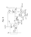
- FIG. 5 illustrates another embodiment of the present invention, in which the discharge circuit 10 in Fig. 4 is used, and a charge circuit 20' different from that shown in the embodiment in Fig. 2 is used. Furthermore, in this embodiment, a high voltage V pp is used for charging the first MOS capacitor C 1 .
- the charge circuit 20' is composed of a charge pump circuit which comprises a third MOS capacitor C 3 and transistors T 5 , T 6 , and T 7 .
- the gate and drain of the transistor T 7 and the source of the transistor T 6 are connected to one terminal of the third MOS capacitor C 3 .
- the other terminal of the third MOS capacitor C 3 is connected to the clock generator (not shown) to receive the clock pulses.
- the source of the transistor T 7 and the gate of the transistor T 6 are connected to the node N C .
- the drain of the transistor T 6 is connected to the source of the transistor T 5 , and the gate and drain of the transistor T 5 are connected to a line for supplying a high voltage V PP of about 19 V.
- Vpp - 3 V a constant reference voltage
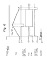
- Figure 6 illustrates waveforms at various points in the embodiment in Fig. 5.
- the operation of the embodiment in Fig. 5 will be explained with reference to Fig. 6..
- the voltage at the gate of the transistor T 7 momentarily increases and thus the transistor T 7 is intermittently turned on, causing a small charge from the line supplying the high voltage Vpp to be pumped into the first MOS capacitor C l . Therefore the first MOS capacitor C 1 is gradually charged, as shown in Fig. 6.
- the first MOS capacitor C 1 is charged by ⁇ Q 1 in response to the clock pulse.
- the transistor T 4 is turned on, causing a discharging operation of the first MOS capacitor C 1 to start.
- the first MOS capacitor C 1 is discharged by ⁇ Q 2 in response to the clock pulse by the discharge circuit 10, and is charged by ⁇ Q 1 in response to the clock pulse by the charge circuit 20'. Since the circuit is designed so that ⁇ Q 2 > ⁇ Q 1 , the first M OS capacitor C 1 in fact is discharged by ⁇ Q 2 - ⁇ Q 1 in response to the clock pulse. Otherwise operation of this embodiment is the same as that of the embodiment shown in Fig. 2.
- a MOS capacitor having a smaller capacitance than that in Fig. 2 can be used for forming the timer having the same time interval. Furthermore, since not only the discharging operation but also the charging operation are executed very slowly, by intermittently turning on the transistor for transmitting charge, a timer having a longer time interval than that in Fig. 2 can be formed.
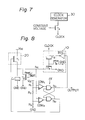
- FIG. 7 illustrates-an example of a circuit for preventing the above problem from occurring.
- a transistor T 8 is inserted between a clock generator 30 and the charge and/or discharge circuits, and a constant voltage of, for example, 4 V, is supplied to the gate of the transistor T 8 . Therefore, the amplitude of the clock pulses is always maintained at a voltage of (4 - V th ) V irrespective of any change in V CC , where V th is a threshold voltage of the transistor T 8 .
- FIG. 8 illustrates a further embodiment of the present invention.
- This embodiment also prevents the above-mentioned problem from occurring.
- variable reference voltages are applied to the first and second comparators COM 1 and COM 2 .
- the variable reference voltges are produced by dividing the power supply voltage V CC by means of resistors R 1 , R 2 , and R 3 connected in series to each other. Therefore, the voltage V NC for switching between the charging and discharging operations changes depending upon the power supply voltage V CC , causing the change in time periods of the charging operation and the discharging operation owing to the charge in the V CC to be reduced. Otherwise, the constitution and operation of the embodiment shown in F ig. 8 are the same.as those of the embodiment in Fig. 2.
Landscapes
- Electronic Switches (AREA)
Applications Claiming Priority (2)
| Application Number | Priority Date | Filing Date | Title |
|---|---|---|---|
| JP57229266A JPS59123320A (ja) | 1982-12-29 | 1982-12-29 | タイマ回路 |
| JP229266/82 | 1982-12-29 |
Publications (3)
| Publication Number | Publication Date |
|---|---|
| EP0113590A2 true EP0113590A2 (de) | 1984-07-18 |
| EP0113590A3 EP0113590A3 (en) | 1986-10-15 |
| EP0113590B1 EP0113590B1 (de) | 1989-11-15 |
Family
ID=16889414
Family Applications (1)
| Application Number | Title | Priority Date | Filing Date |
|---|---|---|---|
| EP83308013A Expired EP0113590B1 (de) | 1982-12-29 | 1983-12-29 | Halbleiter-Zeitschalter |
Country Status (4)
| Country | Link |
|---|---|
| US (1) | US4584494A (de) |
| EP (1) | EP0113590B1 (de) |
| JP (1) | JPS59123320A (de) |
| DE (1) | DE3380865D1 (de) |
Cited By (3)
| Publication number | Priority date | Publication date | Assignee | Title |
|---|---|---|---|---|
| EP0267114A1 (de) * | 1986-11-07 | 1988-05-11 | Thomson Composants Militaires Et Spatiaux | Integrierte Schaltung zur Speicherung und zur vertraulichen Verarbeitung von Informationen, die eine Antibetrugsvorrichtung enthält |
| WO1991009466A1 (en) * | 1989-12-20 | 1991-06-27 | Vlsi Technology, Inc. | Auto-delay gain circuit |
| EP1143617A1 (de) * | 2000-03-31 | 2001-10-10 | STMicroelectronics S.r.l. | Integrierter Generator einer langsamen Spannungsrampe |
Families Citing this family (17)
| Publication number | Priority date | Publication date | Assignee | Title |
|---|---|---|---|---|
| JPS60223321A (ja) * | 1984-04-20 | 1985-11-07 | Toshiba Corp | タイマ回路 |
| US4764694A (en) * | 1987-04-22 | 1988-08-16 | Genrad, Inc. | Interpolating time-measurement apparatus |
| US4812689A (en) * | 1987-08-28 | 1989-03-14 | Hypres, Inc. | Incremental time delay generator |
| JPH01137817A (ja) * | 1987-11-25 | 1989-05-30 | Toshiba Corp | 遅延回路 |
| JP2678115B2 (ja) * | 1992-02-06 | 1997-11-17 | 三菱電機株式会社 | タイマ回路 |
| US5457415A (en) * | 1992-10-30 | 1995-10-10 | International Business Machines Corporation | Charge metering sampling circuit and use thereof in TFT/LCD |
| JP2669591B2 (ja) * | 1992-10-30 | 1997-10-29 | インターナショナル・ビジネス・マシーンズ・コーポレイション | データ・ライン・ドライバ |
| AU7981094A (en) * | 1993-11-09 | 1995-05-29 | Motorola, Inc. | Circuit and method for generating a delayed output signal |
| US5579356A (en) * | 1995-07-28 | 1996-11-26 | Micron Quantum Devices, Inc. | Timer circuit with programmable decode circuitry |
| US5627784A (en) * | 1995-07-28 | 1997-05-06 | Micron Quantum Devices, Inc. | Memory system having non-volatile data storage structure for memory control parameters and method |
| US5629644A (en) * | 1995-07-28 | 1997-05-13 | Micron Quantum Devices, Inc. | Adjustable timer circuit |
| JP2007074794A (ja) * | 2005-09-06 | 2007-03-22 | Rohm Co Ltd | 過電流保護回路、負荷駆動装置、モータ駆動装置、電気機器、電源装置 |
| TWI400884B (zh) * | 2010-05-28 | 2013-07-01 | Macronix Int Co Ltd | 時鐘積體電路 |
| US8922254B2 (en) | 2013-01-29 | 2014-12-30 | Macronix International Co., Ltd. | Drive circuitry compensated for manufacturing and environmental variation |
| US9444462B2 (en) | 2014-08-13 | 2016-09-13 | Macronix International Co., Ltd. | Stabilization of output timing delay |
| US9419596B2 (en) | 2014-09-05 | 2016-08-16 | Macronix International Co., Ltd. | Sense amplifier with improved margin |
| CN113098394B (zh) * | 2021-03-31 | 2025-09-16 | 英韧科技股份有限公司 | 振荡器电路 |
Family Cites Families (9)
| Publication number | Priority date | Publication date | Assignee | Title |
|---|---|---|---|---|
| US3150271A (en) * | 1960-10-06 | 1964-09-22 | Gen Dynamics Corp | Transistor pump circuit with time constant multiplier |
| US3158757A (en) * | 1962-04-23 | 1964-11-24 | Northern Electric Co | Long interval timer circuit |
| US3569842A (en) * | 1968-07-29 | 1971-03-09 | Bendix Corp | Pulse delay circuit |
| JPS49137432U (de) * | 1973-03-26 | 1974-11-26 | ||
| US3893036A (en) * | 1973-07-27 | 1975-07-01 | Tektronix Inc | Precision function generator |
| DE2522463C3 (de) * | 1975-05-16 | 1987-05-07 | Licentia Patent-Verwaltungs-Gmbh, 6000 Frankfurt | Schmittrigger mit zwei Differenzverstärkern |
| US4017747A (en) * | 1975-08-18 | 1977-04-12 | Rca Corporation | First timing circuit controlled by a second timing circuit for generating long timing intervals |
| CH617298A5 (de) * | 1976-05-07 | 1980-05-14 | Ebauches Sa | |
| US4503345A (en) * | 1982-07-02 | 1985-03-05 | Rockwell International Corporation | MOS/LSI Time delay circuit |
-
1982
- 1982-12-29 JP JP57229266A patent/JPS59123320A/ja active Granted
-
1983
- 1983-12-29 DE DE8383308013T patent/DE3380865D1/de not_active Expired
- 1983-12-29 US US06/566,880 patent/US4584494A/en not_active Expired - Lifetime
- 1983-12-29 EP EP83308013A patent/EP0113590B1/de not_active Expired
Cited By (6)
| Publication number | Priority date | Publication date | Assignee | Title |
|---|---|---|---|---|
| EP0267114A1 (de) * | 1986-11-07 | 1988-05-11 | Thomson Composants Militaires Et Spatiaux | Integrierte Schaltung zur Speicherung und zur vertraulichen Verarbeitung von Informationen, die eine Antibetrugsvorrichtung enthält |
| FR2606530A1 (fr) * | 1986-11-07 | 1988-05-13 | Eurotechnique Sa | Circuit integre pour la memorisation et le traitement d'informations de maniere confidentielle comportant un dispositif anti-fraude |
| US4851653A (en) * | 1986-11-07 | 1989-07-25 | Thomson Composants Militaires & Spaciaux | Integrated circuit for memorizing and processing information confidentially, including an anti-fraud device |
| WO1991009466A1 (en) * | 1989-12-20 | 1991-06-27 | Vlsi Technology, Inc. | Auto-delay gain circuit |
| EP1143617A1 (de) * | 2000-03-31 | 2001-10-10 | STMicroelectronics S.r.l. | Integrierter Generator einer langsamen Spannungsrampe |
| US6384645B2 (en) | 2000-03-31 | 2002-05-07 | Stmicroelectronics S.R.L. | Integrated generator of a slow voltage ramp |
Also Published As
| Publication number | Publication date |
|---|---|
| JPS59123320A (ja) | 1984-07-17 |
| JPH035689B2 (de) | 1991-01-28 |
| EP0113590A3 (en) | 1986-10-15 |
| EP0113590B1 (de) | 1989-11-15 |
| US4584494A (en) | 1986-04-22 |
| DE3380865D1 (en) | 1989-12-21 |
Similar Documents
| Publication | Publication Date | Title |
|---|---|---|
| EP0113590B1 (de) | Halbleiter-Zeitschalter | |
| US5670915A (en) | Accurate RC oscillator having peak - to - peak voltage control | |
| US5894239A (en) | Single shot with pulse width controlled by reference oscillator | |
| US5912593A (en) | IC (current-capacitor) precision oscillator having frequency and duty cycle controls | |
| CA1060543A (en) | Boosting circuit | |
| US4407588A (en) | Electronic oscillation counting timer | |
| US4709200A (en) | Power source circuit | |
| US4785262A (en) | Pulse generator producing pulses having a width free from a power voltage and a threshold voltage of an inverter used therein | |
| EP0293045A1 (de) | Integrierter CMOS-Kreis mit Substratvorspannungsregler | |
| US5109163A (en) | Integrated power-on reset circuit | |
| US4736118A (en) | Circuit arrangement to generate squarewave signals with constant duty cycle | |
| EP0055601A2 (de) | Pufferschaltung | |
| US5640118A (en) | Voltage-limiting circuit with hysteresis comparator | |
| US4398100A (en) | Booster circuit | |
| US5386152A (en) | Power-on reset circuit responsive to a clock signal | |
| US4952863A (en) | Voltage regulator with power boost system | |
| US6043749A (en) | Frequency detection circuit | |
| US4370628A (en) | Relaxation oscillator including constant current source and latch circuit | |
| US6373326B1 (en) | Writing circuit | |
| US6483376B1 (en) | Voltage generation circuit of charge pump type, with a self-oscillating control circuit | |
| EP0836129A1 (de) | Spannungsvervielfacher | |
| GB2049327A (en) | Memory read voltage circuitry for adapting EPROMs to circuits employing substrate bias voltage | |
| US4553054A (en) | Power on reset circuit for microprocessor | |
| US4454431A (en) | Semiconductor circuit with a circuit part controlled by a substrate bias | |
| EP1083436B1 (de) | Verfahren und Schaltungsanordnung zum Testen der Anwesenheit von mehreren Versorgungsspannungen in einer integrierten Schaltung |
Legal Events
| Date | Code | Title | Description |
|---|---|---|---|
| PUAI | Public reference made under article 153(3) epc to a published international application that has entered the european phase |
Free format text: ORIGINAL CODE: 0009012 |
|
| AK | Designated contracting states |
Designated state(s): DE FR GB |
|
| PUAL | Search report despatched |
Free format text: ORIGINAL CODE: 0009013 |
|
| AK | Designated contracting states |
Kind code of ref document: A3 Designated state(s): DE FR GB |
|
| 17P | Request for examination filed |
Effective date: 19870313 |
|
| 17Q | First examination report despatched |
Effective date: 19880505 |
|
| GRAA | (expected) grant |
Free format text: ORIGINAL CODE: 0009210 |
|
| AK | Designated contracting states |
Kind code of ref document: B1 Designated state(s): DE FR GB |
|
| ET | Fr: translation filed | ||
| REF | Corresponds to: |
Ref document number: 3380865 Country of ref document: DE Date of ref document: 19891221 |
|
| PLBE | No opposition filed within time limit |
Free format text: ORIGINAL CODE: 0009261 |
|
| STAA | Information on the status of an ep patent application or granted ep patent |
Free format text: STATUS: NO OPPOSITION FILED WITHIN TIME LIMIT |
|
| 26N | No opposition filed | ||
| PGFP | Annual fee paid to national office [announced via postgrant information from national office to epo] |
Ref country code: FR Payment date: 19971209 Year of fee payment: 15 |
|
| PGFP | Annual fee paid to national office [announced via postgrant information from national office to epo] |
Ref country code: GB Payment date: 19971222 Year of fee payment: 15 |
|
| PGFP | Annual fee paid to national office [announced via postgrant information from national office to epo] |
Ref country code: DE Payment date: 19980105 Year of fee payment: 15 |
|
| PG25 | Lapsed in a contracting state [announced via postgrant information from national office to epo] |
Ref country code: GB Free format text: LAPSE BECAUSE OF NON-PAYMENT OF DUE FEES Effective date: 19981229 |
|
| GBPC | Gb: european patent ceased through non-payment of renewal fee |
Effective date: 19981229 |
|
| PG25 | Lapsed in a contracting state [announced via postgrant information from national office to epo] |
Ref country code: FR Free format text: LAPSE BECAUSE OF NON-PAYMENT OF DUE FEES Effective date: 19990831 |
|
| REG | Reference to a national code |
Ref country code: FR Ref legal event code: ST |
|
| PG25 | Lapsed in a contracting state [announced via postgrant information from national office to epo] |
Ref country code: DE Free format text: LAPSE BECAUSE OF NON-PAYMENT OF DUE FEES Effective date: 19991001 |