EP0114061A2 - Dispositif semi-conducteur comportant des structures CMOS - Google Patents
Dispositif semi-conducteur comportant des structures CMOS Download PDFInfo
- Publication number
- EP0114061A2 EP0114061A2 EP84100232A EP84100232A EP0114061A2 EP 0114061 A2 EP0114061 A2 EP 0114061A2 EP 84100232 A EP84100232 A EP 84100232A EP 84100232 A EP84100232 A EP 84100232A EP 0114061 A2 EP0114061 A2 EP 0114061A2
- Authority
- EP
- European Patent Office
- Prior art keywords
- type
- conductivity
- channel mos
- mos transistor
- semiconductor device
- Prior art date
- Legal status (The legal status is an assumption and is not a legal conclusion. Google has not performed a legal analysis and makes no representation as to the accuracy of the status listed.)
- Withdrawn
Links
Images



Classifications
-
- H—ELECTRICITY
- H10—SEMICONDUCTOR DEVICES; ELECTRIC SOLID-STATE DEVICES NOT OTHERWISE PROVIDED FOR
- H10D—INORGANIC ELECTRIC SEMICONDUCTOR DEVICES
- H10D48/00—Individual devices not covered by groups H10D1/00 - H10D44/00
- H10D48/387—Devices controllable only by the variation of applied heat
-
- H—ELECTRICITY
- H10—SEMICONDUCTOR DEVICES; ELECTRIC SOLID-STATE DEVICES NOT OTHERWISE PROVIDED FOR
- H10D—INORGANIC ELECTRIC SEMICONDUCTOR DEVICES
- H10D84/00—Integrated devices formed in or on semiconductor substrates that comprise only semiconducting layers, e.g. on Si wafers or on GaAs-on-Si wafers
- H10D84/80—Integrated devices formed in or on semiconductor substrates that comprise only semiconducting layers, e.g. on Si wafers or on GaAs-on-Si wafers characterised by the integration of at least one component covered by groups H10D12/00 or H10D30/00, e.g. integration of IGFETs
- H10D84/82—Integrated devices formed in or on semiconductor substrates that comprise only semiconducting layers, e.g. on Si wafers or on GaAs-on-Si wafers characterised by the integration of at least one component covered by groups H10D12/00 or H10D30/00, e.g. integration of IGFETs of only field-effect components
- H10D84/83—Integrated devices formed in or on semiconductor substrates that comprise only semiconducting layers, e.g. on Si wafers or on GaAs-on-Si wafers characterised by the integration of at least one component covered by groups H10D12/00 or H10D30/00, e.g. integration of IGFETs of only field-effect components of only insulated-gate FETs [IGFET]
- H10D84/85—Complementary IGFETs, e.g. CMOS
- H10D84/858—Complementary IGFETs, e.g. CMOS comprising a P-type well but not an N-type well
Definitions
- the present invention relates to a CMOS type integrated circuit, and particularly to a semiconductor device which operates at very high speeds and which can be highly integrated.
- CMOS integrated circuit consisting of n-channel MOS transistors (NMOS) and p-channel MOS transistors (.PMOS)
- NMOS n-channel MOS transistors
- PMOS p-channel MOS transistors
- the carrier mobility remains constant, and the operation speed can be increased only by reducing the size of the device in the manufacturing process.
- NMOS n-channel MOS transistors
- .PMOS p-channel MOS transistors
- Fig. 1 is a section view of the structure of a typical CMOS device, in which a p-channel MOS transistor Ql consists of a gate 1, a gate oxide film 2, a source 3 and a drain 4 of p +- diffusion layer, which are formed in an n-well region 5.
- An n-channel MOS transistor Q2 consists of a gate 1, a gate oxide film 2, a source 6 and a drain 7 of n-diffusion layer, which are formed in a p-well region 8.
- a junction field-effect transistor Q3 has a p-well 8 with an open hole that serves as a gate, with a drain 9 and a source 11 of n - diffusion layer formed on the hole.
- a parasitic n-channel MOS transistor or a parasitic p-channel MOS transistor is formed.
- the parasitic MOS transistor hinders the electric isolation between them.
- the p-channel MOS transistor and the n-channel MOS transistor are formed close to each other, the latch-up phenomenon develops due to a parasitic bipolar transistor that is formed in the well region and in the substrate. Because of these reasons, it is difficult to reduce the size of the elements. To increase the operation speed of CMOS devices, however,
- the object of the present invention is to provide a CMOS-type semiconductor integrated circuit which operates at very high speeds, which can be highly integrated and which consumes little electric power.
- CMOS structure in which a field-effect transistor with source and drain regions of a first type of electric conductivity, and a field-effect transistor with source and drain regions of a second type of electric conductivity are formed in the regions having different conductivity types in a silicon substrate.
- a semiconductor integrated circuit in which a first field-effect transistor with source and drain regions of a first type of conductivity, and a second field-effect transistor with source and drain regions of a second type of conductivity, are formed in the regions having the same conductivity type in a silicon substrate.
- a well region of a second type of conductivity having an opening is provided on the surface of a silicon substrate of a first type of conductivity having a first highly doped region in the bottom portion thereof, a second highly doped region of the first type of conductivity in the opening, a lightly doped region sandwiched between the first and second highly doped regions exhibits a high resistance over a temperature range in which the impurities freeze out, and an electric current is supplied to an element in the well region via the high resistance.
- CMOS type semiconductor integrated circuit consisting of an n-channel MOS transistor and a p-channel MOS transistor is cooled to a very low temperature, and electric power, and input signals are applied thereto, and output signals are taken out therefrom.
- the present invention operates the CMOS type semiconductor integrated circuit at a very low temperature.
- the integrated circuit can be cooled by cooling means employed for Josephson elements.
- Figs. 2A and 2B illustrate a first embodiment according to the present invention.
- a CMOS type inverter circuit consisting of a p-channel MOS transistor Ql and an n-channel MOS transistor Q2 as shown in Fig. 2A, is formed based upon a so-called CMOS structure shown in Fig. 2B. That is, the. p-channel MOS transistor is composed of p + - type regions 205, 206 and a gate electrode 208 on the surface region of an n-type silicon substrate 201.
- the n-channel MOS transistor is composed of n +- type regions 203, 204 in a p-type well region, and a gate electrode 207.
- Gate insulating films 200 are composed of SiO 2 or the like.
- CMOS structure can also be realized by forming an n-type well region 210 in a p-type silicon substrate 209 as shown in Fig. 2C.
- Figs. 3A and 3B show an embodiment consisting of a CMOS type circuit of the transistors Ql, Q2, and a circuit formed by coupling a junction field-effect transistor Q3 and an MOS transistor Q4.
- a p-type well region 202' has an opening at which the surface of the n-type silicon substrate is exposed, and an n -type region 211 is formed on the surface of the opening.
- a junction transistor is formed with the n +- type region 212 formed on the surface of the n-type silicon substrate 201 serving as the drain, the n +- type region 211 serving as the source, and the p-type well region 2Q2' serving as a junction-type gate.
- junction transistor and the n-channel MOS transistor in the p-type well region 202' are coupled together to obtain the circuit composed of transistors Q3 and Q4 of Fig. 3A.
- Other reference numerals denote the same portions as those of Fig. 2B.
- the circuit of this embodiment is also operated at a temperature lower than 100 a K.
- CMOS devices The latch-up phenomenon that takes place in CMOS devices is caused by the thyristor action of a parasitic bipolar transistor that forms in the well region and in the substrate. So far, the n-channel MOS transistor and the p-channel MOS transistor had been formed relatively far apart to decrease the gain ß of the parasitic bipolar transistor, thus sacrificing a degree of integration.
- Fig. 4 shows experimental data on the temperature dependency of the gain ß of the parasitic bipolar transistor. As the temperature decreases from 300°K to 77°K, the gain ß decreases to 1/60. As the temperature further decreases to 4.2°K, the gain ß decreases to 1/520. It will therefore be apparent that the parasitic bipolar transistor ceases to contribute to developing latch-up phenomenon at very low temperatures.
- Fig. 5 shows experimental data on the sheet resistance of the well region produced by the parasitic bipolar transistor.
- the resistance decreases to 1/3.8. Due to the decreased resistance, the bias voltage applied to the parasitic bipolar transistor is reduced and the gain ß decreases. Therefore, the latch-up phenomenon takes place less.
- the resistance becomes greater than 10 megaohms/ ⁇ due to the freeze-out of impurities, and the latch-up current does not flow any more. Further, the gain ⁇ of the parasitic bipolar transistor decreases and the latch-up phenomenon does not develop. It was also found that a similar temperature dependency exists for the sheet resistance of the substrate.
- Fig. 6 shows the results of the measurements on the temperature dependency of the'latch-up phenomenon.
- the ordinate represents a DC injection current that is required to develop the latch-up phenomenon.
- an increasing current must be supplied to the parasitic bipolar transistor to latch-up it. Namely, the latch-up phenomenon develops less easily.
- the latch-up phenomenon did not take place at 77°K even when the injection current that was supplied at 300°K was increased by ten thousand times. It is obvious that the problem of latch-up diminishes at very low temperatures, and virtually disappears at temperatures lower than 100°K.
- the n-channel MOS transistor and the p-channel MOS transistor can be formed close to each other, increasing the degree of integration.
- Isolation of the MOS transistors also plays an important role in the forming of highly integrated CMOS devices.
- Fig. 7 is a section view of a CMOS device according to an embodiment of the present invention which includes parasitic MOS transistors.
- symbols Q4 and Q6 denoteactive p-channel MOS transistors
- Q5 denotes a parasitic p-channel MOS transistor
- Q7 and Q9 denote active n-channel MOS transistors
- Q8 denotes a parasitic n-channel MOS transistor.
- the active MOS transistors use gates 1 and gate oxide films 2
- the p-channel MOS transistors use p -type diffusion layers 3, 4, 12 and 13 as sources and drains
- the n-channel MOS transistors use n + -type diffusion layers 6, 7, 14, 15 as sources and drains.
- the p-channel MOS transistors Q4 and Q6 are formed in the n-type well region which has a higher impurity concentration than the n - -type substrate.
- Gates of the parasitic MOS transistors are formed by metal interconnection lines 16, and gate oxide films are formed by field oxide films 17. In order to increase the degree of integration, electric isolation must be obtained without increasing the channel lengths l 1 , l 2 of the parasitic MOS transistors.
- Fig. 8 shows the results of the measurements on the threshold voltages of the active MOS transistors and of the parasitic MOS transistors. Threshold voltages of the parasitic n-channel MOS transistor and parasitic p-channel MOS transistor increase with lower temperatures as compared with the values at 300°K, and become greater than the difference between the threshold voltages of the active MOS transistors. That is, there is no problem with electric isolation even when the device is operated at low temperatures.
- Fig. 9 shows the results of the measurements on the temperature dependency of the operational speed and power dissipation of a CMOS inverter.
- the operation speed is 1.6 times higher when the device is operated at 77°K than at 300°K, and 3 times higher at 4.2°K than at 300°K.
- the threshold voltage increases with the decrease in temperature. Therefore, the power dissipation increases little with increased operation speed.
- the CMOS devices When operated at low temperatures, the CMOS devices feature very high speed with low electric power consumption. Even when the.threshold voltage is set to a small value, it increases when the device is operated at low temperatures, and high-speed operation can be realized.
- Fig. 10A shows a further embodiment of the present invention according to which the CMOS device is formed directly in the n-type substrate 10 instead of being formed in the well region.
- Both the p-channel MOS transistor Ql and the n-channel MOS transistor Q2 are formed in the n-type silicon substrate 10. Since the substrate 10 has a low impurity concentration (smaller than 1 0 17 cm -3 ), the impurities freeze out at temperatures lower than 20°K and the substrate exhibits a high resistance (greater than 1 gigaohms/ ⁇ ). Therefore, electric isolation is obtained for the CMOS device of Fig. 10A. The electric isolation l 3 can also be obtained.between the p-channel MOS transistor and the n-channel MOS transistor of Fig.
- the substrate 10 since the substrate 10 exhibits increased resistance. Therefore, this structure is effective for increasing the degree of integration.
- the increased resistance helps decrease the gate capacitance, junction capacitance and capacitance of interconnection lines, that are parasitic in the substrate 10, and, therefore helps increase the operation speed.
- the increased resistance further helps eliminate the formation of parasitic bipolar transistors and the latch-up phenomenon. In the pn junction, the leakage current decreases to reduce electric power consumption. When operated at low temperatures, carrier mobility increases, accomplishing high-speed operation.
- the conductivity types of each of the portions of Fig. 10A may be reversed, and the p-channel MOS transistor and the n-channel MOS transistor may be formed in the p-type silicon substrate.
- the device is operated at a temperature lower than 20°K.
- Fig. 11A shows still another embodiment of the present invention.
- a common p-type well region 8 having a low impurity concentration smaller than 10 17 cm -3 ) is formed for the n-channel MOS transistor and the p-channel MOS transistor in the substrate 10 of Fig. 10A.
- the impurities freeze out and the p-type well region 8 and the substrate 10 exhibit high resistances.
- Provision of the p-type well region 8 helps isolate more reliably the MOS transistors from the substrate 10 than in the case of Fig. 10A, and further reduces parasitic capacitance relative to the substrate-10, enabling the operation speed to be correspondingly increased.
- Fig. 11A shows still another embodiment of the present invention.
- a common p-type well region 8 having a low impurity concentration (smaller than 10 17 cm -3 ) is formed for the n-channel MOS transistor and the p-channel MOS transistor in the substrate 10 of Fig. 10A.
- the operation speed is increased owing to increased carrier mobility
- the degree of integration is raised owing to simplified isolation construction
- the consumption of electric power is reduced owing to reduction in the leakage current in the pn junction.
- the conductivity types of each of the portions may be reversed.
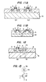
- Fig. 12 shows a yet further embodiment employing a high resistance 19 (greater than 1 megaohms) which can be highly integrated at temperatures lower than 20°K.
- a p-type well region 8 with a hole is formed in the upper portion of the substrate 10 having a low impurity concentration (smaller than 10 17 cm -3 ).
- One side thereof is connected to a terminal of n +- type layer 4 and the other side to a terminal of n +- type layer 18 formed under the hole and under the p-type well region 8, thereby constituting a high resistance 19.
- the impurities in the substrate 10 are frozen out, and a high resistance is produced between the terminal 4 and the terminal 18.
- This construction resembles a junction field-effect transistor.
- a junction field-effect transistor would not operate.
- a high resistance is realized by using a polycrystalline silicon that is generally used for producing a high resistance at ordinary temperatures. The high resistance therefore assumes lateral construction.
- the high resistance 19 is formed in the vertical construction and is effective for increasing the degree of integration.
- Fig. 15 shows an example in which one terminal 4 of the high resistance 19 is connected to the drain 4 of the n-channel MOS transistor Q2. In this case, the transistor Q2 and the high resistance 19 can be formed close to each other.
- Fig. 13 is a circuit equivalent to Fig. 12.
- the high resistance shown in Fig. 12 can be employed in the CMOS structure described earlier.
- Fig. l4A shows an example
- Fig. l4B shows the case when the conductivity types of each of the portions of Fig. l4A are reversed.
- a flip-flop circuit is formed by combining two sets of high resistors 19 from Fig. 12 and n-channel MOS transistors Q2.
- the high resistances 19, 19' assume vertical construction, and a terminal 18 serves as a common terminal in the substrate, contributing to increasing the degree of integration. At temperatures lower than 20°K, the device works as a static memory cell which consumes little electric power.
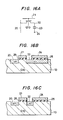
- Fig. 16A shows an embodiment in which the present invention is adapted to a dynamic memory cell, the cell being composed of a storage capacitance 23 and a transfer MOS transistor Q10.
- An electric charge stored in a storage node 22 is sent to a data line by a transfer MOS transistor that is addressed by a word line 21 and a data line 20, and is detected and amplified by a sense amplifier.
- the storage capacitance may be established by a gate 24, an n +- type diffusion layer 22 and a thin oxide film as shown in Fig. l6B, or may be established between the channel and the gate of the n-channel MOS transistor, which consists of a source 22 of an n +- type diffusion layer and a gate 24 as shown in Fig. 16C.
Landscapes
- Metal-Oxide And Bipolar Metal-Oxide Semiconductor Integrated Circuits (AREA)
- Semiconductor Memories (AREA)
- Logic Circuits (AREA)
Applications Claiming Priority (2)
| Application Number | Priority Date | Filing Date | Title |
|---|---|---|---|
| JP2218/83 | 1983-01-12 | ||
| JP58002218A JPS59127857A (ja) | 1983-01-12 | 1983-01-12 | 半導体装置 |
Publications (2)
| Publication Number | Publication Date |
|---|---|
| EP0114061A2 true EP0114061A2 (fr) | 1984-07-25 |
| EP0114061A3 EP0114061A3 (fr) | 1985-10-09 |
Family
ID=11523215
Family Applications (1)
| Application Number | Title | Priority Date | Filing Date |
|---|---|---|---|
| EP84100232A Withdrawn EP0114061A3 (fr) | 1983-01-12 | 1984-01-11 | Dispositif semi-conducteur comportant des structures CMOS |
Country Status (3)
| Country | Link |
|---|---|
| EP (1) | EP0114061A3 (fr) |
| JP (1) | JPS59127857A (fr) |
| CA (1) | CA1205571A (fr) |
Cited By (3)
| Publication number | Priority date | Publication date | Assignee | Title |
|---|---|---|---|---|
| EP0305937A1 (fr) * | 1987-08-31 | 1989-03-08 | National Semiconductor Corporation | Protection MOS d'entrée/sortie utilisant le concept de circuit à corps commutable |
| EP0362961A1 (fr) * | 1988-10-03 | 1990-04-11 | Interuniversitair Microelektronica Centrum Vzw | Procédé pour le fonctionnement d'une structure MOS et structure MOS dans ce but |
| WO1999004607A1 (fr) * | 1997-07-18 | 1999-01-28 | Flame Spray Spa | Appareil permettant d'appliquer des revetements de protection au moyen de la technique du plasma |
Families Citing this family (2)
| Publication number | Priority date | Publication date | Assignee | Title |
|---|---|---|---|---|
| CN104601164A (zh) * | 2015-02-04 | 2015-05-06 | 苏州大学 | 一种基于3只mos管设计的反相器和滤波电路 |
| JP6856640B2 (ja) * | 2016-06-20 | 2021-04-07 | 三菱電機株式会社 | 並列駆動回路 |
Family Cites Families (3)
| Publication number | Priority date | Publication date | Assignee | Title |
|---|---|---|---|---|
| US3493824A (en) * | 1967-08-31 | 1970-02-03 | Gen Telephone & Elect | Insulated-gate field effect transistors utilizing a high resistivity substrate |
| JPS5939904B2 (ja) * | 1978-09-28 | 1984-09-27 | 株式会社東芝 | 半導体装置 |
| DE2947311C2 (de) * | 1978-11-24 | 1982-04-01 | Hitachi, Ltd., Tokyo | Integrierte Halbleiterschaltung |
-
1983
- 1983-01-12 JP JP58002218A patent/JPS59127857A/ja active Granted
-
1984
- 1984-01-11 EP EP84100232A patent/EP0114061A3/fr not_active Withdrawn
- 1984-01-12 CA CA000445161A patent/CA1205571A/fr not_active Expired
Cited By (3)
| Publication number | Priority date | Publication date | Assignee | Title |
|---|---|---|---|---|
| EP0305937A1 (fr) * | 1987-08-31 | 1989-03-08 | National Semiconductor Corporation | Protection MOS d'entrée/sortie utilisant le concept de circuit à corps commutable |
| EP0362961A1 (fr) * | 1988-10-03 | 1990-04-11 | Interuniversitair Microelektronica Centrum Vzw | Procédé pour le fonctionnement d'une structure MOS et structure MOS dans ce but |
| WO1999004607A1 (fr) * | 1997-07-18 | 1999-01-28 | Flame Spray Spa | Appareil permettant d'appliquer des revetements de protection au moyen de la technique du plasma |
Also Published As
| Publication number | Publication date |
|---|---|
| EP0114061A3 (fr) | 1985-10-09 |
| JPS59127857A (ja) | 1984-07-23 |
| JPH0430188B2 (fr) | 1992-05-21 |
| CA1205571A (fr) | 1986-06-03 |
Similar Documents
| Publication | Publication Date | Title |
|---|---|---|
| US6924560B2 (en) | Compact SRAM cell with FinFET | |
| US5557231A (en) | Semiconductor device with improved substrate bias voltage generating circuit | |
| US6963100B2 (en) | Semiconductor device having gate electrode in which depletion layer can be generated | |
| JP2001352077A (ja) | Soi電界効果トランジスタ | |
| JP2953482B2 (ja) | Cmos集積回路 | |
| EP0426174B1 (fr) | Circuit intégré semi-conducteur | |
| JPS6072243A (ja) | 半導体集積回路装置 | |
| HK79493A (en) | Integrated circuit of the complementary technique having a substrate bias generator | |
| US5990521A (en) | Semiconductor device and method of producing the same | |
| EP0114061A2 (fr) | Dispositif semi-conducteur comportant des structures CMOS | |
| US5635753A (en) | Integrated circuit | |
| US7208798B2 (en) | Semiconductor device with an enhancement type field effect transistor in which threshold voltage is dependent upon substrate bias voltage | |
| US5422507A (en) | Electrical isolation in integrated circuits | |
| JPH0695528B2 (ja) | 半導体装置の製造方法 | |
| US6285227B1 (en) | Latch ratio circuit with plural channels | |
| US6713815B2 (en) | Semiconductor device with transistors that convert a voltage difference into a drain current difference | |
| HK59996A (en) | Integrated circuit with anti-''latch-up'' circuit obtained using complementary mos circuit technology | |
| US6677802B2 (en) | Method and apparatus for biasing body voltages | |
| JPS6244861B2 (fr) | ||
| JPS61218165A (ja) | 半導体記憶装置及び製造方法 | |
| US5936290A (en) | Semiconductor device having an insulated gate field effect transistor and a well spaced from the channel region of the insulated gate field effect transistor | |
| JPS5943828B2 (ja) | Mos形集積回路の製造方法 | |
| JP3067678B2 (ja) | 半導体装置 | |
| JPH0147902B2 (fr) | ||
| JPH0243347B2 (fr) |
Legal Events
| Date | Code | Title | Description |
|---|---|---|---|
| PUAI | Public reference made under article 153(3) epc to a published international application that has entered the european phase |
Free format text: ORIGINAL CODE: 0009012 |
|
| 17P | Request for examination filed |
Effective date: 19840116 |
|
| AK | Designated contracting states |
Designated state(s): DE FR GB NL |
|
| PUAL | Search report despatched |
Free format text: ORIGINAL CODE: 0009013 |
|
| AK | Designated contracting states |
Designated state(s): DE FR GB NL |
|
| 17Q | First examination report despatched |
Effective date: 19870612 |
|
| STAA | Information on the status of an ep patent application or granted ep patent |
Free format text: STATUS: THE APPLICATION HAS BEEN WITHDRAWN |
|
| 18W | Application withdrawn |
Withdrawal date: 19871016 |
|
| RIN1 | Information on inventor provided before grant (corrected) |
Inventor name: KOMORIYA, GOH Inventor name: HANAMURA, SYOJI Inventor name: AOKI, MASAAKI Inventor name: MINATO, OSAMU Inventor name: MASUHARA, TOSHIAKI |