EP0116010B1 - Anordnung zum Schutz gegen Funkensprühen eines kapillaren Teiles das zum Schweissen von Drähten in einem Halbleiterelement dient - Google Patents
Anordnung zum Schutz gegen Funkensprühen eines kapillaren Teiles das zum Schweissen von Drähten in einem Halbleiterelement dient Download PDFInfo
- Publication number
- EP0116010B1 EP0116010B1 EP84810001A EP84810001A EP0116010B1 EP 0116010 B1 EP0116010 B1 EP 0116010B1 EP 84810001 A EP84810001 A EP 84810001A EP 84810001 A EP84810001 A EP 84810001A EP 0116010 B1 EP0116010 B1 EP 0116010B1
- Authority
- EP
- European Patent Office
- Prior art keywords
- capillary
- fact
- coating layer
- capillary member
- wire
- Prior art date
- Legal status (The legal status is an assumption and is not a legal conclusion. Google has not performed a legal analysis and makes no representation as to the accuracy of the status listed.)
- Expired
Links
Images
Classifications
-
- B—PERFORMING OPERATIONS; TRANSPORTING
- B23—MACHINE TOOLS; METAL-WORKING NOT OTHERWISE PROVIDED FOR
- B23K—SOLDERING OR UNSOLDERING; WELDING; CLADDING OR PLATING BY SOLDERING OR WELDING; CUTTING BY APPLYING HEAT LOCALLY, e.g. FLAME CUTTING; WORKING BY LASER BEAM
- B23K20/00—Non-electric welding by applying impact or other pressure, with or without the application of heat, e.g. cladding or plating
- B23K20/002—Non-electric welding by applying impact or other pressure, with or without the application of heat, e.g. cladding or plating specially adapted for particular articles or work
- B23K20/004—Wire welding
- B23K20/005—Capillary welding
- B23K20/007—Ball bonding
-
- H—ELECTRICITY
- H10—SEMICONDUCTOR DEVICES; ELECTRIC SOLID-STATE DEVICES NOT OTHERWISE PROVIDED FOR
- H10W—GENERIC PACKAGES, INTERCONNECTIONS, CONNECTORS OR OTHER CONSTRUCTIONAL DETAILS OF DEVICES COVERED BY CLASS H10
- H10W72/00—Interconnections or connectors in packages
- H10W72/01—Manufacture or treatment
- H10W72/015—Manufacture or treatment of bond wires
- H10W72/01551—Changing the shapes of bond wires
-
- H—ELECTRICITY
- H10—SEMICONDUCTOR DEVICES; ELECTRIC SOLID-STATE DEVICES NOT OTHERWISE PROVIDED FOR
- H10W—GENERIC PACKAGES, INTERCONNECTIONS, CONNECTORS OR OTHER CONSTRUCTIONAL DETAILS OF DEVICES COVERED BY CLASS H10
- H10W72/00—Interconnections or connectors in packages
- H10W72/071—Connecting or disconnecting
- H10W72/0711—Apparatus therefor
- H10W72/07141—Means for applying energy, e.g. ovens or lasers
-
- H—ELECTRICITY
- H10—SEMICONDUCTOR DEVICES; ELECTRIC SOLID-STATE DEVICES NOT OTHERWISE PROVIDED FOR
- H10W—GENERIC PACKAGES, INTERCONNECTIONS, CONNECTORS OR OTHER CONSTRUCTIONAL DETAILS OF DEVICES COVERED BY CLASS H10
- H10W72/00—Interconnections or connectors in packages
- H10W72/071—Connecting or disconnecting
- H10W72/075—Connecting or disconnecting of bond wires
- H10W72/07511—Treating the bonding area before connecting, e.g. by applying flux or cleaning
-
- H—ELECTRICITY
- H10—SEMICONDUCTOR DEVICES; ELECTRIC SOLID-STATE DEVICES NOT OTHERWISE PROVIDED FOR
- H10W—GENERIC PACKAGES, INTERCONNECTIONS, CONNECTORS OR OTHER CONSTRUCTIONAL DETAILS OF DEVICES COVERED BY CLASS H10
- H10W72/00—Interconnections or connectors in packages
- H10W72/071—Connecting or disconnecting
- H10W72/075—Connecting or disconnecting of bond wires
- H10W72/07531—Techniques
- H10W72/07532—Compression bonding, e.g. thermocompression bonding
- H10W72/07533—Ultrasonic bonding, e.g. thermosonic bonding
-
- H—ELECTRICITY
- H10—SEMICONDUCTOR DEVICES; ELECTRIC SOLID-STATE DEVICES NOT OTHERWISE PROVIDED FOR
- H10W—GENERIC PACKAGES, INTERCONNECTIONS, CONNECTORS OR OTHER CONSTRUCTIONAL DETAILS OF DEVICES COVERED BY CLASS H10
- H10W72/00—Interconnections or connectors in packages
- H10W72/50—Bond wires
- H10W72/551—Materials of bond wires
- H10W72/552—Materials of bond wires comprising metals or metalloids, e.g. silver
- H10W72/5522—Materials of bond wires comprising metals or metalloids, e.g. silver comprising gold [Au]
-
- H—ELECTRICITY
- H10—SEMICONDUCTOR DEVICES; ELECTRIC SOLID-STATE DEVICES NOT OTHERWISE PROVIDED FOR
- H10W—GENERIC PACKAGES, INTERCONNECTIONS, CONNECTORS OR OTHER CONSTRUCTIONAL DETAILS OF DEVICES COVERED BY CLASS H10
- H10W72/00—Interconnections or connectors in packages
- H10W72/50—Bond wires
- H10W72/551—Materials of bond wires
- H10W72/552—Materials of bond wires comprising metals or metalloids, e.g. silver
- H10W72/5524—Materials of bond wires comprising metals or metalloids, e.g. silver comprising aluminium [Al]
-
- H—ELECTRICITY
- H10—SEMICONDUCTOR DEVICES; ELECTRIC SOLID-STATE DEVICES NOT OTHERWISE PROVIDED FOR
- H10W—GENERIC PACKAGES, INTERCONNECTIONS, CONNECTORS OR OTHER CONSTRUCTIONAL DETAILS OF DEVICES COVERED BY CLASS H10
- H10W72/00—Interconnections or connectors in packages
- H10W72/50—Bond wires
- H10W72/551—Materials of bond wires
- H10W72/552—Materials of bond wires comprising metals or metalloids, e.g. silver
- H10W72/5525—Materials of bond wires comprising metals or metalloids, e.g. silver comprising copper [Cu]
Definitions
- the present invention relates to the capillary members used for welding the wires which connect the contact pads of a chip to the poles of its envelope or support, and it relates to the protection of these members against sparking and carbon deposits resulting from the electric arc.
- connection wires are soldered to the contact pads of the chip and to the output terminals of its envelope.
- these connections are made using very fine wires, the diameter of which, in common semiconductor elements, is of the order of 25 microns. This diameter can however go up to 500 microns in high power elements.
- connection wires are generally made of gold or aluminum.
- thermocompression of a smooth gold ball and solder point (2) thermosonic fixation of a smooth gold ball and solder point and (3) fixation thermosonic or ultrasonic of a smooth aluminum ball and solder point.
- the wire after being welded to the contact patch of the chip and to the output terminal of its envelope, is broken in line with the last weld, then a ball is formed at its end for the next connection.
- the ball is formed by means of a charcoal electric arc, as described below.
- the weaker hydrogen arc was used. With the latter, the main cause of wear of the capillary organs was due to abrasion. The lifetime of such a body, made of ceramic, was commonly one million welds. By switching to a charcoal arc, however, this lifespan fell below half a million solders. The main reason for this fall, however, was no longer abrasion, but, on the one hand, sparking, which damages the end of the capillary organ, and, on the other hand, carbon deposits, which form inside the duct of this organ.
- capillary members are already known for the welding of wires on semiconductor elements, which comprise a body of insulating material, the outer surface of which has a frustoconical section adjacent to an upper cylindrical section and terminated at its lower end by a rounded face, this body having a through axial duct formed of two cylindrical sections, respectively upper and lower, connected to each other by a frustoconical middle section and in which passes the welding wire, but which have the aforementioned drawbacks.
- capillary members for welding wires are also known, for example from document JP-A-5 710 944, but which are designed differently in that they comprise a body essentially formed of a conductive material and whose internal wall of the axial duct for the welding wire is provided with an insulating coating with the exception of its lower end intended to come into contact with the ball formed.
- the object of the present invention is to reduce damage to sparks and carbon deposits on known capillary organs during the formation of the balls using the carbon arc by rapidly eliminating the current from the capillary organ. arc discharge.
- the capillary member according to the invention which is of the aforementioned type and which is characterized in that at least the outer surface of the frustoconical section of the body as well as at least a portion of the inner surface of the axial duct are provided with a coating layer of a conductive material.
- the body of the capillary member can be made of a non-conductive material, for example of fine-grained alumina ceramic, and the coating layer having an electrical conductivity greater than that of said body can be made of titanium carbide or silicon. , nitride or silicon oxide, etc. preferably titanium nitride.
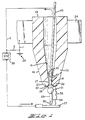
- FIG. 1 represents a capillary member 23, of known type, which is in fact of fine-grained alumina ceramic, containing approximately 99.8% of A1 2 0 3 , of beryllium oxide, of glass, of quartz, of ruby or polycrystalline sapphire, of precious stone of corundum group, such as ruby or sapphire or in other known materials.
- the member 23 is fixed to a heating support or to an ultrasonic transducer 24 of a welding machine.
- a wire 25, preferably made of gold, passes through the central duct of the member 23, which has a frustoconical part 15 and a capillary hole 17.
- This wire could also be made of another metal, such as aluminum, an aluminum alloy, palladium, copper, a copper alloy.
- the wire 25 and the support or transducer 24 are earthed 28 by conductors 1, 2, 3.
- a terminal of the generator 26 is earthed 28 by the conductor 3, while its other terminal is connected to a mobile electrode 27. At rest, the latter is separated from the member 23. When it comes to forming a ball 31, the electrode 27 is brought below the member 23, and then brought closer to the latter, but without touching the end 29 of the wire 25, which leaves the member 23. When this electrode has reached the desired position, the generator 26 is activated so as to produce a discharge 30 against the end 29 of the wire 25.
- the welding face 22 at the end of the member 23 normally comes into contact with the wire 25 and the metal of the output terminals of the envelope, possibly also with the metallized chip of the chip during welding, a thin metal film 32 is formed on the face 22.
- the wire 25 is fed through the member 23, it rubs against the frustoconical part 15 of its duct, which has the effect of producing a thin film 33 of the metal wire on this surface 15 of the member 23.
- the metallic films 32 and 33 offer a path of least resistance to the electric current of the discharge. When the latter occurs, the wire 25 and the ball 31 are strongly electrically charged.
- a spark or an electric arc 35 then occurs from the ball 31 and / or the wire 25 towards the film 32, as well as at 37, towards the film 33.
- a spark or an electric arc 36 can also occur directly between the electrode 27 and the film 32.
- the latter is heated and destroyed.
- the non-conductive material of the member 23 under this film is also destroyed by each spark, so that this results in a progressive erosion of the chamfer 18.
- the nature of this erosion is similar to that which is produced in machines. with EDM.
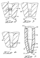
- Fig. 2 shows the damage 39 caused by sparking on the face 22 of a member 23 similar to that of FIG. 1 and made of non-conductive material.
- the main erosion normally occurs in the region of the chamfer 18 and in a part of the face 22, shown in broken lines.
- the chamfer 18 is hollowed out by erosion along the curvature of the ball 31, as is apparent from the eroded area 39.
- the spark or electric arc 37 (Fig. 1), which occurs where the wire 25 has rubbed against the surface 15, is less intense than that occurring against the face 22.
- the film 33 is much less important than that which forms on the face 22.
- the surface 15 is also more distant from the electrode 27 than the face 22.
- the spark 37 does not erode much the surface 15. However, it produces a burn and consequently a carbon deposit which tends to reduce the diameter of the conduit of the member 23 and ends up hampering the supply of the wire 25 through this conduit.
- this face becomes a good conductor. Direct sparking of the electrode 27 on this face becomes more important. The erosion then extends to this entire face 22 (shown in broken lines in FIG. 3), which flattens as shown at 42 in this figure.
- a capillary member made of an electrically conductive material such as tungsten carbide or titanium, such as member 43 of FIG. 4 erosion by sparking of this member occurs mainly in the hole 17, as shown in 44.
- the electric current seeks the path of least resistance and finds it in this case between the wire 25 and the walls of the hole 17 shown in broken lines in this figure.
- the resulting erosion therefore produces a widening of the outlet duct 17 of the member 23, which compromises the precision of the positioning of the welding points of the wire 25.
- Fig. 5 is a diametrical section of a capillary member according to the present invention. It has a body 45 which can be made of one or other of the materials mentioned above. Preferably, however, it will be made of a non-conductive material. This body is coated or plated with a conductive layer 46. In the case of a body 45 made of conductive material, a layer 46 will be chosen whose conductivity is significantly higher than that of the body 45. In general, the thickness of layer 46 does not need to exceed 0.0025 mm. This layer 46 must in particular be thin enough to adhere properly to the body 45, but still thick enough to constitute a good electrical conductor.
- the part of the layer 46 on the outer surface of the body 45 constitutes a path of low resistance to discharges coming from the electrode 27 through the part 16 of the layer 46, which covers the frustoconical part of the body 45 and which adjoins the face 22.
- the current of these discharges is thus conducted without damage to the ground 28 (Fig. 1).
- the capillary organ of FIG. 5 is intended to replace purely and simply that of FIG. 1.
- the path of the current coming from the electrode 27 is therefore composed of the layer 46 and of the support or of the ultrasonic transducer 24.
- the layer 46 consequently attracts the electric discharges far from the face 22 and protects it from the erosion.
- the layer 46 formed inside the body 45 has the same effect on the sparking shown at 37 in FIG. 1.
- the return to earth of this current from the wire 25 occurs through the part of the layer 46 lining the walls of the capillary duct of the member 45, 46, the part of this layer which covers the face 14 of the body. 45, its part on the external surface of the body 45 and finally the support or the ultrasonic transducer 24 of the welding machine.
- the carbon deposits on the walls of the capillary organ duct are thus practically eliminated.
- the layer 46 is applied to all the surfaces of the body 45. Elie would however not need to fill the walls of the hole 17 nor the welding face 22, comprising the chamfer 18 and the end 20 of the member nor the rounded external part 21. As it would be difficult to spare these surfaces during the formation of the layer 46, it is deposited everywhere. Following the first uses of this member, the electrical discharges will have eliminated the coating of the walls of the hole 17 and of the face 22 and exposed the body 45. The layer 46 covering the frusto-conical part 16 which adjoins the face 22 will then act as a lightning rod and will attract electrical discharges away from the face 22.
- a preferred embodiment of the capillary member according to the invention consists of a body made of fine-grained alumina ceramic, containing 99.8% of Al 2 0 3 and a conductive layer of titanium nitride applied to this body.
Landscapes
- Engineering & Computer Science (AREA)
- Mechanical Engineering (AREA)
- Wire Bonding (AREA)
- Details Of Resistors (AREA)
- Emergency Protection Circuit Devices (AREA)
Claims (5)
dadurch gekennzeichnet,
daß zumindest die Außenfläche des kegelstumpfartigen Abschnitts des Körpers sowie mindestens ein Teil der Innenfläche des Axialrohrs eine Überzugsschicht (46) aus einem leitenden Material aufweisen.
Priority Applications (1)
| Application Number | Priority Date | Filing Date | Title |
|---|---|---|---|
| AT84810001T ATE33354T1 (de) | 1983-01-03 | 1984-01-03 | Anordnung zum schutz gegen funkenspruehen eines kapillaren teiles das zum schweissen von draehten in einem halbleiterelement dient. |
Applications Claiming Priority (2)
| Application Number | Priority Date | Filing Date | Title |
|---|---|---|---|
| US455038 | 1983-01-03 | ||
| US06/455,038 US4513190A (en) | 1983-01-03 | 1983-01-03 | Protection of semiconductor wire bonding capillary from spark erosion |
Publications (3)
| Publication Number | Publication Date |
|---|---|
| EP0116010A2 EP0116010A2 (de) | 1984-08-15 |
| EP0116010A3 EP0116010A3 (en) | 1986-04-16 |
| EP0116010B1 true EP0116010B1 (de) | 1988-04-06 |
Family
ID=23807116
Family Applications (1)
| Application Number | Title | Priority Date | Filing Date |
|---|---|---|---|
| EP84810001A Expired EP0116010B1 (de) | 1983-01-03 | 1984-01-03 | Anordnung zum Schutz gegen Funkensprühen eines kapillaren Teiles das zum Schweissen von Drähten in einem Halbleiterelement dient |
Country Status (5)
| Country | Link |
|---|---|
| US (1) | US4513190A (de) |
| EP (1) | EP0116010B1 (de) |
| JP (1) | JPS59135738A (de) |
| AT (1) | ATE33354T1 (de) |
| DE (1) | DE3470290D1 (de) |
Families Citing this family (51)
| Publication number | Priority date | Publication date | Assignee | Title |
|---|---|---|---|---|
| US4674671A (en) * | 1985-11-04 | 1987-06-23 | Olin Corporation | Thermosonic palladium lead wire bonding |
| JPS62158335A (ja) * | 1985-12-28 | 1987-07-14 | Kyocera Corp | ワイヤボンディング用キャピラリ− |
| JPH02504487A (ja) * | 1987-08-17 | 1990-12-20 | シーメンス、アクチエンゲゼルシヤフト | 超音波溶接用工具装置 |
| US4909427A (en) * | 1989-05-17 | 1990-03-20 | Plaisted Alan H | Bonding wire ball formation |
| US4947024A (en) * | 1989-09-11 | 1990-08-07 | Alcotec Wire Co. | Welding apparatus coated with spatter-resistant and electrically conductive film |
| US5201453A (en) * | 1991-09-30 | 1993-04-13 | Texas Instruments Incorporated | Linear, direct-drive microelectronic bonding apparatus and method |
| US5772903A (en) * | 1996-09-27 | 1998-06-30 | Hirsch; Gregory | Tapered capillary optics |
| US5931368A (en) * | 1997-03-28 | 1999-08-03 | Kulicke And Soffa Investments, Inc | Long life bonding tool |
| US6045026A (en) | 1998-02-23 | 2000-04-04 | Micron Technology, Inc. | Utilize ultrasonic energy to reduce the initial contact forces in known-good-die or permanent contact systems |
| US6073827A (en) * | 1998-08-27 | 2000-06-13 | Kulicke & Soffa Investments, Inc. | Wire bonding capillary with a conical surface |
| US6309891B1 (en) * | 1998-09-09 | 2001-10-30 | Incyte Genomics, Inc. | Capillary printing systems |
| US6158647A (en) * | 1998-09-29 | 2000-12-12 | Micron Technology, Inc. | Concave face wire bond capillary |
| US6957783B1 (en) | 1999-01-26 | 2005-10-25 | Dl Technology Llc | Dispense tip with vented outlets |
| US6511301B1 (en) | 1999-11-08 | 2003-01-28 | Jeffrey Fugere | Fluid pump and cartridge |
| US7207498B1 (en) | 2000-01-26 | 2007-04-24 | Dl Technology, Llc | Fluid dispense tips |
| US6651864B2 (en) * | 1999-02-25 | 2003-11-25 | Steven Frederick Reiber | Dissipative ceramic bonding tool tip |
| US20060071050A1 (en) * | 1999-02-25 | 2006-04-06 | Reiber Steven F | Multi-head tab bonding tool |
| US7124927B2 (en) * | 1999-02-25 | 2006-10-24 | Reiber Steven F | Flip chip bonding tool and ball placement capillary |
| US20060261132A1 (en) * | 1999-02-25 | 2006-11-23 | Reiber Steven F | Low range bonding tool |
| US7032802B2 (en) * | 1999-02-25 | 2006-04-25 | Reiber Steven F | Bonding tool with resistance |
| US20080197172A1 (en) * | 1999-02-25 | 2008-08-21 | Reiber Steven F | Bonding Tool |
| US6354479B1 (en) * | 1999-02-25 | 2002-03-12 | Sjm Technologies | Dissipative ceramic bonding tip |
| US7389905B2 (en) * | 1999-02-25 | 2008-06-24 | Reiber Steven F | Flip chip bonding tool tip |
| US20070131661A1 (en) * | 1999-02-25 | 2007-06-14 | Reiber Steven F | Solder ball placement system |
| US6892959B1 (en) * | 2000-01-26 | 2005-05-17 | Dl Technology Llc | System and method for control of fluid dispense pump |
| US6981664B1 (en) | 2000-01-26 | 2006-01-03 | Dl Technology Llc | Fluid dispense tips |
| US6497356B2 (en) | 2000-04-28 | 2002-12-24 | Kulicke & Soffa Investments, Inc. | Controlled attenuation capillary with planar surface |
| US6321969B1 (en) * | 2000-04-28 | 2001-11-27 | Kulicke & Soffa Investments | Efficient energy transfer capillary |
| US6523733B2 (en) | 2000-04-28 | 2003-02-25 | Kulicke & Soffa Investments Inc. | Controlled attenuation capillary |
| AU2002240072A1 (en) | 2001-01-22 | 2002-07-30 | Gregory Hirsch | Pressed capillary optics |
| US6729527B2 (en) * | 2001-01-30 | 2004-05-04 | Kulicke & Soffa Investments, Inc. | Bonding tool with polymer coating |
| JP3621368B2 (ja) * | 2001-10-18 | 2005-02-16 | 株式会社新川 | ワイヤボンディング装置におけるボール形成装置 |
| CA2363409A1 (en) * | 2001-11-20 | 2003-05-20 | Microbonds, Inc. | A wire bonder for ball bonding insulated wire and method of using same |
| US6983867B1 (en) | 2002-04-29 | 2006-01-10 | Dl Technology Llc | Fluid dispense pump with drip prevention mechanism and method for controlling same |
| US7360675B2 (en) * | 2002-11-20 | 2008-04-22 | Microbonds, Inc. | Wire bonder for ball bonding insulated wire and method of using same |
| US7331482B1 (en) | 2003-03-28 | 2008-02-19 | Dl Technology, Llc | Dispense pump with heated pump housing and heated material reservoir |
| US7249702B2 (en) | 2003-12-04 | 2007-07-31 | Kulicke And Soffa Industries, Inc. | Multi-part capillary |
| US7322507B2 (en) * | 2005-01-17 | 2008-01-29 | Amkor Technology, Inc. | Transducer assembly, capillary and wire bonding method using the same |
| US20070085085A1 (en) * | 2005-08-08 | 2007-04-19 | Reiber Steven F | Dissipative pick and place tools for light wire and LED displays |
| US20080314963A1 (en) * | 2006-07-03 | 2008-12-25 | Kulicke And Soffa Industries, Inc. | Bonding Tool With Improved Finish |
| US8707559B1 (en) | 2007-02-20 | 2014-04-29 | Dl Technology, Llc | Material dispense tips and methods for manufacturing the same |
| JP4941268B2 (ja) * | 2007-12-17 | 2012-05-30 | 富士通株式会社 | ワイヤボンディング方法およびワイヤボンディング装置 |
| US7681456B2 (en) * | 2008-06-20 | 2010-03-23 | Rosemount Inc. | Field device including a capillary tube having a non-cylindrical lumen |
| US8864055B2 (en) | 2009-05-01 | 2014-10-21 | Dl Technology, Llc | Material dispense tips and methods for forming the same |
| CN102013405B (zh) * | 2009-09-04 | 2012-12-05 | 日月光封装测试(上海)有限公司 | 芯片打线接合装置的焊针加热构造及其方法 |
| US9725225B1 (en) | 2012-02-24 | 2017-08-08 | Dl Technology, Llc | Micro-volume dispense pump systems and methods |
| US9165904B1 (en) * | 2014-06-17 | 2015-10-20 | Freescale Semiconductor, Inc. | Insulated wire bonding with EFO before second bond |
| CN107052557B (zh) * | 2017-03-28 | 2019-09-24 | 潮州三环(集团)股份有限公司 | 一种具有涂层的焊接陶瓷劈刀 |
| US11746656B1 (en) | 2019-05-13 | 2023-09-05 | DL Technology, LLC. | Micro-volume dispense pump systems and methods |
| CN112077484B (zh) * | 2019-06-13 | 2022-08-16 | 湖南高精特电装备有限公司 | 一种钛合金锲形键合立针及其制备方法 |
| DE102022001130A1 (de) | 2022-03-25 | 2023-09-28 | Jonas Münz | Sonotrode sowie Vorrichtung und Verfahren zum Ultraschallschweißen von Stahl |
Family Cites Families (4)
| Publication number | Priority date | Publication date | Assignee | Title |
|---|---|---|---|---|
| US3358897A (en) * | 1964-03-31 | 1967-12-19 | Tempress Res Co | Electric lead wire bonding tools |
| JPS5549590B2 (de) * | 1972-06-10 | 1980-12-12 | ||
| US4315128A (en) * | 1978-04-07 | 1982-02-09 | Kulicke And Soffa Industries Inc. | Electrically heated bonding tool for the manufacture of semiconductor devices |
| DE3037735A1 (de) * | 1980-10-06 | 1982-05-13 | TS-Electronic Vertriebs-GmbH, 8000 München | Kontaktierverfahren und kontaktiermaschine zur durchfuehrung des verfahrens |
-
1983
- 1983-01-03 US US06/455,038 patent/US4513190A/en not_active Expired - Fee Related
- 1983-12-27 JP JP58244967A patent/JPS59135738A/ja active Pending
-
1984
- 1984-01-03 AT AT84810001T patent/ATE33354T1/de not_active IP Right Cessation
- 1984-01-03 EP EP84810001A patent/EP0116010B1/de not_active Expired
- 1984-01-03 DE DE8484810001T patent/DE3470290D1/de not_active Expired
Also Published As
| Publication number | Publication date |
|---|---|
| EP0116010A3 (en) | 1986-04-16 |
| DE3470290D1 (en) | 1988-05-11 |
| JPS59135738A (ja) | 1984-08-04 |
| US4513190A (en) | 1985-04-23 |
| EP0116010A2 (de) | 1984-08-15 |
| ATE33354T1 (de) | 1988-04-15 |
Similar Documents
| Publication | Publication Date | Title |
|---|---|---|
| EP0116010B1 (de) | Anordnung zum Schutz gegen Funkensprühen eines kapillaren Teiles das zum Schweissen von Drähten in einem Halbleiterelement dient | |
| EP0447295B1 (de) | Temperaturfühlerelement und Sonde mit einem solchen Element | |
| EP0318339B1 (de) | Funkenstrecken-Überspannungsableiter mit wenigstens einem Schmelzleiter | |
| JPS6126221B2 (de) | ||
| EP0524112B1 (de) | Spitze, insbesondere für Vakuumpipetten | |
| EP0003702B1 (de) | Schweissbrenner mit mechanischer und pneumatischer Reinigung | |
| US4909427A (en) | Bonding wire ball formation | |
| EP0002550B1 (de) | Verfahren zur Herstellung eines Kontakts auf der Oberfläche eines Halbleiterkörpers mittels Serigraphie und auf diese Weise hergestellte Anordnung | |
| EP0589748B1 (de) | Verfahren zur Vorbereitung der Montage eines Chips auf einem Substrat | |
| EP0262005B1 (de) | Herstellungsverfahren für eine bimetallische Mittelelektrode mit einem Platinstift für Zündkerze und Elektrode, hergestellt nach diesem Verfahren | |
| FR2799337A1 (fr) | Procede de realisation de connexions electriques sur la surface d'un boitier semi-conducteur a gouttes de connexion electrique | |
| EP0027061B1 (de) | Blitzableitervorrichtung, welche ein äusserliches Kurzschliessen erlaubt, und entsprechende Schutzeinheit | |
| FR2564827A1 (fr) | Procede pour braser une electrode metallique sur un element en ceramique en carbure de silicium electriquement conducteur et element en ceramique en carbure de silicium realise selon le procede | |
| FR2779368A1 (fr) | Torche de soudage tig permettant d'ameliorer l'amorcage de l'arc de soudage | |
| US3466158A (en) | Compound precious metal article having layer containing iridium or ruthenium | |
| EP0219361B1 (de) | Verkleinerte Vorrichtung zur Verbindung von elektrisch leitenden Elementen für sehr hohe Stromstärken | |
| FR2758661A1 (fr) | Dispositif de raccordement mecanique et de connexion electrique | |
| CH620618A5 (de) | ||
| EP0554195A1 (de) | Selbsttätig geschütztes Halbleiterschutzelement | |
| US4987341A (en) | Flash lamp with metal coating on an outer end of an electrode thereof | |
| FR2539658A1 (fr) | Tube de guidage d'un fil de metal d'apport pour une installation de soudage par arc electrique | |
| FR2572852A1 (fr) | Dispositif semi-conducteur en particulier thyristor comportant une electrode d'acces a l'electrode de commande | |
| WO1998054937A1 (fr) | Adaptateur pour composants electroniques | |
| JP3973319B2 (ja) | ワイヤボンダの電気トーチ | |
| FR2848026A1 (fr) | Dispositif de protection d'un circuit electronique contre des decharges electrostatiques |
Legal Events
| Date | Code | Title | Description |
|---|---|---|---|
| PUAI | Public reference made under article 153(3) epc to a published international application that has entered the european phase |
Free format text: ORIGINAL CODE: 0009012 |
|
| AK | Designated contracting states |
Designated state(s): AT CH DE FR GB IT LI |
|
| PUAL | Search report despatched |
Free format text: ORIGINAL CODE: 0009013 |
|
| AK | Designated contracting states |
Kind code of ref document: A3 Designated state(s): AT CH DE FR GB IT LI |
|
| 17P | Request for examination filed |
Effective date: 19860509 |
|
| 17Q | First examination report despatched |
Effective date: 19870218 |
|
| GRAA | (expected) grant |
Free format text: ORIGINAL CODE: 0009210 |
|
| ITF | It: translation for a ep patent filed | ||
| AK | Designated contracting states |
Kind code of ref document: B1 Designated state(s): AT CH DE FR GB IT LI |
|
| PG25 | Lapsed in a contracting state [announced via postgrant information from national office to epo] |
Ref country code: AT Effective date: 19880406 |
|
| REF | Corresponds to: |
Ref document number: 33354 Country of ref document: AT Date of ref document: 19880415 Kind code of ref document: T |
|
| GBT | Gb: translation of ep patent filed (gb section 77(6)(a)/1977) | ||
| REF | Corresponds to: |
Ref document number: 3470290 Country of ref document: DE Date of ref document: 19880511 |
|
| PGFP | Annual fee paid to national office [announced via postgrant information from national office to epo] |
Ref country code: FR Payment date: 19881223 Year of fee payment: 6 |
|
| PG25 | Lapsed in a contracting state [announced via postgrant information from national office to epo] |
Ref country code: LI Effective date: 19890131 Ref country code: CH Effective date: 19890131 |
|
| PLBE | No opposition filed within time limit |
Free format text: ORIGINAL CODE: 0009261 |
|
| STAA | Information on the status of an ep patent application or granted ep patent |
Free format text: STATUS: NO OPPOSITION FILED WITHIN TIME LIMIT |
|
| 26N | No opposition filed | ||
| REG | Reference to a national code |
Ref country code: CH Ref legal event code: PL |
|
| PGFP | Annual fee paid to national office [announced via postgrant information from national office to epo] |
Ref country code: GB Payment date: 19900131 Year of fee payment: 7 |
|
| PGFP | Annual fee paid to national office [announced via postgrant information from national office to epo] |
Ref country code: DE Payment date: 19900202 Year of fee payment: 7 |
|
| PG25 | Lapsed in a contracting state [announced via postgrant information from national office to epo] |
Ref country code: FR Effective date: 19900928 |
|
| REG | Reference to a national code |
Ref country code: FR Ref legal event code: ST |
|
| PG25 | Lapsed in a contracting state [announced via postgrant information from national office to epo] |
Ref country code: GB Effective date: 19910103 |
|
| GBPC | Gb: european patent ceased through non-payment of renewal fee | ||
| PG25 | Lapsed in a contracting state [announced via postgrant information from national office to epo] |
Ref country code: DE Effective date: 19911001 |