EP0116304B1 - Dispositif semi-conducteur optique composé - Google Patents
Dispositif semi-conducteur optique composé Download PDFInfo
- Publication number
- EP0116304B1 EP0116304B1 EP84100337A EP84100337A EP0116304B1 EP 0116304 B1 EP0116304 B1 EP 0116304B1 EP 84100337 A EP84100337 A EP 84100337A EP 84100337 A EP84100337 A EP 84100337A EP 0116304 B1 EP0116304 B1 EP 0116304B1
- Authority
- EP
- European Patent Office
- Prior art keywords
- region
- electrode
- semiconductor device
- composite optical
- optical semiconductor
- Prior art date
- Legal status (The legal status is an assumption and is not a legal conclusion. Google has not performed a legal analysis and makes no representation as to the accuracy of the status listed.)
- Expired
Links
- 239000004065 semiconductor Substances 0.000 title claims description 25
- 239000002131 composite material Substances 0.000 title claims description 18
- 230000003287 optical effect Effects 0.000 title claims description 18
- 239000000758 substrate Substances 0.000 claims description 8
- 239000013307 optical fiber Substances 0.000 claims description 7
- 229910001218 Gallium arsenide Inorganic materials 0.000 description 19
- 239000012535 impurity Substances 0.000 description 13
- 238000012544 monitoring process Methods 0.000 description 6
- 230000001419 dependent effect Effects 0.000 description 3
- 239000002184 metal Substances 0.000 description 2
- 230000005540 biological transmission Effects 0.000 description 1
- 239000012141 concentrate Substances 0.000 description 1
- 238000010276 construction Methods 0.000 description 1
- 230000000994 depressogenic effect Effects 0.000 description 1
- 238000004519 manufacturing process Methods 0.000 description 1
- 239000000463 material Substances 0.000 description 1
Images


Classifications
-
- H—ELECTRICITY
- H10—SEMICONDUCTOR DEVICES; ELECTRIC SOLID-STATE DEVICES NOT OTHERWISE PROVIDED FOR
- H10F—INORGANIC SEMICONDUCTOR DEVICES SENSITIVE TO INFRARED RADIATION, LIGHT, ELECTROMAGNETIC RADIATION OF SHORTER WAVELENGTH OR CORPUSCULAR RADIATION
- H10F55/00—Radiation-sensitive semiconductor devices covered by groups H10F10/00, H10F19/00 or H10F30/00 being structurally associated with electric light sources and electrically or optically coupled thereto
- H10F55/18—Radiation-sensitive semiconductor devices covered by groups H10F10/00, H10F19/00 or H10F30/00 being structurally associated with electric light sources and electrically or optically coupled thereto wherein the radiation-sensitive semiconductor devices and the electric light source share a common body having dual-functionality of light emission and light detection
Definitions
- This invention relates to a composite optical semiconductor device including a light emitting element and a light detecting element in one body.
- a light emitting diode has such an output characteristic that the fluctuation dependent on the temperature is smaller than that of a semiconductor laser device.
- the output characteristic is more linear.
- a LED is a source of light easy to deal with except for the problems of power level and response speed. But, if the LED is actually used in ananalog transmission system, nevertheless the fluctuation of its output characteristic must be compensated.
- a wideband opto-electric negative feedback (NFB) loop is widely used for compensating both the fluctuation dependent or the temperature and the nonlinearity at the same time as explained in the paper MJ2 of I00C '81, San Francisco in U.S.A. (1981).
- nonlinear distortion of the LED is compensated by a negative feedback of a part of a light output to a driver circuit of the LED after detecting the part of the light output of the LED. Then it is desirable to construct in a body a light emitting element and a light detecting element in order to compensate the nonlinear distortion.
- a prior art composite optical semiconductor device which includes in a body a LED and a photo detector (PD), is shown in Figure 1; this device corresponds to that of the preamble of claim 1.
- the LED is constructed as follows.
- a P-type GaAlAs layer 3 is formed on a N-type GaAs current confinement layer 2 which is formed on a P-type GaAs substrate 1.
- the P-type layer 3 penetrates the current confinement layer 2 in the center area thereof.
- a N-type GaAlAs layer 5 is formed on a N-type GaAs active layer 4 which is formed on the P-type layer 3.
- the LED emits a light in the active layer 4 by applying a voltage between a first electrode 6 and a second electrode 7.
- a PD comprises the N-type GaAlAs layer 5, a GaAlAs intrinsic layer 8 and a P-type GaAs layer 9.
- the PD has a P-I-N construction.
- the PD is operated by applying a voltage between a third electrode 10, formed on the P-type GaAs layer 9, and said second electrode 7. Namely, the N-type GaAlAs layer 5 and the electrode 7 are used in common in the LED and the PD.
- a light emitted from the active layer 4 is detected by the PD and is transmitted to the outside through a light transmitting portion 11 which is formed in the center of the device.
- the light output from the transmitting portion 11 enters into an optical fibre 12.
- the electrical output of the PD supplies an outside electrical circuit which is part of a wideband opto-electric NFB loop in order to control a driver circuit of the LED.
- the PD In the wideband opto-electric NFB loop, it is necessary to get an exact monitoring current dependent on the light of the LED which passes the PD.
- the PD detects this part of the light output of the LED. But it is difficult to get a correct monitoring current in the prior art device. Because in the prior art device, the electrode 7 is used in common for the LED and for the PD and is constructed outside of the detecting portion of the PD, the current path of the LED is close to that of the PD, and both paths partly overlap each other. Therefore, a leak current flows from the LED to the PD, and the PD may detect a wrong monitoring current of the light of the LED.
- DE-A-3 106 798 discloses a circuit structure including an integrated light emitting diode and a FET in which a middle portion of a layer of the structure constitutes the drain of the FET as well as a portion of the diode. Using a common electrode there result overlapping current paths for both the diode and the drain zone of the FET.
- Figure 1 shows a diagrammatic view, partly in section, of a prior art composite optical semiconductor device
- Figure 2 shows a diagrammatic view, partly in section, of a preferred embodiment of this invention
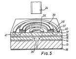
- FIGS 3 to 5 show further embodiments of this invention.
- a P-type GaAs substrate 13 is used as a substrate of a LED.
- the substrate 13 has impurities of a concentration of 1 x 1018 cm ⁇ 3 and a thickness of 100 to 200 ⁇ m.
- a current confinement layer 14 is formed on the substrate 13 and is provided with a window in order to concentrate the current of the LED and to get a high light emitting efficiency.
- the confinement layer 14 is made of N-type GaAs having impurities of a concentration of 1 x 1018 cm ⁇ 3 and a thickness of 4 to 5 ⁇ m.
- a first component layer 15 is formed within the area of the window of the confinement layer 14 on the substrate 13 and on the current confinement layer 14.
- the first component layer 15 is made of P-type Ga 1-x Al x As having impurities of a concentration of 1 x 1018 cm ⁇ 3 and the thickness of 4 to 5 ⁇ m, wherein x is 0.3 to 0.4.
- An active layer 16 is formed on the first component layer 15.
- the active layer 16 is made of N-type GaAs having impurities of a concentration of 1 x 1018 cm ⁇ 3 and a thickness of 1 ⁇ m.
- a second component layer 17 is formed on the active layer 16.
- the second component layer 17 is made of N-type Ga 1-x Al x As having impurities of a concentration of 1 x 1018 cm ⁇ 3 and a thickness of 5 ⁇ m, wherein x is 0.3 to 0.4.
- light is emitted in the active layer 16 by applying a voltage between a first electrode 18 and a second electrode 19.
- the electrodes 18 and 19 are made of metal.
- a GaAlAs layer 20 is formed circularly on a part of said N-type layer 17, the latter being used as a component of the PD and also as the second component layer 17 of the LED.
- the GaAlAs layer 20 has impurities of low concentration as it is used for an intrinsic layer and has a thickness of about 10 ⁇ m.
- a P-type GaAs layer 21 is formed on the GaAlAs layer 20.
- the GaAs layer 21 has a thickness of 3 ⁇ m and impurities of a concentration of 1 x 1018 cm ⁇ 3.
- a P-type GaAs layer 22 is formed in the P-type GaAs layer 21 in order to have a good ohmic contact with a third electrode 23 made of metal.
- the P-type GaAs layer 22 has impurities more than that of the P-type GaAs layer 21.
- the PD can be operated by applying a voltage between the third electrode 23 and a second electrode 19 which is also the second electrode 19 of the LED.
- the electrode 19 has a width of about 30 ⁇ m and is formed circularly inside of and spaced from the detecting portion i.e. the intrinsic layer 20 of the PD.
- the detecting portion of the PD has a width of about 50 ⁇ m to 70 ⁇ m.
- part of the light output from the active layer 16 of the LED is detected by the PD and a part of the light output enters an optical fibre 24 through a light transmitting portion 25 which is inside and outside of the nontransparent electrode 19.
- the electrical output of the PD is led to an outside electrical circuit, part thereof being a wideband opto-electric NFB loop.
- the electrode 19, which is commonly used for the LED and for the PD is formed inside of the photo detecting portion, and has generally earth voltage. Therefore the current paths of the LED and the PD are separated from each other sufficiently and do not overlap each other, and a leak current from the LED to the PD is prevented.
- the PD detects the correct monitoring current of the LED.
- the electrode 19 may be formed triangularly, squarely, polygonaly or elliptically instead of circularly. But the efficiency of the light output must be considered because the electrode is generally made of nontransparent material.
- FIG. 3 A LED is formed similarly to the first embodiment according to Fig. 2. But in this case the PD has a plurality of detecting portions. Namely, the detecting portion of the PD according to the first embodiment is divided into plural parts arranged concentrically on the second component layer 17.
- the PD includes three concentric GaAlAs layers 26, which have impurities of low concentration, P-type GaAs layers 27, P-type GaAs layers 28 for good ohmic contact, and third electrodes 29.
- the plural detecting portions are formed with concentric circles outside of the second electrode 19 which is also one of the electrodes of the LED.
- the third electrodes 29 of the PD are short circuited by one another and connected to earth voltage.
- the light output from the LED enters also an optical fibre 24.
- the non-linear characteristic of the light of the center is generally different from that of the light of the periphery.
- the optical fibre 24 receives the light from the entire surface of the device. At the same time, a part of the light is detected by the photo detecting portions 26 and the PD monitors the light of the LED more correctly. As the photo detecting portions 26 are divided into plural parts, compared with the device according to Fig. 2, sufficient light from the LED enters the optical fibre 24.
- FIG. 4 Another embodiment is shown in Figure 4.
- a LED is formed similar to the first embodiment according to Fig. 2.
- a PD is formed on a second component layer 17 of the LED.
- a GaAlAs layer 30, which has impurities of a low concentration, is formed on part of the N-Type layer 17 and a P-type GaAs layer 31 is formed thereon.
- the PD has also a P-I-N structure and can be operated by a voltage between a third electrode 32 and, a second electrode 33.
- the second electrode is connected to the N-type layer 17 through a N-type region 34, the concentration of impurities thereof being higher than the concentration of impurities of the N-type layer 17.
- the second electrode 33 of the PD is also one of the electrodes of the LED.
- the light output from the LED enters an optical fibre 24 similarly as in the embodiment according to Fig. 2 and is detected and monitored by the PD and the outside circuit at the same time. It is easy to align a mask in a manufacturing step producing this embodiment. Namely, the electrodes 19 of the first and second embodiments must be formed on the depressed portions after having formed the PD, but the electrode 33 of this embodiment can be formed easily and precisely on the P-type region 34.
- a LED of this embodiment is formed similarly to the first embodiment according to Fig. 2.
- the LED emits a light from an active layer 16 by applying a voltage between a first electrode 18 and a second electrode 35.
- a current path 36 of the LED is confined to the center by a current confinement layer 14.
- a PD comprises a GaAs intrinsic layer 37 and a P-type GaAs layer 38 which are formed on a N-type layer 17. This layer is the second component layer 17 of the LED.
- the PD can be operated by applying a voltage between a third electrode 39 and a fourth electrode 40.
- the fourth electrode 40 is formed circularly outside of and spaced from the photo detecting portion i.e. the intrinsic layer 37.
- a current path 41 of the PD is formed between the third and fourth electrodes 39 and 40. This current path is formed apart from the current path 36 of the LED between the first and second electrodes 18 and 35. Namely, the current path 41 of the PD is independent of the current path 36 of the LED. Therefore, a leak current from the LED to the PD is reduced to a neglectable amount, and the PD detects the correct monitoring current. It is effective to form the current paths of the LED and the PD independently, and then the leak current from the LED to the PD can be reduced to less than 1 % of the detecting current of the PD.
Landscapes
- Semiconductor Lasers (AREA)
- Led Devices (AREA)
Claims (13)
- Dispositif semiconducteur optique composite comprenant un élément gui émet de la lumière et un élément qui détecte la lumière, ce dispositif comportant :une première région semiconductrice (13/15) ayant un premier type de conductivité (type P) formée dans un substrat semiconducteur, une seconde région semiconductrice (17) ayant un second type de conductivité (type N) et formant avec la première région l'élément qui émet de la lumière, cet élément comprenant une jonction PN ;une couche de confinement du courant (14) présentant une ouverture formée dans la première ou dans la seconde région (13/15 ou 17), une première électrode (18) connectée à la première région (13/15) ;une seconde électrode (19, 33 ; 35) connectée à la seconde région (17) ;une partie qui transmet de la lumière (25), cette partie transmettant la lumière émise du fait de l'application d'une tension entre les première et seconde électrodes ;une troisième région semiconductrice (20/21/22 ; 26/27/28 ; 30/31 ; 37/38) formant avec la seconde région (17) l'élément qui détecte la lumière, cet élément détectant une partie de la lumière émise ;une troisième électrode (23 ; 29 ; 32 ; 39) connectée à la troisième région ; etune quatrième électrode (19, 33 ; 40) connectée à la seconde région ;électrode (19, 33, 35) et en ce que la troisième région (20/21/22 ; 26/27/28 ; 37/38) est formée autour de la seconde électrode (19, 33 ; 35), de sorte que la voie de courant principal entre les troisième et quatrième électrodes (23 ; 29 ; 32 ; 39, 19, 33 ; 40) soit formée de manière sensiblement indépendante d'une voie de courant principale située entre les première et seconde électrodes (18, 19, 33 ; 35).
caractérisé en ce que l'élément qui détecte la lumière est formé autour de l'élément qui émet de la lumière, en ce que la partie qui transmet la lumière (25) est formée au niveau de la partie centrale de la seconde - Dispositif semiconducteur optique composite selon la revendication l, dans lequel la seconde électrode (19 ; 33) est identique à la quatrième électrode.
- Dispositif semiconducteur optique composite selon la revendication 2, dans lequel la troisième région (20/21/22 ; 26/27/28 ; 30/31) et la troisième électrode (23 ; 29 ; 32) ont une forme annulaire et dans lequel la seconde électrode (19 ; 33) est disposée à l'intérieur des troisième région et troisième électrode, dans la surface de la partie (25) qui transmet la lumière.
- Dispositif semiconducteur optique composite selon la revendication 3, dans lequel la troisième région et la troisième électrode ont une forme de bague circulaire.
- Dispositif semiconducteur optique composite selon la revendication 3 ou 4, dans lequel la troisième région (26/27/28) comprend une pluralité de bagues concentriques espacées les unes des autres et disposées autour de la seconde électrode (19) et dans lequel les troisièmes électrodes (29) sont connectées à chacune des troisièmes régions.
- Dispositif semiconducteur optique composite selon l'une quelconque des revendications 1 à 5, dans lequel la troisième région a le premier type de conductivité (type P).
- Dispositif semiconducteur optique composite selon l'une quelconque des revendications 1 à 6, dans lequel la troisième région comprend une couche intrinsèque (20 ; 26 ; 30 ; 37) adjacente à la seconde région.
- Dispositif semiconducteur optique composite selon la revendication 7, dans lequel une fibre optique (24) est disposée au-dessus de la zone déterminée par l'ouverture ménagée dans la couche de confinement du courant (14).
- Dispositif semiconducteur optique composite selon la revendication 1, comprenant en outre une quatrième région semiconductrice (34) formée de manière adjacente à la troisième région (30/31), cette quatrième région ayant le même type de conductivité (type N) que la seconde région (17), et dans lequel la seconde électrode (33) est formée sur la quatrième région (34).
- Dispositif semiconducteur optique composite selon la revendication 1, dans lequel la première région est formée dans la seconde région.
- Dispositif semiconducteur optique composite selon la revendication 1, dans lequel la troisième région est formée sur la seconde région.
- Dispositif semiconducteur optique composite selon l'une quelconque des revendications 1 à 11, comprenant en outre une couche active (16) formée entre la première région (13/15) et la seconde région (17).
- Dispositif semiconducteur optique composite selon l'une quelconque des revendications 1 à 12, comprenant en outre un circuit de contrôle pour une boucle à contre-réaction opto-électrique à large bande formée dans ou sur le substrat semiconducteur.
Applications Claiming Priority (4)
| Application Number | Priority Date | Filing Date | Title |
|---|---|---|---|
| JP58003359A JPS59129467A (ja) | 1983-01-14 | 1983-01-14 | 複合光半導体素子 |
| JP3359/83 | 1983-01-14 | ||
| JP73802/83 | 1983-04-28 | ||
| JP58073802A JPS59200475A (ja) | 1983-04-28 | 1983-04-28 | 複合光半導体素子 |
Publications (3)
| Publication Number | Publication Date |
|---|---|
| EP0116304A2 EP0116304A2 (fr) | 1984-08-22 |
| EP0116304A3 EP0116304A3 (en) | 1986-10-15 |
| EP0116304B1 true EP0116304B1 (fr) | 1991-04-17 |
Family
ID=26336919
Family Applications (1)
| Application Number | Title | Priority Date | Filing Date |
|---|---|---|---|
| EP84100337A Expired EP0116304B1 (fr) | 1983-01-14 | 1984-01-13 | Dispositif semi-conducteur optique composé |
Country Status (2)
| Country | Link |
|---|---|
| EP (1) | EP0116304B1 (fr) |
| DE (1) | DE3484443D1 (fr) |
Families Citing this family (2)
| Publication number | Priority date | Publication date | Assignee | Title |
|---|---|---|---|---|
| GB2312346B (en) * | 1996-04-20 | 2000-07-12 | Northern Telecom Ltd | Marshalling in optical tdma systems |
| TWI276230B (en) * | 2001-12-04 | 2007-03-11 | Epitech Corp Ltd | Structure and manufacturing method of light emitting diode |
Family Cites Families (4)
| Publication number | Priority date | Publication date | Assignee | Title |
|---|---|---|---|---|
| US4136928A (en) * | 1977-05-06 | 1979-01-30 | Bell Telephone Laboratories, Incorporated | Optical integrated circuit including junction laser with oblique mirror |
| US4275404A (en) * | 1979-10-05 | 1981-06-23 | Bell Telephone Laboratories, Incorporated | Monolithic opto-isolator |
| GB2094060B (en) * | 1981-02-23 | 1985-04-17 | Omron Tateisi Electronics Co | Light emitting and receiving device |
| DE3106798A1 (de) * | 1981-02-24 | 1982-09-09 | Licentia Patent-Verwaltungs-Gmbh, 6000 Frankfurt | Halbleiteranordnung |
-
1984
- 1984-01-13 DE DE8484100337T patent/DE3484443D1/de not_active Expired - Lifetime
- 1984-01-13 EP EP84100337A patent/EP0116304B1/fr not_active Expired
Also Published As
| Publication number | Publication date |
|---|---|
| EP0116304A3 (en) | 1986-10-15 |
| DE3484443D1 (de) | 1991-05-23 |
| EP0116304A2 (fr) | 1984-08-22 |
Similar Documents
| Publication | Publication Date | Title |
|---|---|---|
| US5557117A (en) | Heterojunction bipolar transistor and integrated circuit device using the same | |
| US4485391A (en) | Light emitting and receiving transistor for operation in alternate _sequence in an optical-fiber telecommunications systems | |
| US4605943A (en) | Composite optical semiconductor device | |
| US5892787A (en) | N-drive, p-common light-emitting devices fabricated on an n-type substrate and method of making same | |
| CA1150808A (fr) | Laser a semiconducteurs | |
| US5887013A (en) | Light emitting apparatus | |
| US4213138A (en) | Demultiplexing photodetector | |
| US5010381A (en) | Semiconductor light receiving element | |
| US4614958A (en) | Light emitting and receiving device | |
| JP2597975B2 (ja) | 半導体発光素子及びその製造方法 | |
| US20130207160A1 (en) | Semiconductor light detecting element | |
| EP0532025A1 (fr) | Dispositif semi-conducteur optique ayant un laser à semi-conducteur et un photodétecteur | |
| US4779281A (en) | Light emitting chip and optical communication apparatus using the same | |
| US5748661A (en) | Integrated lateral detector and laser device and method of fabrication | |
| US4740823A (en) | Photo-detectors | |
| US4323911A (en) | Demultiplexing photodetectors | |
| EP0501246B1 (fr) | Dispositif interrupteur optoélectronique | |
| US5061977A (en) | Semiconductor photodetector device | |
| JP2006216846A (ja) | 面発光型装置及びその製造方法 | |
| EP0116304A2 (fr) | Dispositif semi-conducteur optique composé | |
| CA2051453C (fr) | Circuit opto-electronique integre a emetteur de lumiere a grande longueur d'onde | |
| EP0616374B1 (fr) | Dispositif semi-conducteur détecteur de lumière | |
| EP0260439B1 (fr) | Dispositif à semi-conducteur d'émission de lumière | |
| JP2000004047A (ja) | 半導体発光装置及びその製造方法 | |
| US5684307A (en) | Semiconductor photodiode having the electrodes formed on the same surface |
Legal Events
| Date | Code | Title | Description |
|---|---|---|---|
| PUAI | Public reference made under article 153(3) epc to a published international application that has entered the european phase |
Free format text: ORIGINAL CODE: 0009012 |
|
| 17P | Request for examination filed |
Effective date: 19840113 |
|
| AK | Designated contracting states |
Designated state(s): DE FR GB |
|
| RAP1 | Party data changed (applicant data changed or rights of an application transferred) |
Owner name: KABUSHIKI KAISHA TOSHIBA |
|
| PUAL | Search report despatched |
Free format text: ORIGINAL CODE: 0009013 |
|
| AK | Designated contracting states |
Kind code of ref document: A3 Designated state(s): DE FR GB |
|
| 17Q | First examination report despatched |
Effective date: 19890303 |
|
| GRAA | (expected) grant |
Free format text: ORIGINAL CODE: 0009210 |
|
| AK | Designated contracting states |
Kind code of ref document: B1 Designated state(s): DE FR GB |
|
| REF | Corresponds to: |
Ref document number: 3484443 Country of ref document: DE Date of ref document: 19910523 |
|
| ET | Fr: translation filed | ||
| PLBE | No opposition filed within time limit |
Free format text: ORIGINAL CODE: 0009261 |
|
| STAA | Information on the status of an ep patent application or granted ep patent |
Free format text: STATUS: NO OPPOSITION FILED WITHIN TIME LIMIT |
|
| 26N | No opposition filed | ||
| PGFP | Annual fee paid to national office [announced via postgrant information from national office to epo] |
Ref country code: GB Payment date: 19980105 Year of fee payment: 15 |
|
| PGFP | Annual fee paid to national office [announced via postgrant information from national office to epo] |
Ref country code: FR Payment date: 19980109 Year of fee payment: 15 |
|
| PGFP | Annual fee paid to national office [announced via postgrant information from national office to epo] |
Ref country code: DE Payment date: 19980116 Year of fee payment: 15 |
|
| PG25 | Lapsed in a contracting state [announced via postgrant information from national office to epo] |
Ref country code: GB Free format text: LAPSE BECAUSE OF NON-PAYMENT OF DUE FEES Effective date: 19990113 |
|
| GBPC | Gb: european patent ceased through non-payment of renewal fee |
Effective date: 19990113 |
|
| PG25 | Lapsed in a contracting state [announced via postgrant information from national office to epo] |
Ref country code: FR Free format text: LAPSE BECAUSE OF NON-PAYMENT OF DUE FEES Effective date: 19990930 |
|
| PG25 | Lapsed in a contracting state [announced via postgrant information from national office to epo] |
Ref country code: DE Free format text: LAPSE BECAUSE OF NON-PAYMENT OF DUE FEES Effective date: 19991103 |
|
| REG | Reference to a national code |
Ref country code: FR Ref legal event code: ST |