EP0501246B1 - Dispositif interrupteur optoélectronique - Google Patents
Dispositif interrupteur optoélectronique Download PDFInfo
- Publication number
- EP0501246B1 EP0501246B1 EP92102438A EP92102438A EP0501246B1 EP 0501246 B1 EP0501246 B1 EP 0501246B1 EP 92102438 A EP92102438 A EP 92102438A EP 92102438 A EP92102438 A EP 92102438A EP 0501246 B1 EP0501246 B1 EP 0501246B1
- Authority
- EP
- European Patent Office
- Prior art keywords
- semiconductor layer
- layer
- type
- semiconductor
- switch device
- Prior art date
- Legal status (The legal status is an assumption and is not a legal conclusion. Google has not performed a legal analysis and makes no representation as to the accuracy of the status listed.)
- Expired - Lifetime
Links
- 230000005693 optoelectronics Effects 0.000 title claims description 31
- 239000004065 semiconductor Substances 0.000 claims description 92
- 239000000758 substrate Substances 0.000 claims description 25
- 238000000034 method Methods 0.000 claims description 7
- 238000004519 manufacturing process Methods 0.000 claims description 3
- 238000005468 ion implantation Methods 0.000 claims 1
- 229910000980 Aluminium gallium arsenide Inorganic materials 0.000 description 70
- 229910001218 Gallium arsenide Inorganic materials 0.000 description 59
- 238000009792 diffusion process Methods 0.000 description 17
- 239000000203 mixture Substances 0.000 description 12
- VYPSYNLAJGMNEJ-UHFFFAOYSA-N Silicium dioxide Chemical compound O=[Si]=O VYPSYNLAJGMNEJ-UHFFFAOYSA-N 0.000 description 8
- 230000009471 action Effects 0.000 description 5
- 238000003475 lamination Methods 0.000 description 5
- 239000000969 carrier Substances 0.000 description 4
- 229910052681 coesite Inorganic materials 0.000 description 4
- 229910052906 cristobalite Inorganic materials 0.000 description 4
- 238000005516 engineering process Methods 0.000 description 4
- 238000002347 injection Methods 0.000 description 4
- 239000007924 injection Substances 0.000 description 4
- 239000000377 silicon dioxide Substances 0.000 description 4
- 229910052682 stishovite Inorganic materials 0.000 description 4
- 229910052905 tridymite Inorganic materials 0.000 description 4
- 239000011701 zinc Substances 0.000 description 4
- 229910000530 Gallium indium arsenide Inorganic materials 0.000 description 3
- 125000004429 atom Chemical group 0.000 description 3
- 230000004927 fusion Effects 0.000 description 3
- 230000006872 improvement Effects 0.000 description 3
- 229920002120 photoresistant polymer Polymers 0.000 description 3
- 229910000990 Ni alloy Inorganic materials 0.000 description 2
- 229910045601 alloy Inorganic materials 0.000 description 2
- 239000000956 alloy Substances 0.000 description 2
- 238000006243 chemical reaction Methods 0.000 description 2
- 230000000694 effects Effects 0.000 description 2
- 238000005530 etching Methods 0.000 description 2
- 238000004020 luminiscence type Methods 0.000 description 2
- 238000001451 molecular beam epitaxy Methods 0.000 description 2
- 230000003071 parasitic effect Effects 0.000 description 2
- 238000001771 vacuum deposition Methods 0.000 description 2
- 230000001133 acceleration Effects 0.000 description 1
- 230000005540 biological transmission Effects 0.000 description 1
- 230000006870 function Effects 0.000 description 1
- 125000005842 heteroatom Chemical group 0.000 description 1
- 238000001459 lithography Methods 0.000 description 1
- 230000033001 locomotion Effects 0.000 description 1
- 230000003287 optical effect Effects 0.000 description 1
- 239000013307 optical fiber Substances 0.000 description 1
- 230000009467 reduction Effects 0.000 description 1
- 230000004044 response Effects 0.000 description 1
- JBQYATWDVHIOAR-UHFFFAOYSA-N tellanylidenegermanium Chemical group [Te]=[Ge] JBQYATWDVHIOAR-UHFFFAOYSA-N 0.000 description 1
Images


Classifications
-
- H—ELECTRICITY
- H01—ELECTRIC ELEMENTS
- H01S—DEVICES USING THE PROCESS OF LIGHT AMPLIFICATION BY STIMULATED EMISSION OF RADIATION [LASER] TO AMPLIFY OR GENERATE LIGHT; DEVICES USING STIMULATED EMISSION OF ELECTROMAGNETIC RADIATION IN WAVE RANGES OTHER THAN OPTICAL
- H01S5/00—Semiconductor lasers
- H01S5/10—Construction or shape of the optical resonator, e.g. extended or external cavity, coupled cavities, bent-guide, varying width, thickness or composition of the active region
- H01S5/18—Surface-emitting [SE] lasers, e.g. having both horizontal and vertical cavities
- H01S5/183—Surface-emitting [SE] lasers, e.g. having both horizontal and vertical cavities having only vertical cavities, e.g. vertical cavity surface-emitting lasers [VCSEL]
- H01S5/18305—Surface-emitting [SE] lasers, e.g. having both horizontal and vertical cavities having only vertical cavities, e.g. vertical cavity surface-emitting lasers [VCSEL] with emission through the substrate, i.e. bottom emission
-
- H—ELECTRICITY
- H10—SEMICONDUCTOR DEVICES; ELECTRIC SOLID-STATE DEVICES NOT OTHERWISE PROVIDED FOR
- H10H—INORGANIC LIGHT-EMITTING SEMICONDUCTOR DEVICES HAVING POTENTIAL BARRIERS
- H10H20/00—Individual inorganic light-emitting semiconductor devices having potential barriers, e.g. light-emitting diodes [LED]
- H10H20/01—Manufacture or treatment
- H10H20/011—Manufacture or treatment of bodies, e.g. forming semiconductor layers
- H10H20/013—Manufacture or treatment of bodies, e.g. forming semiconductor layers having light-emitting regions comprising only Group III-V materials
-
- H—ELECTRICITY
- H10—SEMICONDUCTOR DEVICES; ELECTRIC SOLID-STATE DEVICES NOT OTHERWISE PROVIDED FOR
- H10H—INORGANIC LIGHT-EMITTING SEMICONDUCTOR DEVICES HAVING POTENTIAL BARRIERS
- H10H20/00—Individual inorganic light-emitting semiconductor devices having potential barriers, e.g. light-emitting diodes [LED]
- H10H20/80—Constructional details
- H10H20/81—Bodies
- H10H20/813—Bodies having a plurality of light-emitting regions, e.g. multi-junction LEDs or light-emitting devices having photoluminescent regions within the bodies
-
- H—ELECTRICITY
- H01—ELECTRIC ELEMENTS
- H01S—DEVICES USING THE PROCESS OF LIGHT AMPLIFICATION BY STIMULATED EMISSION OF RADIATION [LASER] TO AMPLIFY OR GENERATE LIGHT; DEVICES USING STIMULATED EMISSION OF ELECTROMAGNETIC RADIATION IN WAVE RANGES OTHER THAN OPTICAL
- H01S5/00—Semiconductor lasers
- H01S5/06—Arrangements for controlling the laser output parameters, e.g. by operating on the active medium
- H01S5/0607—Arrangements for controlling the laser output parameters, e.g. by operating on the active medium by varying physical parameters other than the potential of the electrodes, e.g. by an electric or magnetic field, mechanical deformation, pressure, light, temperature
- H01S5/0608—Arrangements for controlling the laser output parameters, e.g. by operating on the active medium by varying physical parameters other than the potential of the electrodes, e.g. by an electric or magnetic field, mechanical deformation, pressure, light, temperature controlled by light, e.g. optical switch
-
- H—ELECTRICITY
- H01—ELECTRIC ELEMENTS
- H01S—DEVICES USING THE PROCESS OF LIGHT AMPLIFICATION BY STIMULATED EMISSION OF RADIATION [LASER] TO AMPLIFY OR GENERATE LIGHT; DEVICES USING STIMULATED EMISSION OF ELECTROMAGNETIC RADIATION IN WAVE RANGES OTHER THAN OPTICAL
- H01S5/00—Semiconductor lasers
- H01S5/10—Construction or shape of the optical resonator, e.g. extended or external cavity, coupled cavities, bent-guide, varying width, thickness or composition of the active region
- H01S5/18—Surface-emitting [SE] lasers, e.g. having both horizontal and vertical cavities
- H01S5/183—Surface-emitting [SE] lasers, e.g. having both horizontal and vertical cavities having only vertical cavities, e.g. vertical cavity surface-emitting lasers [VCSEL]
- H01S5/18302—Surface-emitting [SE] lasers, e.g. having both horizontal and vertical cavities having only vertical cavities, e.g. vertical cavity surface-emitting lasers [VCSEL] comprising an integrated optical modulator
-
- H—ELECTRICITY
- H01—ELECTRIC ELEMENTS
- H01S—DEVICES USING THE PROCESS OF LIGHT AMPLIFICATION BY STIMULATED EMISSION OF RADIATION [LASER] TO AMPLIFY OR GENERATE LIGHT; DEVICES USING STIMULATED EMISSION OF ELECTROMAGNETIC RADIATION IN WAVE RANGES OTHER THAN OPTICAL
- H01S5/00—Semiconductor lasers
- H01S5/10—Construction or shape of the optical resonator, e.g. extended or external cavity, coupled cavities, bent-guide, varying width, thickness or composition of the active region
- H01S5/18—Surface-emitting [SE] lasers, e.g. having both horizontal and vertical cavities
- H01S5/183—Surface-emitting [SE] lasers, e.g. having both horizontal and vertical cavities having only vertical cavities, e.g. vertical cavity surface-emitting lasers [VCSEL]
- H01S5/18308—Surface-emitting [SE] lasers, e.g. having both horizontal and vertical cavities having only vertical cavities, e.g. vertical cavity surface-emitting lasers [VCSEL] having a special structure for lateral current or light confinement
-
- H—ELECTRICITY
- H01—ELECTRIC ELEMENTS
- H01S—DEVICES USING THE PROCESS OF LIGHT AMPLIFICATION BY STIMULATED EMISSION OF RADIATION [LASER] TO AMPLIFY OR GENERATE LIGHT; DEVICES USING STIMULATED EMISSION OF ELECTROMAGNETIC RADIATION IN WAVE RANGES OTHER THAN OPTICAL
- H01S5/00—Semiconductor lasers
- H01S5/20—Structure or shape of the semiconductor body to guide the optical wave ; Confining structures perpendicular to the optical axis, e.g. index or gain guiding, stripe geometry, broad area lasers, gain tailoring, transverse or lateral reflectors, special cladding structures, MQW barrier reflection layers
- H01S5/2054—Methods of obtaining the confinement
- H01S5/2059—Methods of obtaining the confinement by means of particular conductivity zones, e.g. obtained by particle bombardment or diffusion
- H01S5/2063—Methods of obtaining the confinement by means of particular conductivity zones, e.g. obtained by particle bombardment or diffusion obtained by particle bombardment
Definitions
- This invention relates to a surface - normal optoelectronic switch device as mentioned in the introductory part of claim 1.
- Such a surface-normal optoelectronic switch (fusion) device in which the input and output of light can be made in the direction perpendicular to the surface of a semiconductor substrate and which possesses functions including latch is an indispensable key device to be used for computer-to-computer data transmission and optical computing.
- a conventional surface - normal optoelectronic switch device is cross-sectionally shown in Fig.1. This device is disclosed in the Japanese Laid-Open Patent Publication No.64-14963.
- a high resistance current confining region in a surface-emitting laser diode is described in Applied Physics Letters, Vol.57, No.18 (29.10.1990), New York, US, pages 1855 to 1857; B. Tell et al.: "High-power cw vertical-cavity top surface-emitting GaAs quantum well lasers".
- the conventional surface-normal switch device shown in Fig. 1 has so-called pnpn structure, in which an n-type GaAs substrate 60, an n-type AlGaAs layer 61 (Al composition ratio 0.4; layer thickness 1 ⁇ m; doping concentration of donor 1 x 10 18 cm -3 ), a p-type GaAs layer 62 ( layer thickness 50 ⁇ ; doping concentration of acceptor 1 x 10 19 cm -3 ), a n-type GaAs layer 63 ( layer thickness 1 ⁇ m; doping concentration of donor 1 x 10 17 cm -3 ), a p-type AlGaAs layer 64 ( A1 composition ratio 0.4; layer thickness 0.5 ⁇ m; doping concentration of acceptor 1 x 10 18 cm -3 ), and a p-type GaAs layer 65 ( layer thickness 0.15 ⁇ m; doping concentration of acceptor 1 x 10 19 cm -3 ) are laminatedly formed in this order.
- Al composition ratio 0.4 layer thickness 1 ⁇ m
- the n-type GaAs layer 60 and n-type AlGaAs layer 61 constitute a cathode region
- the p-type GaAs layer 62 constitutes a p-type gate region
- the n-type GaAs layer 63 constitutes a n-type gate region
- the p-type AlGaAs layer 64 constitutes an anode region
- the p-type GaAs layer 65 constitutes a contact layer.
- the GaAs substrate 60 has a cathode electrode 66 of an AuGe - Ni alloy formed on the surface (lower surface) on opposite surface of which the n-type AlGaAs layer 61 is formed, and on the upper surface of the p-type GaAs layer 65, an anode electrode 67 of an Au-Cr-AuZn alloy is formed.
- a p-type diffusion range 68 is provided so as to pass from the upper surface of the n-type GaAs layer 63 through the n-type GaAs layer 63 and p-type GaAs layer 62 to the n-type AlGaAs layer 61.
- a n-type gate electrode 69 of an Au-Cr-AuZn alloy is formed, and a p-type gate electrode 70 of an AuGe-Ni alloy is formed on the upper surface of the n-type GaAs layer 63 on the opposite side to the n-type gate electrode 69 with respect to a mesa portion formed on the surface of the n-type GaAs layer 63.
- a bias voltage is applied so as to make the anode electrode 67 positive and the cathode electrode 66 negative, and the value of this bias voltage is set to a value just before the device is turned on. At this time, a voltage is not applied to the n-type gate electrode 69 and p-type gate electrode70.
- the device is turned on to generate an output light as shown in Fig. 1. When once turned on, it is maintained even if the trigger light is stopped to be applied.
- n-type AlGaAs layer 64 constituting the anode region, n-type AlGaAs layer 61 constituting the cathode region and n-type GaAs substrate 60 are made larger in forbidden band width than the p-type GaAs layer 62 constituting the p-type gate electrode and n-type GaAs layer 63 constituting the n-type gate electrode, carriers are confined into these gate ranges, resulting in an enhancement in luminous efficiency.
- the polarity of the bias voltage to be applied to the anode electrode 67 and the cathode electrode 66 is reversed, and further, a voltage is applied so as to make the n-type gate electrode 66 positive and the p-type gate electrode 70 negative.
- a voltage is applied so as to make the n-type gate electrode 66 positive and the p-type gate electrode 70 negative.
- a light emission is made in the light emitting diode (LED) mode under the turned-on condition, being unsatisfactory in electro-optic conversion efficiency.
- the turn-off time is as large as several hundreds psec, so that it is required to obtain a higher speed.
- the gate electrodes 69 and 70 are provided, an electric current is expandingly blowed not only to the region corresponding to a light emitting portion (mesa portion) of the p-type GaAs layer 62 as an active layer but also to the region out of the same, which means that the luminous efficiency cannot be improved.
- the natural emission mode has a limitation upon frequency characteristic, thus becoming impossible to operate it at high speed.
- an object of this invention is to provide a surface-normal optoelectronic switch device which makes it possible to operate turn-on and turn-off motions at higher speed than would be provided by the above - described conventional surface-normal optoelectronic switch device as well as to obtain higher luminous efficiency.
- Another object of this invention is to provide a surface-normal optoelectronic switch device which is operable in a laser diode (LD) mode superior in electro-optic conversion efficiency.
- LD laser diode
- a surface normal optoelectronic switch (fusion) device may further comprise a first semiconductor layer of a first electroconductive type, a second semiconductor layer of a second electroconductive type opposite in polarity to said first electroconductive type, a semiconductor active layer, a third semiconductor layer of the first electroconductive type, and a fourth semiconductor layer of the second electroconductive type are formed on the surface of a semiconductor substrate in this order, and that said second layer and third layer are larger in forbidden band width than said active layer, said second layer is smaller in forbidden band width than the junction part of said first and second layers, and said third layer is smaller in forbidden band width than the junction part of said third and fourth layers, and that a high resistance region/regions is/are formed vertically passing through said active layer so as to surround its light emitting region and have a resistance higher than that of the light emitting region.
- the first electroconductive type means one of the n-type and p-type of semiconductor
- the second electroconductive type means the other.
- the active layer is provided between the second and third layers and the high resistance region/regions is/are formed vertically passing through the active layer so as to surround its light emitting region, so that an ineffective current to be flowed out of the light emitting region can be extremely reduced, resulting in an improvement in luminous efficiency.
- the gate electrodes can be formed without expanding the area of the active layer.
- said high resistance region/regions can be realized, for example, by injecting an ion selectively into said third layer in the layer thickness direction.
- said first layer and fourth layer respectively include layers serving to act as a reflecting mirror to sandwich said active layer therebetween.
- the sum of the thicknesses of the semiconductor layers (that is, second layer, third layer and active layer ) provided between the first and fourth layers is an integral multiple of the in-medium wavelength of an emitted light from said active layer.
- the LD mode is superior in electrooptic converting efficiency, switch-off speed, frequency characteristic and directivity of an emitted light beam to the LED mode, which means that the device of this invention can be made further superior in various characteristics to conventional ones.
- a multilayer film (of p-type or n-type) made, for example, of a GaAs film and AlAs film alternately laminated can be used.
- a part or said third layer is exposed from said fourth layer to form said first and second gate electrodes on the surface of thus exposed part thereof, and said high resistance regions are respectively placed under these gate electrodes.
- Said cathode electrode is connected to said first layer or fourth layer according to the electroconductive type, but it may be connected directly to said first layer or fourth layer or to the contact layer formed adjacently to said first or fourth layer.
- the anode electrode is similar to the above.
- the electrode to be connected to said first layer may be connected to the substrate, in this case, however, it is preferable to form a contact layer between said substrate and said first layer for connecting said electrode to the contact layer thus formed. This is because the electrodes are possibly formed only on one side of said substrate.
- a surface-normal optoelectronic switch device of this invention features that it has a four-layer structure which is obtained by excepting the active layer from the device shown in the first aspect, and that said second layer and third layer are smaller in forbidden band width than said first layer or fourth layer, and that high resistance region/regions are provided at the vicinity of the junction of said second and third layers so as to surround its light emitting region and have a resistance higher than that of the light emitting region.
- a part of said third layer is exposed from said fourth layer to form said first and second gate electrodes on the surface of thus exposed part thereof, and said high resistance region/regions are placed under these gate electrodes.
- the light emitting region is narrowed by the high resistance region/regions similar to the case in the first aspect, so that an electric current can be taken in highly efficiently, resulting in obtaining a higher light output.
- there is no excess parasitic capacity due to pn junction around the light emitting region so that high speed response becomes possible, resulting in an improvement in turn-off speed, for example, to several tens psec.
- Fig. 1 is a cross-sectional view of a conventional surface-normal optoelectronic switch device.
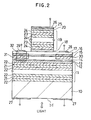
- Fig. 2 is a cross-sectional view of a surface-normal optoelectronic switch device according to a first embodiment of this invention.
- Figs.3 to 5 are for explaining a production method of the device shown in Fig.2 on a processing basis in which;
- Fig.3 cross-sectionally shows that a first semiconductor layer, a second semiconductor layer, an active layer, a third semiconductor layer, a fourth semiconductor layer and a contact layer are formed on a substrate in this order, and that a part of the fourth semiconductor layer and a part of the contact layer are removed thereafter to form a mesa portion thereon.
- Fig.4 cross-sectionally shows that a Zn diffusion region is formed in the third semiconductor layer
- Fig.5 cross-sectionally shows that highly resistant regions are formed in the third semiconductor layer.
- Fig.6 is a cross-sectional view of a surface-normal optoelectronic switch device according to a second embodiment of this invention.
- Fig. 2 cross - sectionally shows a surface - normal optoelectronic switch device according to a first embodiment of this invention.
- a n-type semiconductor multilayer film 11 doping concentration of donor 2 x 10 18 cm -3
- a n-type AlGaAs layer 12 doping concentration of donor 2 x 10 18 cm -3 ; layer thickness 150 nm ; A1 composition ratio 0.4
- a p-type AlGaAs layer 13 doping concentration of acceptor 1 x 10 19 cm -3 ; layer thickness 5 nm ; A1 composition ratio 0.25
- a non-doped AlGaAs layer 14 layer thickness about 100 nm ; A1 composition ratio 0.25
- an active layer 15 having a quantum well structure having laminated a non-doped InGaAs layer (In composition ratio 0.2) and a non-doped AlGaAs layer (A1 composition ratio 0.25) (layer thickness
- the n-type semiconductor multilayer film 11 and n-type AlGaAs layer 12 constitute a first semiconductor layer (cathod region), and the p-type AlGaAs layer 13 constitutes a second semiconductor layer (p-type gate electrode).
- the non-doped AlGaAs layers 14 and 16 each serves to increase a gain of transistor action during the operation of the device.
- the action as the active layer on a strict sense basis is provided by the non-doped InGaAs, and on the other hand, the non-doped AlGaAs layer has the same action as each of the non-doped AlGaAs layers 14 and 16 do.
- the n-type AlGaAs layer 17 constitutes a third semiconductor layer (n-type gate region)
- the p-type AlGaAs layer 18 and p-type semiconductor multilayer film 19 constitute a fourth semiconductor layer (anode region).
- the p-type AlGaAs layer 13 (second semiconductor layer) and n-type AlGaAs layer 17 (third semiconductor layer) having said active layer 15 sandwiched therebetween are made larger in forbidden band width than said active layer 15.
- the forbidden band width of the p-type AlGaAs layer 13 is made smaller than that of the n-type AlGaAs layer 12 (part of the first semiconductor layer) adjacently formed to said layer 13.
- the forbidden band width of the n-type AlGaAs layer 17 is made smaller than that of the p-type AlGaAs layer 18 (part of the fourth semiconductor layer) adjacently formed to said layer 17.
- the n-type semiconductor multilayer film 11 has n-type GaAs layers 21 (layer thickness about 67.2 nm) and n-type AlAs layer 22 (layer thickness about 80.4 nm) alternately laminated.
- n-type GaAs layers 21 layer thickness about 67.2 nm
- n-type AlAs layer 22 layer thickness about 80.4 nm
- 24.5 pairs of the layers 21 and 22 are formed, in other words, 24 n-type AlAs layers 22 and 23 n-type GaAs layers 21 are formed in an alternate lamination manner.
- the p-type semiconductor multilayer film 19 has a p-type GaAs layer 23 (layer thickness about 67.2 nm) and a p-type AlAs layer 24 ( layer thickness about 80.4 nm ) alternately laminated.
- the layer thicknesses shown above correspond to the quarter-wavelengths of a light in respective media (layers).
- the multilayer films 11 and 19 each serves to act as a reflecting film of a light.
- the distance between the films 11 and 19 is preferable to be an integral multiple of the in-medium wavelength of an emitted light in order to make emission easy.
- the distance from the center line of the active lager 15 to the multilayer film 19 is made twice the in-medium wavelength of the emitted light, or about 580 nm, and the distance from the center line of the active layer 15 to the multilayer film 11 is made equal to the in - medium wavelength thereof, or about 290 nm.
- anode electrode consisting of a Cr layer 25 and an Au layer 26 is formed.
- a cathode electrode made of an AuGeNi/Au layer 27 is formed excepting a window (35) formed at the center thereof for taking out a light therefrom.
- the n-type AlGaAs layer 17 is exposed around the cylindrical mesa portion with a diameter of about 10 ⁇ m and on thus exposed surface of the n-type AlGaAs layer 17, a n-type gate electrode 28 made of an AuGeNi/Au layer and a p-type gate electrode 29 made of a Cr/Au layer are formed.
- the n-type gate electrode 28 and p-type gate electrode 29 are disposed on the opposite side to each other with respect to the mesa portion.
- non-doped AlGaAs layer 16 Within the n-type AlGaAs layer 17 (third semiconductor layer), non-doped AlGaAs layer 16, the active layer 15 and non-doped AlGaAs layer 14, as shown in Fig . 2 , high resistance regions 30 and 31 are formed substantially just below the gate electrodes 28 and 29, respectively.
- the high resistance regions 30 and 31 are provided such that in the upper direction, or in the direction perpendicular to the surface of the substrate 10, these regions extend to a portion within the n-type AlGAAs layer 17, that is in the vicinity of the active layer 15, extend through the entire thickness of the non-doped AlGaAs layer 16 and active layer 15 and extend partly into the non-doped AlGaAs layer 14, thus extending a portion of layer 14 on the side of the p-type AlGaAs layer 13 (second semiconductor layer).
- the section of the active layer 15 provided between the high resistance ranges 30 and 31 constitutes a light emitting region.
- a p-type diffusion region 32 having diffused zinc (Zn) atoms is formed passing through the high resistance region 31.
- the p-type diffusion region 32 constitutes a p-type gate region.
- the p-type diffusion region 32 is formed to be attained from the upper surface of the n-type AlGaAs layer 17 to the upper area of the n-type AlGaAs layer 12.
- the n - type semiconductor multilayer film 11 the n-type AlGaAs layer 12, the p-type AlGaAs layer 13, the non-doped AlGaAs layer 14, the active layer 15 of quantum well structure having the non - doped InGaAs layers and non-doped AlGaAs layers laminatedly formed, the non-doped AlGaAs layer 16, the n-type AlGaAs layer 17, the p - type AlGaAs layer 18, the p - type semiconductor multilayer film 19 and the p-type GaAs contact layer 20 are formed in this order by growing epitaxially.
- MBE molecular beam epitaxy
- the p - type GaAs contact layer 20, p-type semiconductor multilayer film 19 and p-type AlGaAs layer 18 are subjected to mesa etching by a lithographic method to form a cylindrical mesa with a diameter of about 10 ⁇ m, which is shown in Fig.3.
- a square pillar-shaped mesa of about 10 ⁇ m square may be formed instead of the cylindrical mesa.
- a SiO 2 film 33 with a thickness of about 0.3 ⁇ m is formed on the surface of said semiconductor multilayer lamination body forming the cylindrical mesa and then, an opening is formed in the SiO 2 film 33 at a predetermined position of the upper surface of the n-type AlGaAs layer 17.
- the diffusion of Zn atoms are carried out at 550 °C.
- the Zn atoms are diffused in the lower direction passing through the opening to form the p-type diffusion region 32 as shown in Fig . 4.
- the diffusion should be carried out so that the diffusion front of the Zn atoms can pass through the p-type AlGaAs layer 13 as the p-type gate region. In this embodiment, the diffusion front is attained to the central portion of the n-type AlGaAs layer 12 formed beneath the p-type AlGaAs layer 13.
- a photoresist film (with a thickness of about 5 ⁇ m) is formed only on the cylindrical mesa of said semiconductor multilayer lamination body and then, the lithography technology is applied to remove the SiO 2 film 33 excepting that formed on the cylindrical mesa.
- a mask consisting of the SiO 2 film 33 and a photoresist film 34 is formed as shown in Fig.5.
- the photoresist film 34 is preferable to be hard-baked for one hour at about 200 °C.
- irradiation of proton (H + ) is made toward said mask to inject the proton thereto from the upper surface of the n-type AlGaAs layer 17 with no mask formed.
- the proton injection is made so as to surround the cylindrical mesa to form an area where the proton is injected. Such a region as is surrounded by the area becomes a light emitting region.
- the proton injection is preferably carried out under the conditions of acceleration voltage 50 keV and dose quantity 3 x 10 14 cm -2 .
- the high resistance regions 30 and 31 can be selectively formed only within the proton-injected layers existing at a moderated depth. Accordingly, there can be formed the high resistance regions 30 and 31 at only the vicinity of the active layer 15.
- the high resistance region 31 is formed inside the p-type diffusion region 32 and the high resistance region 30 is formed outside the same. After proton injection, said mask is removed.
- said semiconductor multilayer lamination body is annealed for thirty seconds at 475 °C.
- the layer 27 made of AuGeNi/Au is formed by the vacuum deposition technology on the lower surface of the substrate 10 except for at the window 35 for extracting light therefrom to make a cathode electrode.
- the Cr layer 25 and the Au layer 26 are laminated in this order by the vacuum deposition technology on the upper surface of the p-type GaAs contact layer 20 to make an anode electrode.
- an AuGeNi/Au layer is formed at a predetermined position of the upper surface of the n-type AlGaAs layer 17 excepting the p-type diffusion range 32 to make the n-type gate electrode 28, and a Cr/Au layer is formed on the upper surface of the n-type AlGaAs layer 17 on the p-type diffusion region 32 to make the p-type gate electrode 29.
- the surface-normal optoelectronic fusion device as shown in Fig.2 can be obtained.
- a bias voltage is applied so as to make the anode electrode positive and the cathode electrode negative, and yet, the value of this bias voltage is set to the value just before the device is turned on.
- the gate electrodes 28 and 29 are not applied with a voltage. Under this condition, if a light is sent from the window formed on the lower surface of the substrate 10 into the device, it is turned on to generate an output light as illustrated. When once turned it on, if the light is stopped to be sent, the turn-on condition is maintained to continue the light emission.
- the polarity of a voltage to be applied to the anode and cathode electrodes is reversed and furthermore, a voltage is applied to the n-type gate electrode 28 and p-type gate electrode 29 so as to make the electrode 28 positive and the electrode 29 negative, respectively.
- the carrier confined into the device is forcibly taken out of it at high speed thereby turning it off.
- the device according to the first embodiment of this invention advantageously features that high speed switching operation can be made while a current level necessary to emit a light under turn-on condition is being maintained low, and that from the fact that it is operable in the LD mode, a luminous efficiency can be improved, a light beam to be emitted is superior in directivity, and yet the compatibility to other devices and optical fibers is outstandingly high.
- a n-type contact layer may be formed between the substrate 10 and the n-type semiconductor multilayer film 11. Therefore, a cathode electrode can be formed on the n-type contact layer thus obtained, so that the electrodes become possible to be formed only on one side of a semiconductor wafer.
- Fig.6 is a cross-sectional view of a surface-normal optoelectronic switch device according to a second embodiment of this invention.
- a n-type AlGaAs layer 41 Al composition ratio 0.4 ; layer thickness 1 ⁇ m; doping concentration of donor 1 x 10 18 cm -3 ), a p-type GaAs layer 42 (layer thickness 5 nm ; doping concentration of acceptor 1 x 10 19 cm -3 ), a n-type GaAs layer 43 (layer thickness 1 ⁇ m; doping concentration of donor 1 x 10 17 cm -3 ), a p-type AlGaAs layer 44 (Al composition ratio 0.4; layer thickness 0.5 ⁇ m ; doping concentration of acceptor 1 x 10 18 cm -3 ) and a p-type GaAs layer 45 (layer thickness 0.2 ⁇ m; doping concentration of acceptor 1 x 10 19 cm -3 ) are laminatedly formed in this order on a n-type GaAs
- the n-type AlGaAs layer 41 constitutes a first semiconductor layer
- the p-type GaAs layer 42 constitutes a second semiconductor layer
- the n-type GaAs layer 43 constitutes a third semiconductor layer
- the p-type AlGaAs layer 44 constitutes a fourth semiconductor layer.
- the p-type GaAs layer 45 is a contact layer.
- the layers 41, 42, 43, 44 and 45 can be successively formed on the substrate 40 by growing epitaxially by a molecular beam epitaxy (MBE) method as in the first embodiment.
- MBE molecular beam epitaxy
- anode electrode 47 is provided on the upper surface of the p-type GaAs contact layer 45 in a mesa portion, an anode electrode 47 is provided, and on the lower surface of the substrate 10, a cathode electrode 46 is provided excepting a window 53 formed at the center thereof for taking out a light therefrom.
- the n-type GaAs layer 43 has the surface exposed around the mesa portion thereby to form a n-type gate electrode 50 and a p-type gate electrode 49 thereon.
- the n-type gate electrode 50 and p-type gate electrode 49 are disposed on the opposite side to each other with respect to the mesa portion.
- n-type GaAs layer 43 third semiconductor layer
- p-type GaAs layer 42 second semiconductor layer
- n-type AlGaAs layer 41 first semiconductor layer
- two high resistance regions 51 and 52 are formed substantially just below the gate electrodes 49 and 50, respectively.
- the high resistance regions 51 and 52 respectively include, in the vertical direction (layer thickness direction), the total thickness of the p-type GaAs layer 42, and the vicinal thickness regions of the n-type GaAs layer 43 and n-type AlGaAs layer 41 to the p-type GaAs layer 42.
- the regions 51 and 52 are not formed in region below said vicinal thickness region of the n-type AlGaAs layer 41 and in the region above said vicinal thickness region of the n-type GaAs layer 43.
- the section of the p-type GaAs layer 42 provided between the high resistance regions 51 and 52 becomes a light emitting region.
- a p-type diffusion region 48 is formed vertically passing through the high resistance region 52 within the n-type GaAs layer 43, p-type GaAs layer 42 and n-type AlGaAs layer 41 as shown in Fig.6, which constitutes a p-type gate region.
- the p-type diffusion range 48 is attained from the upper surface of the n-type Gas layer 43 to the vicinity of the center of the n-type AlGaAs layer 41.
- Said electrodes 46,47,49 and 50, high resistance regions 51 and 52, and p-type diffusion range 48 may be formed by the same method as is used in the first embodiment.
- the p-type GaAs layer 42 and n-type GaAs layer 43 are larger in forbidden band width than the n-type AlGaAs layer 41 and/or p-type AlGaAs layer 44, and the carriers are confined in the p-type GaAs layer 42 and n-type GaAs layer 43 under the turn-on condition, resulting in an improvement in luminous efficiency. As a result, the threshold of luminescence can be reduced.
- the device of this embodiment has a mesa portion as in the first embodiment, which is different therefrom in that the mesa etching is made as to etch the n-type GaAs layer 43 as the third semiconductor layer up to a moderate depth thereby to have the n-type GaAs layer 43 existed at the root of the mesa portion.
- the device of this embodiment is different from that of the preceding embodiment in that the high resistance regions 51 and 52 formed by an ion injection method respectively are provided at the vicinity of the junction of the p-type GaAs layer 42 and n-type GaAs layer 43, and there exists no active layer as formed in the preceding embodiment.
- a method of using the device of this embodiment is the same as in the first embodiment. That is, if it is to be turned on, no voltage applied to the gate electrodes 49 and 50, but a voltage is applied so as to make the anode electrode 47 positive and the cathode electrode 46 negative, and under this condition, a light is sent from the window formed on the lower surface of the substrate 40 thereunto. Thus, a light is emitted from the window on the lower surface of the substrate 40. If it is to be turned off, the polarity of a voltage to be applied to the anode electrode 47 and cathode electrode 46 is reversed, and a voltage is applied thereto so as to make the p-type gate electrode 29 negative and the n-type gate electrode 28 positive.
- the surface-normal optoelectronic switch device of this invention makes it possible to switch it with high speed as well as to provide agood luminous efficiency as compared with conventional ones.
Landscapes
- Physics & Mathematics (AREA)
- Condensed Matter Physics & Semiconductors (AREA)
- General Physics & Mathematics (AREA)
- Electromagnetism (AREA)
- Optics & Photonics (AREA)
- Led Devices (AREA)
- Semiconductor Lasers (AREA)
- Thyristors (AREA)
- Photo Coupler, Interrupter, Optical-To-Optical Conversion Devices (AREA)
Claims (11)
- Dispositif interrupteur optoélectronique émetteur de lumière et récepteur de lumière, vertical à la surface, comprenant :caractérisé en ce queun substrat semi-conducteur (10, 40),une première couche de semi-conducteur (11, 12 ; 41) d'un premier type électroconducteur, formée sur ledit substrat,une seconde couche de semi-conducteur (13 ; 42) d'un second type électroconducteur, ayant une polarité inverse de celle du premier type électroconducteur, qui est formée sur ladite première couche de semi-conducteur,une troisième couche de semi-conducteur (17 ; 43) du premier type électroconducteur, formée sur ladite seconde couche de semi-conducteur,une quatrième couche de semi-conducteur (18, 19 ; 44) du second type électroconducteur, formée sur ladite troisième couche de semi-conducteur,une électrode cathode (27 ; 46) connectée à l'une de ladite première couche de semi-conducteur et de ladite quatrième couche de semi-conducteur,une électrode anode (25, 26 ; 47) connectée à l'autre de ladite première couche de semi-conducteur et de ladite quatrième couche de semi-conducteur,une première électrode de grille (28 ; 49) connectée à ladite seconde couche de semi-conducteur (13 ; 42) etune seconde électrode de grille (29 ; 50) connectée à ladite troisième couche de semi-conducteur, dans lequel ladite seconde (13 ; 42) et ladite troisième (17 ; 43) couches de semi-conducteur ont une plus grande largeur de bande interdite qu'au moins l'une de ladite première couche de semi-conducteur (11 ; 12 ; 41) et de ladite quatrième couche de semi-conducteur (18 ; 19 ; 44),
une région à haute résistance électrique (30, 31 ; 51, 52) est formée à proximité de la jonction desdites seconde (13 ; 42) et troisième (17 ; 43) couches de semi-conducteur, qui entoure une région émettrice de lumière, et qui a une résistance électrique supérieure à celle de la région émettrice de lumière. - Dispositif interrupteur optoélectronique selon la revendication 1, dans lequel une couche active de semi-conducteur (15) est formée entre ladite seconde couche de semi-conducteur (13) et ladite troisième couche de semi-conducteur (17) ; dans lequel ladite seconde (13) et ladite troisième (17) couches de semi-conducteur ont une plus grande largeur de bande interdite que ladite couche active de semi-conducteur (15), ladite seconde couche de semi-conducteur (13) a une plus petite largeur de bande interdite qu'au moins la partie de ladite première couche de semi-conducteur (11, 12) qui est en contact avec ladite seconde couche de semi-conducteur (13), et ladite troisième couche de semi-conducteur (17) a une plus petite largeur de bande interdite qu'au moins la partie de ladite quatrième couche de semi-conducteur (18, 19) qui est en contact avec ladite troisième couche de semi-conducteur (17), et ladite région à haute résistance électrique (30, 31) passe verticalement à travers ladite couche active (15) et entoure une région émettrice de ladite couche active.
- Dispositif interrupteur optoélectronique selon la revendication 1 ou 2, dans lequel une fenêtre (35 ; 53) est placée sur une face dudit substrat semi-conducteur (10 ; 40) qui est opposée à ladite première couche de semi-conducteur (11,12 ; 41), de sorte que la lumière est émise et reçue à travers ladite fenêtre (35 ; 53).
- Dispositif interrupteur optoélectronique selon la revendication 2 ou 3, dans lequel ladite première couche de semi-conducteur (11, 12) comprend une couche qui sert de miroir réflecteur, et ladite quatrième couche de semi-conducteur (18, 19) comprend une couche qui sert de miroir réflecteur.
- Dispositif interrupteur optoélectronique selon la revendication 4, dans lequel lesdites couches qui servent desdits miroirs réflecteurs sont des films multicouches, respectivement.
- Dispositif interrupteur optoélectronique selon la revendication 2 ou 5, dans lequel une épaisseur totale de ladite seconde couche de semi-conducteur (13), de ladite couche active de semi-conducteur (15) et de ladite troisième couche de semi-conducteur (17) est égale à un multiple entier d'une longueur d'onde moyenne de lumière émise par la région émettrice de lumière.
- Dispositif interrupteur optoélectronique selon la revendication 6, comprenant en outre une partie mésa, dans lequel ladite quatrième couche de semi-conducteur (18, 19) est formée dans ladite partie mésa, et ladite région à haute résistance (30, 31) est formée autour de ladite partie mésa.
- Dispositif interrupteur optoélectronique selon la revendication 7, dans lequel ladite région à haute résistance (30, 31) s'étend au moins dans l'une de ladite seconde couche de semi-conducteur (13) et de ladite troisième couche de semi-conducteur (17).
- Dispositif interrupteur optoélectronique selon la revendication 1, comprenant en outre une partie mésa, dans lequel la totalité de ladite quatrième couche de semi-conducteur (44) et une partie de ladite troisième couche de semi-conducteur (43) sont formées dans ladite partie mésa, et ladite région à haute résistance (31, 51) est formée autour de ladite partie mésa.
- Dispositif interrupteur optoélectronique selon la revendication 9, dans lequel ladite région à haute résistance (51, 52) s'étend jusqu'à ladite première couche de semi-conducteur (41) et ladite troisième couche de semi-conducteur (43).
- Méthode de fabrication d'un dispositif interrupteur optoélectronique selon la revendication 1 ou 2, dans laquelle ladite région à haute résistance (30, 31 ; 51, 52) est formée sélectivement par une technique d'implantation ionique.
Applications Claiming Priority (2)
| Application Number | Priority Date | Filing Date | Title |
|---|---|---|---|
| JP34754/91 | 1991-02-28 | ||
| JP3475491A JP2710171B2 (ja) | 1991-02-28 | 1991-02-28 | 面入出力光電融合素子 |
Publications (3)
| Publication Number | Publication Date |
|---|---|
| EP0501246A2 EP0501246A2 (fr) | 1992-09-02 |
| EP0501246A3 EP0501246A3 (en) | 1993-01-20 |
| EP0501246B1 true EP0501246B1 (fr) | 1998-05-27 |
Family
ID=12423110
Family Applications (1)
| Application Number | Title | Priority Date | Filing Date |
|---|---|---|---|
| EP92102438A Expired - Lifetime EP0501246B1 (fr) | 1991-02-28 | 1992-02-13 | Dispositif interrupteur optoélectronique |
Country Status (5)
| Country | Link |
|---|---|
| US (1) | US5340998A (fr) |
| EP (1) | EP0501246B1 (fr) |
| JP (1) | JP2710171B2 (fr) |
| CA (1) | CA2061349C (fr) |
| DE (1) | DE69225632T2 (fr) |
Families Citing this family (13)
| Publication number | Priority date | Publication date | Assignee | Title |
|---|---|---|---|---|
| US5729566A (en) * | 1996-06-07 | 1998-03-17 | Picolight Incorporated | Light emitting device having an electrical contact through a layer containing oxidized material |
| JP2000056281A (ja) * | 1998-08-07 | 2000-02-25 | Mitsubishi Electric Corp | 光変調器とその製造方法 |
| JP2001189526A (ja) * | 2000-01-05 | 2001-07-10 | Nippon Sheet Glass Co Ltd | 自己走査型面発光レーザアレイ |
| US6674785B2 (en) | 2000-09-21 | 2004-01-06 | Ricoh Company, Ltd. | Vertical-cavity, surface-emission type laser diode and fabrication process thereof |
| US6479844B2 (en) * | 2001-03-02 | 2002-11-12 | University Of Connecticut | Modulation doped thyristor and complementary transistor combination for a monolithic optoelectronic integrated circuit |
| JP3760235B2 (ja) * | 2003-04-04 | 2006-03-29 | 独立行政法人 宇宙航空研究開発機構 | 半導体レーザ及び半導体レーザの発振方法 |
| US7772615B2 (en) * | 2007-08-10 | 2010-08-10 | Connector Optics | Anti stark electrooptic medium and electrooptically modulated optoelectronic device based thereupon |
| JP4595012B2 (ja) * | 2008-03-26 | 2010-12-08 | 株式会社沖データ | 半導体発光装置、光プリントヘッド、および画像形成装置 |
| JP5665504B2 (ja) * | 2010-11-24 | 2015-02-04 | キヤノン株式会社 | 垂直共振器型面発光レーザおよび垂直共振器型面発光レーザアレイ |
| JP2012204677A (ja) * | 2011-03-25 | 2012-10-22 | Fuji Xerox Co Ltd | 発光サイリスタ、光源ヘッド、及び画像形成装置 |
| JP7216270B2 (ja) * | 2018-09-28 | 2023-02-01 | 日亜化学工業株式会社 | 半導体発光素子 |
| CN113381297B (zh) * | 2020-03-09 | 2022-07-01 | 济南晶正电子科技有限公司 | 一种集成光学复合基板 |
| CN118801218B (zh) * | 2024-07-11 | 2025-03-28 | 天津赛米卡尔科技有限公司 | 一种具有双栅控制的半导体激光器结构及制备方法 |
Family Cites Families (13)
| Publication number | Priority date | Publication date | Assignee | Title |
|---|---|---|---|---|
| FR2273371B1 (fr) * | 1974-05-28 | 1978-03-31 | Thomson Csf | |
| FR2396419A1 (fr) * | 1977-06-27 | 1979-01-26 | Thomson Csf | Diode capable de fonctionner en emetteur et detecteur de lumiere de la meme longueur d'onde alternativement |
| US4216485A (en) * | 1978-09-15 | 1980-08-05 | Westinghouse Electric Corp. | Optical transistor structure |
| US4450567A (en) * | 1979-07-12 | 1984-05-22 | Xerox Corporation | Optical repeater integrated lasers |
| JPH0738457B2 (ja) * | 1986-07-18 | 1995-04-26 | 株式会社東芝 | 光・電子双安定素子 |
| JPS6373688A (ja) * | 1986-09-17 | 1988-04-04 | Mitsubishi Electric Corp | 半導体発光装置 |
| JPS63200131A (ja) * | 1987-02-17 | 1988-08-18 | Nec Corp | 光論理素子 |
| JPS6414963A (en) * | 1987-07-08 | 1989-01-19 | Nec Corp | Pnpn semiconductor element |
| JPS6488518A (en) * | 1987-09-30 | 1989-04-03 | Hitachi Ltd | Semiconductor device for controlling beam of light |
| US5038356A (en) * | 1989-12-04 | 1991-08-06 | Trw Inc. | Vertical-cavity surface-emitting diode laser |
| JP2898347B2 (ja) * | 1990-04-23 | 1999-05-31 | イーストマン・コダックジャパン株式会社 | 発光ダイオードアレイ |
| US5068868A (en) * | 1990-05-21 | 1991-11-26 | At&T Bell Laboratories | Vertical cavity surface emitting lasers with electrically conducting mirrors |
| US5063569A (en) * | 1990-12-19 | 1991-11-05 | At&T Bell Laboratories | Vertical-cavity surface-emitting laser with non-epitaxial multilayered dielectric reflectors located on both surfaces |
-
1991
- 1991-02-28 JP JP3475491A patent/JP2710171B2/ja not_active Expired - Fee Related
-
1992
- 1992-02-13 DE DE69225632T patent/DE69225632T2/de not_active Expired - Fee Related
- 1992-02-13 EP EP92102438A patent/EP0501246B1/fr not_active Expired - Lifetime
- 1992-02-17 CA CA002061349A patent/CA2061349C/fr not_active Expired - Fee Related
- 1992-02-28 US US07/843,212 patent/US5340998A/en not_active Expired - Fee Related
Non-Patent Citations (1)
| Title |
|---|
| (LEOS), Boston, MA, 4th-9th November 1990, pages 655-656; M. SUGIMOTO et al.: "Surface-emitting-laser operation in vertical to surface transmission electro- photonic devices with a vertical cavity" * |
Also Published As
| Publication number | Publication date |
|---|---|
| JP2710171B2 (ja) | 1998-02-10 |
| US5340998A (en) | 1994-08-23 |
| CA2061349C (fr) | 1996-11-05 |
| JPH07240506A (ja) | 1995-09-12 |
| EP0501246A2 (fr) | 1992-09-02 |
| CA2061349A1 (fr) | 1992-08-29 |
| DE69225632T2 (de) | 1999-02-25 |
| EP0501246A3 (en) | 1993-01-20 |
| DE69225632D1 (de) | 1998-07-02 |
Similar Documents
| Publication | Publication Date | Title |
|---|---|---|
| US6936486B2 (en) | Low voltage multi-junction vertical cavity surface emitting laser | |
| US5892787A (en) | N-drive, p-common light-emitting devices fabricated on an n-type substrate and method of making same | |
| US6175582B1 (en) | Semiconductor laser device | |
| US5034958A (en) | Front-surface emitting diode laser | |
| US5212706A (en) | Laser diode assembly with tunnel junctions and providing multiple beams | |
| US6169756B1 (en) | Vertical cavity surface-emitting laser with optical guide and current aperture | |
| EP0609836B1 (fr) | Laser à émission de surface et son procédé de fabrication | |
| US4829357A (en) | PNPN thyristor | |
| US5455429A (en) | Semiconductor devices incorporating p-type and n-type impurity induced layer disordered material | |
| EP0474018B1 (fr) | Dispositif électrophotonique à cavité verticale du type transmission verticale vers la surface | |
| US6570905B1 (en) | Vertical cavity surface emitting laser with reduced parasitic capacitance | |
| EP0288267B1 (fr) | Dispositif optique à semi-conducteur | |
| EP0501246B1 (fr) | Dispositif interrupteur optoélectronique | |
| US5608753A (en) | Semiconductor devices incorporating p-type and n-type impurity induced layer disordered material | |
| JP3016302B2 (ja) | pnpn半導体素子とその駆動回路 | |
| US5432809A (en) | VCSEL with Al-free cavity region | |
| US5574745A (en) | Semiconductor devices incorporating P-type and N-type impurity induced layer disordered material | |
| EP0791990A1 (fr) | VCSEL à nervure à faible résistance du type p en bas et méthode de fabrication | |
| US6770915B2 (en) | Light emitting element with multiple multi-layer reflectors and a barrier layers | |
| JPH06196804A (ja) | 面発光型半導体レーザ素子 | |
| JP3228384B2 (ja) | 光スイッチアレイ | |
| TW202339377A (zh) | Vcsel、帶有vcsel的用於發送光學信號脈衝的發送器、操作vcsel之方法及製造vcsel之方法 | |
| JPS63211785A (ja) | 多重量子井戸型光双安定半導体レ−ザ | |
| JPH0680866B2 (ja) | 半導体光メモリ | |
| GB2283612A (en) | Semiconductor laser device |
Legal Events
| Date | Code | Title | Description |
|---|---|---|---|
| PUAI | Public reference made under article 153(3) epc to a published international application that has entered the european phase |
Free format text: ORIGINAL CODE: 0009012 |
|
| 17P | Request for examination filed |
Effective date: 19920325 |
|
| AK | Designated contracting states |
Kind code of ref document: A2 Designated state(s): DE FR GB |
|
| PUAL | Search report despatched |
Free format text: ORIGINAL CODE: 0009013 |
|
| AK | Designated contracting states |
Kind code of ref document: A3 Designated state(s): DE FR GB |
|
| 17Q | First examination report despatched |
Effective date: 19940704 |
|
| GRAG | Despatch of communication of intention to grant |
Free format text: ORIGINAL CODE: EPIDOS AGRA |
|
| GRAG | Despatch of communication of intention to grant |
Free format text: ORIGINAL CODE: EPIDOS AGRA |
|
| GRAH | Despatch of communication of intention to grant a patent |
Free format text: ORIGINAL CODE: EPIDOS IGRA |
|
| GRAH | Despatch of communication of intention to grant a patent |
Free format text: ORIGINAL CODE: EPIDOS IGRA |
|
| GRAA | (expected) grant |
Free format text: ORIGINAL CODE: 0009210 |
|
| AK | Designated contracting states |
Kind code of ref document: B1 Designated state(s): DE FR GB |
|
| REF | Corresponds to: |
Ref document number: 69225632 Country of ref document: DE Date of ref document: 19980702 |
|
| ET | Fr: translation filed | ||
| PLBE | No opposition filed within time limit |
Free format text: ORIGINAL CODE: 0009261 |
|
| STAA | Information on the status of an ep patent application or granted ep patent |
Free format text: STATUS: NO OPPOSITION FILED WITHIN TIME LIMIT |
|
| 26N | No opposition filed | ||
| REG | Reference to a national code |
Ref country code: GB Ref legal event code: IF02 |
|
| PGFP | Annual fee paid to national office [announced via postgrant information from national office to epo] |
Ref country code: FR Payment date: 20040210 Year of fee payment: 13 |
|
| PGFP | Annual fee paid to national office [announced via postgrant information from national office to epo] |
Ref country code: GB Payment date: 20040211 Year of fee payment: 13 |
|
| PGFP | Annual fee paid to national office [announced via postgrant information from national office to epo] |
Ref country code: DE Payment date: 20040226 Year of fee payment: 13 |
|
| PG25 | Lapsed in a contracting state [announced via postgrant information from national office to epo] |
Ref country code: GB Free format text: LAPSE BECAUSE OF NON-PAYMENT OF DUE FEES Effective date: 20050213 |
|
| PG25 | Lapsed in a contracting state [announced via postgrant information from national office to epo] |
Ref country code: DE Free format text: LAPSE BECAUSE OF NON-PAYMENT OF DUE FEES Effective date: 20050901 |
|
| GBPC | Gb: european patent ceased through non-payment of renewal fee |
Effective date: 20050212 |
|
| PG25 | Lapsed in a contracting state [announced via postgrant information from national office to epo] |
Ref country code: FR Free format text: LAPSE BECAUSE OF NON-PAYMENT OF DUE FEES Effective date: 20051031 |
|
| REG | Reference to a national code |
Ref country code: FR Ref legal event code: ST Effective date: 20051031 |