EP0116820A2 - Komplementäre MOS-Schaltung - Google Patents
Komplementäre MOS-Schaltung Download PDFInfo
- Publication number
- EP0116820A2 EP0116820A2 EP84100033A EP84100033A EP0116820A2 EP 0116820 A2 EP0116820 A2 EP 0116820A2 EP 84100033 A EP84100033 A EP 84100033A EP 84100033 A EP84100033 A EP 84100033A EP 0116820 A2 EP0116820 A2 EP 0116820A2
- Authority
- EP
- European Patent Office
- Prior art keywords
- voltages
- channel mos
- power supply
- mos transistor
- terminal
- Prior art date
- Legal status (The legal status is an assumption and is not a legal conclusion. Google has not performed a legal analysis and makes no representation as to the accuracy of the status listed.)
- Granted
Links
Images



Classifications
-
- G—PHYSICS
- G05—CONTROLLING; REGULATING
- G05F—SYSTEMS FOR REGULATING ELECTRIC OR MAGNETIC VARIABLES
- G05F3/00—Non-retroactive systems for regulating electric variables by using an uncontrolled element, or an uncontrolled combination of elements, such element or such combination having self-regulating properties
- G05F3/02—Regulating voltage or current
- G05F3/08—Regulating voltage or current wherein the variable is DC
- G05F3/10—Regulating voltage or current wherein the variable is DC using uncontrolled devices with non-linear characteristics
- G05F3/16—Regulating voltage or current wherein the variable is DC using uncontrolled devices with non-linear characteristics being semiconductor devices
- G05F3/20—Regulating voltage or current wherein the variable is DC using uncontrolled devices with non-linear characteristics being semiconductor devices using diode- transistor combinations
- G05F3/205—Substrate bias-voltage generators
-
- H—ELECTRICITY
- H10—SEMICONDUCTOR DEVICES; ELECTRIC SOLID-STATE DEVICES NOT OTHERWISE PROVIDED FOR
- H10D—INORGANIC ELECTRIC SEMICONDUCTOR DEVICES
- H10D89/00—Aspects of integrated devices not covered by groups H10D84/00 - H10D88/00
- H10D89/211—Design considerations for internal polarisation
- H10D89/213—Design considerations for internal polarisation in field-effect devices
Definitions
- the present invention relates to a semiconductor device in which a complementary MOS circuit is formed on a semiconductor substrate.
- CMOS-LSIs have attracted much attention because of their low power consumption so that they will be widely used in various fields.
- problems which may be summarized as follows:
- One of the objects of the present invention is to provide a semiconductor device in.which the value of the parasitic junction capacitance between a substrate, a source and a drain of each of PMOS transistors and NMO S transistors is decreased so that the high speed or faster operation can be attained.
- Another object of the present invention is to provide a semiconductor device in which a PNPN switch formed between the substrate and the source of each PMOS and NMOS transistors can be prevented from being turned on so that latch-up susceptibility can be minimized.
- a further object of the present invention is to provide a semiconductor device in which an element is reduced in dimension by scaling so that the high speed or faster operation may be ensured.
- a yet further object of the present invention is to provide a semiconductor device whose performance is not adversely affected by the variations in external power supply and whose operational margin may be improved.
- the present invention provides a semiconductor device in which the gates of a NMOS transistor and a PMOS transistor, which constitute a CMOS circuit on a semiconductor substrate of one type or polarity, are connected in common to an input terminal while the drains thereof are connected in common to an output terminal; internal power supply means (whose output voltages are V 3 and V 4 respectively) are provided which respond to externally supplied voltages (V 1 and V 2 ) so as to deliver the output voltages V 3 and V 4 (which will not vary in response to the variations in externally supplied voltages V 1 and V 2 ); the voltages V 1 , V 2' V 3 and V 4 are applied to the substrate terminal of the NMOS transistor, the substrate terminal of the PMOS transistor, the source terminal of the NMOS transistor and the source terminal of the PMOS transistor, respectively; and in order to apply a predetermined bias voltage across each junction of these MOS transistors, the following relationship is maintained among the voltages V 1 , V 2 , V 3 and V 4 : where V 1 may be
- CMOS inverter Prior to the description of the preferred embodiments of the present invention, a conventional CMOS inverter will be briefly described with reference to FIG. 8 so that the problems encountered in the conventional CMOS devices may be more particularly pointed out.
- the CMOS inverter as shown in FIG. 8 comprises an n-channel MOS transistor 1 (to be referred as “NMOS transistor” in this specification) and a p-channel MOS transistor 2 (to be referred as "PMOS txansistor” in this specification).
- NMOS transistor n-channel MOS transistor 1
- PMOS txansistor p-channel MOS transistor 2
- Gate terminals 101 and 201 of NMOS and PMOS transistors 1 and 2 are connected in common to an input terminal IN while drains 102 and 202 of NMOS and PMOS transistors 1 and 2 are connected in common to an output terminal OUT.
- the source terminal 103 and the substrate terminal 104 of NMOS transistor 1 is connected in common to an external reference power supply Vss which supplies the power to an LSI chip.
- the source terminal 203 and the substrate terminal 204 of PMOS transistor 2 are connected in common to an external power supply Vcc.
- the conventional CMOS inverter with the above-described construction has the following problems.
- each of the substrates of PMOS and NMOS transistors which constitute a CMOS circuit, is connected not only to the external power supply terminal Vcc but also to the external reference power supply terminal Vss so that the parasitic capacitance between the substrate, source and drain of each of PMOS and NMOS transistors.
- the high speed operation cannot be attained.
- the potential of the source is the same as the potential of the substrate.
- a PNPN switch made up of the source P and the substrate N of the PMOS transistor and the substrate P and the source N + of NMOS transistor is turned on so that the latch-up condition which is similar to that encountered in a thyristor results.
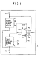
- FIGS. 1 through 7B the preferred embodiments of the present invention will be described.
- a first internal power supply 5 and a second internal power supply 6 are formed over a semiconductor substrate 3.
- the first and second internal power supplies 5 and 6 convert first and second external voltages V 1 and V 2 supplied at first and second external power supply terminals 51 and 61, respectively, into first and second internal voltages V 3 and V 4 , respectively.
- the voltages V 3 and V 4 are applied through internal voltage terminals 52 and 62, respectively, to the source terminals 103 and 203, respectively, of the NMOS and PMOS transistors 1 and 2.
- the first and second external voltages V 1 and V 2 are applied to the substrate terminals 104 and 204 of the NMOS and PMOS transistors 1 and 2.
- the voltages are applied to the CMOS inverter 4 in the manner described above so that the substrate bias voltage of 1V is applied across the source terminal 103 and the substrate terminal 104 of the NMOS transistor 1.
- the substrate bias voltage of 1V is applied across the source terminal 203 and the substrate terminal 204 of the PMOS transistor 2.
- the value of the parasitic junction capacitance of the CMOS inverter 4 is remarkably decreased so that high speed operation can be attained.
- the PN junctions of the PNPN switch made up of the source P + and the substrate N of the PMOS transistor 2 and the substrate P and the source N + of the NMOS transistor are reverse biased so that the latch-up condition due to external causes can be almost avoided.
- the first and second internal power supplies 5 and 6 supply the voltages V 3 and V 4 .
- the package density of circuits can be considerably increased while the externally supplied voltages are maintained constant.
- the operation of the CMOS inverter 4 is not adversely affected by the variations in externally supplied voltage.
- the CMOS inverter 4 In response to the input signal whose amplitude varies between V 1 and V or between V 3 and V 4 , the CMOS inverter 4 delivers the output whose amplitude is varied between V 3 and V 4' the amplitude being reversed.
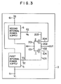
- the second internal power supply 6 converts the externally supplied voltages V 1 and V 2 into a second internally supplied voltage V 4 which in turn is delivered through the terminal 62.
- the first internal power supply 5 converts the first externally supplied voltage V 1 and the output V 4 of the second internal power supply 6 into a second internally supplied voltage V 3 which in turn is delivered through the terminal 52.
- the externally supplied voltages and the internally supplied voltages have the same relationship as the first embodiment; that is,
- the first internal power supply 5 converts the first and second externally supplied voltages V 1 and V 2 into a first internally supplied voltage V 3 which in turn is delivered through the terminal 52.
- the second internal power supply 6 converts the second externally supplied voltage V 2 and the output V 3 of the first internal power supply 5 into a second internally delivered voltage V 4 which in turn is delivered through the terminal 62.
- the following relationship is held:
- FIG. 4 shows in detail the first and second internal power supplies 5 and 6 as shown in Fig. 2.
- the first externally supplied voltage V 1 is applied to the source terminals of NMOS transistors 7 and 8.
- the NMOS transistor 7 and a PMOS transistor 9 constitute a CMOS inverter the output of which is applied to the gate terminal of the NMOS transistor 8 through a NOT gate G 1 .
- the input to the CMOS inverter is the output from a constant voltage circuit consisting of diodes D 1 , D 2 , D3 and D 4 and a resistor R l .
- the first internal power supply 5 detects whether the voltage at the terminal 52 is higher or lower than a threshold value and the detected output voltage is fed back so that a predetermined voltage is produced.
- the second ,internally supplied voltage V 4 is applied to the source terminal of the PMOS transistor 9 and one end of the resistor R 1 .
- the drain terminal of the NMOS transistor with a high mutual conductance gm is connected to the cathode of the diode D 4 and to the terminal 52.
- the first internally supplied voltage V 3 is delivered through the terminal 52.
- the second externally supplied voltage V 2 is applied through the terminal 61 to the source terminals of PMOS transistors 10 and 11.
- the PMOS transistor 10 and a NMOS transistor 12 constitute a CMOS inverter whose output is delivered through a NOT gate G 2 to the gate terminal of the PMOS transistor 11.
- the input to the CMOS inverter is the output of a constant voltage circuit comprising diodes D 5 through D 10 and a resistor R 2 .
- the first externally supplied voltage V 1 is applied to the source terminal of the NMOS transistor 12 and one end of the resistor R 2 .
- the drain terminal of the PMOS transistor with a high mutual conductance gm is connected to the anode of the diode D 10 and the terminal 62.
- the second internally supplied voltage V 4 is delivered through the terminal 62.
- Both the first and second internal power supplies 5 and 6 have a feedback loop so that a stabilized constant voltage output can be obtained.
- FIGS. 6A and 6B show in detail a MOS integrated circuit 30 shown in FIG. 5.
- FIG. 6A shows a NAND gate comprising PMOS transistors 21 and 22 and NMOS transistors 23 and 24 while
- FIG. 6B shows a NOR gate consisting of PMOS transistors 25 and 26 and NMOS transistors 27 and 28.
- the input signal is applied to terminals IN 1 and IN 2 while the output signal is derived from an output terminal OUT.
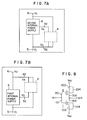
- FIGS. 7A and 7B show the fourth embodiment of the present invention in which the first or the second internal power supply is eliminated. More particularly, in FIG. 7A, a first internal power supply is eliminated and the first externally supplied voltage terminal 51 is directly connected to the first internally supplied voltage terminal 52. In FIG. 7B, a second internal power supply is eliminated and the second externally supplied voltage terminal 61 is directly connected to the second internally supplied voltage terminal 62.
- the externally and internally supplied voltages have the following relationship:
- the externally and internally supplied voltages have the following relationship: Therefore the variations in externally supplied voltage affect one of a pair of MOS transistors of a CMOS, but the other MOS transistor receives a predetermined voltage so that no adverse problem will result in practice.
- the present invention can provide a semiconductor device which has the following effects.
- V 1 may be equal to V 3 or V 4 may be equal to V 2
- V 4 may be equal to V 2
- V 1 may be equal to V 3 or V 4 may be equal to V 2
- V 4 may be equal to V 2
- V 1 may be equal to V 3 or V 4 may be equal to V 2
- V 2 5V
Landscapes
- Engineering & Computer Science (AREA)
- Physics & Mathematics (AREA)
- Microelectronics & Electronic Packaging (AREA)
- Nonlinear Science (AREA)
- Electromagnetism (AREA)
- General Physics & Mathematics (AREA)
- Radar, Positioning & Navigation (AREA)
- Automation & Control Theory (AREA)
- Logic Circuits (AREA)
- Metal-Oxide And Bipolar Metal-Oxide Semiconductor Integrated Circuits (AREA)
- Electronic Switches (AREA)
Applications Claiming Priority (2)
| Application Number | Priority Date | Filing Date | Title |
|---|---|---|---|
| JP58027470A JPS59153331A (ja) | 1983-02-21 | 1983-02-21 | 半導体装置 |
| JP27470/83 | 1983-02-21 |
Publications (3)
| Publication Number | Publication Date |
|---|---|
| EP0116820A2 true EP0116820A2 (de) | 1984-08-29 |
| EP0116820A3 EP0116820A3 (en) | 1986-06-25 |
| EP0116820B1 EP0116820B1 (de) | 1989-03-22 |
Family
ID=12221993
Family Applications (1)
| Application Number | Title | Priority Date | Filing Date |
|---|---|---|---|
| EP84100033A Expired EP0116820B1 (de) | 1983-02-21 | 1984-01-03 | Komplementäre MOS-Schaltung |
Country Status (4)
| Country | Link |
|---|---|
| US (1) | US4837460A (de) |
| EP (1) | EP0116820B1 (de) |
| JP (1) | JPS59153331A (de) |
| DE (1) | DE3477448D1 (de) |
Cited By (8)
| Publication number | Priority date | Publication date | Assignee | Title |
|---|---|---|---|---|
| EP0602268A1 (de) * | 1992-12-16 | 1994-06-22 | Landis & Gyr Business Support AG | Integrierte Schaltung mit Feldeffekt-Transistoren |
| WO1995019046A1 (en) * | 1994-01-10 | 1995-07-13 | Carnegie Mellon University | Four rail circuit architecture for ultra-low power and voltage cmos circuit design |
| EP0545604A3 (de) * | 1991-11-29 | 1995-11-22 | Fuji Electric Co. Ltd. | Integrierte Schaltung mit einer hohen Spannungsfestigkeit |
| GB2300531A (en) * | 1995-05-02 | 1996-11-06 | Plessey Semiconductors Ltd | Reduced swing CMOS output buffer |
| US5814845A (en) * | 1995-01-10 | 1998-09-29 | Carnegie Mellon University | Four rail circuit architecture for ultra-low power and voltage CMOS circuit design |
| GB2349998A (en) * | 1996-05-28 | 2000-11-15 | Altera Corp | A level converter and output driver with separate noisy and quiet supplies |
| US6366061B1 (en) | 1999-01-13 | 2002-04-02 | Carnegie Mellon University | Multiple power supply circuit architecture |
| WO2014122467A1 (en) | 2013-02-06 | 2014-08-14 | Loxbridge Research Llp | Systems and methods for early disease detection and real-time disease monitoring |
Families Citing this family (28)
| Publication number | Priority date | Publication date | Assignee | Title |
|---|---|---|---|---|
| JPH0754628B2 (ja) * | 1985-09-30 | 1995-06-07 | 株式会社東芝 | 半導体装置 |
| USRE40132E1 (en) | 1988-06-17 | 2008-03-04 | Elpida Memory, Inc. | Large scale integrated circuit with sense amplifier circuits for low voltage operation |
| JP2569777B2 (ja) * | 1988-12-16 | 1997-01-08 | 日本電気株式会社 | 入力信号切り換え回路 |
| US5079441A (en) * | 1988-12-19 | 1992-01-07 | Texas Instruments Incorporated | Integrated circuit having an internal reference circuit to supply internal logic circuits with a reduced voltage |
| US4958086A (en) * | 1989-05-08 | 1990-09-18 | Motorola, Inc. | Low di/dt output buffer with improved speed |
| US5128560A (en) * | 1991-03-22 | 1992-07-07 | Micron Technology, Inc. | Boosted supply output driver circuit for driving an all N-channel output stage |
| US5160855A (en) * | 1991-06-28 | 1992-11-03 | Digital Equipment Corporation | Floating-well CMOS output driver |
| CN1075690C (zh) * | 1991-11-07 | 2001-11-28 | 摩托罗拉公司 | 混合信号处理系统及其供电方法 |
| EP0564204A3 (en) * | 1992-03-30 | 1994-09-28 | Mitsubishi Electric Corp | Semiconductor device |
| US5329184A (en) * | 1992-11-05 | 1994-07-12 | National Semiconductor Corporation | Method and apparatus for feedback control of I/O characteristics of digital interface circuits |
| US5371419A (en) * | 1992-11-23 | 1994-12-06 | Mitsubishi Denki Kabushiki Kaisha | CMOS well switching circuit |
| US5338978A (en) * | 1993-02-10 | 1994-08-16 | National Semiconductor Corporation | Full swing power down buffer circuit with multiple power supply isolation |
| JPH0974347A (ja) * | 1995-06-26 | 1997-03-18 | Mitsubishi Electric Corp | Mos集積回路 |
| JP4036487B2 (ja) | 1995-08-18 | 2008-01-23 | 株式会社ルネサステクノロジ | 半導体記憶装置、および半導体回路装置 |
| US6175952B1 (en) | 1997-05-27 | 2001-01-16 | Altera Corporation | Technique of fabricating integrated circuits having interfaces compatible with different operating voltage conditions |
| US6118302A (en) | 1996-05-28 | 2000-09-12 | Altera Corporation | Interface for low-voltage semiconductor devices |
| US6025737A (en) * | 1996-11-27 | 2000-02-15 | Altera Corporation | Circuitry for a low internal voltage integrated circuit |
| JP3266527B2 (ja) * | 1996-12-10 | 2002-03-18 | 富士通株式会社 | 出力ドライバ回路及び半導体装置 |
| JP3732914B2 (ja) | 1997-02-28 | 2006-01-11 | 株式会社ルネサステクノロジ | 半導体装置 |
| US6239612B1 (en) | 1997-08-20 | 2001-05-29 | Altera Corporation | Programmable I/O cells with multiple drivers |
| US6087885A (en) * | 1997-09-11 | 2000-07-11 | Mitsubishi Denki Kabushiki Kaisha | Semiconductor device allowing fast and stable transmission of signals |
| TW462143B (en) * | 1997-09-11 | 2001-11-01 | Mitsubishi Electric Corp | Semiconductor integrated circuit |
| JP3542476B2 (ja) * | 1997-12-01 | 2004-07-14 | 三菱電機株式会社 | Soi構造のcmos回路 |
| US5988819A (en) * | 1998-02-17 | 1999-11-23 | Maxim Integrated Products, Inc. | Single output transistor output stage for interface applications |
| US6680650B2 (en) | 2001-01-12 | 2004-01-20 | Broadcom Corporation | MOSFET well biasing scheme that migrates body effect |
| US20080166524A1 (en) * | 2007-01-02 | 2008-07-10 | Polyworks, Inc. | Thermoformed cushioning material and method of making |
| US7868667B2 (en) * | 2008-03-26 | 2011-01-11 | Hynix Semiconductor Inc. | Output driving device |
| KR101699033B1 (ko) * | 2009-11-30 | 2017-01-24 | 에스케이하이닉스 주식회사 | 출력 드라이버 |
Family Cites Families (15)
| Publication number | Priority date | Publication date | Assignee | Title |
|---|---|---|---|---|
| US3855549A (en) * | 1973-08-24 | 1974-12-17 | Rca Corp | Circuit, such as cmos crystal oscillator, with reduced power consumption |
| US4006491A (en) * | 1975-05-15 | 1977-02-01 | Motorola, Inc. | Integrated circuit having internal main supply voltage regulator |
| US4209713A (en) * | 1975-07-18 | 1980-06-24 | Tokyo Shibaura Electric Co., Ltd. | Semiconductor integrated circuit device in which difficulties caused by parasitic transistors are eliminated |
| US4039869A (en) * | 1975-11-28 | 1977-08-02 | Rca Corporation | Protection circuit |
| JPS5318377A (en) * | 1976-08-03 | 1978-02-20 | Toshiba Corp | Logical operation circuit |
| JPS5323555A (en) * | 1976-08-17 | 1978-03-04 | Nec Corp | Complemen tary mos integrated circuit |
| JPS6042621B2 (ja) * | 1977-03-31 | 1985-09-24 | 株式会社東芝 | Mos集積回路装置 |
| JPS5935217B2 (ja) * | 1977-03-31 | 1984-08-27 | シャープ株式会社 | C−mos回路 |
| JPS54159158A (en) * | 1978-06-06 | 1979-12-15 | Nec Corp | Field effect transistor circuit |
| JPS5516539A (en) * | 1978-07-20 | 1980-02-05 | Nec Corp | Level shifter circuit |
| JPS5591861A (en) * | 1978-12-29 | 1980-07-11 | Fujitsu Ltd | Cmos logic circuit |
| JPS582061B2 (ja) * | 1980-03-05 | 1983-01-13 | 株式会社新潟鐵工所 | 多成分液状プラスチツク原料混合装置の原料供給装置 |
| US4482985A (en) * | 1981-04-17 | 1984-11-13 | Hitachi, Ltd. | Semiconductor integrated circuit |
| JPS5882560A (ja) * | 1981-11-11 | 1983-05-18 | Oki Electric Ind Co Ltd | Cmos集積回路 |
| US4585955B1 (en) * | 1982-12-15 | 2000-11-21 | Tokyo Shibaura Electric Co | Internally regulated power voltage circuit for mis semiconductor integrated circuit |
-
1983
- 1983-02-21 JP JP58027470A patent/JPS59153331A/ja active Granted
-
1984
- 1984-01-03 EP EP84100033A patent/EP0116820B1/de not_active Expired
- 1984-01-03 DE DE8484100033T patent/DE3477448D1/de not_active Expired
- 1984-01-23 US US06/573,202 patent/US4837460A/en not_active Expired - Lifetime
Cited By (9)
| Publication number | Priority date | Publication date | Assignee | Title |
|---|---|---|---|---|
| EP0545604A3 (de) * | 1991-11-29 | 1995-11-22 | Fuji Electric Co. Ltd. | Integrierte Schaltung mit einer hohen Spannungsfestigkeit |
| EP0602268A1 (de) * | 1992-12-16 | 1994-06-22 | Landis & Gyr Business Support AG | Integrierte Schaltung mit Feldeffekt-Transistoren |
| WO1995019046A1 (en) * | 1994-01-10 | 1995-07-13 | Carnegie Mellon University | Four rail circuit architecture for ultra-low power and voltage cmos circuit design |
| US5814845A (en) * | 1995-01-10 | 1998-09-29 | Carnegie Mellon University | Four rail circuit architecture for ultra-low power and voltage CMOS circuit design |
| GB2300531A (en) * | 1995-05-02 | 1996-11-06 | Plessey Semiconductors Ltd | Reduced swing CMOS output buffer |
| GB2349998A (en) * | 1996-05-28 | 2000-11-15 | Altera Corp | A level converter and output driver with separate noisy and quiet supplies |
| GB2349998B (en) * | 1996-05-28 | 2001-02-28 | Altera Corp | Techniques of fabricating integrated circuits having interfaces compatible with different operating voltage condotions |
| US6366061B1 (en) | 1999-01-13 | 2002-04-02 | Carnegie Mellon University | Multiple power supply circuit architecture |
| WO2014122467A1 (en) | 2013-02-06 | 2014-08-14 | Loxbridge Research Llp | Systems and methods for early disease detection and real-time disease monitoring |
Also Published As
| Publication number | Publication date |
|---|---|
| EP0116820A3 (en) | 1986-06-25 |
| JPH0412649B2 (de) | 1992-03-05 |
| EP0116820B1 (de) | 1989-03-22 |
| US4837460A (en) | 1989-06-06 |
| DE3477448D1 (de) | 1989-04-27 |
| JPS59153331A (ja) | 1984-09-01 |
Similar Documents
| Publication | Publication Date | Title |
|---|---|---|
| EP0116820B1 (de) | Komplementäre MOS-Schaltung | |
| US5461338A (en) | Semiconductor integrated circuit incorporated with substrate bias control circuit | |
| KR940001251B1 (ko) | 전압 제어회로 | |
| US4670668A (en) | Substrate bias generator with power supply control means to sequence application of bias and power to prevent CMOS SCR latch-up | |
| US5811857A (en) | Silicon-on-insulator body-coupled gated diode for electrostatic discharge (ESD) and analog applications | |
| US5926056A (en) | Voltage tolerant output buffer | |
| US5004936A (en) | Non-loading output driver circuit | |
| US4704547A (en) | IGFET gating circuit having reduced electric field degradation | |
| EP0564204A2 (de) | Halbleiteranordnung | |
| US5751168A (en) | Bus switch integrated circuit with voltage translation | |
| EP0720295B1 (de) | Halbleitervorrichtung | |
| EP0068842A1 (de) | Schaltung zum Erzeugen einer Substratvorspannung | |
| US5604457A (en) | Mixed mode output buffer circuit for CMOSIC | |
| GB1595143A (en) | Fet inverter circuits | |
| JP3105512B2 (ja) | Mos型半導体集積回路 | |
| KR940004445B1 (ko) | 기준전압 발생장치 | |
| US6157070A (en) | Protection circuit against latch-up in a multiple-supply integrated circuit | |
| KR100240131B1 (ko) | 씨엠오에스(cmos)회로의 래치업 저감출력드라이버 및 래치 업 저감방법 | |
| CA1252520A (en) | High reliability complementary logic | |
| JPH06325569A (ja) | 半導体集積回路の中間電圧発生回路 | |
| US5543649A (en) | Electrostatic discharge protection device for a semiconductor circuit | |
| US6172554B1 (en) | Power supply insensitive substrate bias voltage detector circuit | |
| US6885232B2 (en) | Semiconductor integrated circuit having a function determination circuit | |
| US5537076A (en) | Negative resistance circuit and inverter circuit including the same | |
| US5028978A (en) | Complementary bipolar complementary CMOS (CBiCMOS) transmission gate |
Legal Events
| Date | Code | Title | Description |
|---|---|---|---|
| PUAI | Public reference made under article 153(3) epc to a published international application that has entered the european phase |
Free format text: ORIGINAL CODE: 0009012 |
|
| 17P | Request for examination filed |
Effective date: 19840131 |
|
| AK | Designated contracting states |
Designated state(s): DE FR GB |
|
| PUAL | Search report despatched |
Free format text: ORIGINAL CODE: 0009013 |
|
| AK | Designated contracting states |
Kind code of ref document: A3 Designated state(s): DE FR GB |
|
| 17Q | First examination report despatched |
Effective date: 19880511 |
|
| GRAA | (expected) grant |
Free format text: ORIGINAL CODE: 0009210 |
|
| AK | Designated contracting states |
Kind code of ref document: B1 Designated state(s): DE FR GB |
|
| REF | Corresponds to: |
Ref document number: 3477448 Country of ref document: DE Date of ref document: 19890427 |
|
| ET | Fr: translation filed | ||
| PLBE | No opposition filed within time limit |
Free format text: ORIGINAL CODE: 0009261 |
|
| STAA | Information on the status of an ep patent application or granted ep patent |
Free format text: STATUS: NO OPPOSITION FILED WITHIN TIME LIMIT |
|
| 26N | No opposition filed | ||
| REG | Reference to a national code |
Ref country code: GB Ref legal event code: 746 Effective date: 19981002 |
|
| REG | Reference to a national code |
Ref country code: FR Ref legal event code: D6 |
|
| REG | Reference to a national code |
Ref country code: GB Ref legal event code: IF02 |
|
| PGFP | Annual fee paid to national office [announced via postgrant information from national office to epo] |
Ref country code: GB Payment date: 20021231 Year of fee payment: 20 |
|
| PGFP | Annual fee paid to national office [announced via postgrant information from national office to epo] |
Ref country code: FR Payment date: 20030110 Year of fee payment: 20 |
|
| PGFP | Annual fee paid to national office [announced via postgrant information from national office to epo] |
Ref country code: DE Payment date: 20030116 Year of fee payment: 20 |
|
| PG25 | Lapsed in a contracting state [announced via postgrant information from national office to epo] |
Ref country code: GB Free format text: LAPSE BECAUSE OF EXPIRATION OF PROTECTION Effective date: 20040102 |
|
| REG | Reference to a national code |
Ref country code: GB Ref legal event code: PE20 |