EP0116940A2 - Dispositif de transfert de motifs ainsi que son procédé - Google Patents
Dispositif de transfert de motifs ainsi que son procédé Download PDFInfo
- Publication number
- EP0116940A2 EP0116940A2 EP84101498A EP84101498A EP0116940A2 EP 0116940 A2 EP0116940 A2 EP 0116940A2 EP 84101498 A EP84101498 A EP 84101498A EP 84101498 A EP84101498 A EP 84101498A EP 0116940 A2 EP0116940 A2 EP 0116940A2
- Authority
- EP
- European Patent Office
- Prior art keywords
- pattern
- transferred
- reduction
- transfer device
- reduction ratio
- Prior art date
- Legal status (The legal status is an assumption and is not a legal conclusion. Google has not performed a legal analysis and makes no representation as to the accuracy of the status listed.)
- Granted
Links
Images

Classifications
-
- G—PHYSICS
- G03—PHOTOGRAPHY; CINEMATOGRAPHY; ANALOGOUS TECHNIQUES USING WAVES OTHER THAN OPTICAL WAVES; ELECTROGRAPHY; HOLOGRAPHY
- G03F—PHOTOMECHANICAL PRODUCTION OF TEXTURED OR PATTERNED SURFACES, e.g. FOR PRINTING, FOR PROCESSING OF SEMICONDUCTOR DEVICES; MATERIALS THEREFOR; ORIGINALS THEREFOR; APPARATUS SPECIALLY ADAPTED THEREFOR
- G03F7/00—Photomechanical, e.g. photolithographic, production of textured or patterned surfaces, e.g. printing surfaces; Materials therefor, e.g. comprising photoresists; Apparatus specially adapted therefor
- G03F7/70—Microphotolithographic exposure; Apparatus therefor
- G03F7/70216—Mask projection systems
- G03F7/70241—Optical aspects of refractive lens systems, i.e. comprising only refractive elements
-
- H—ELECTRICITY
- H10—SEMICONDUCTOR DEVICES; ELECTRIC SOLID-STATE DEVICES NOT OTHERWISE PROVIDED FOR
- H10P—GENERIC PROCESSES OR APPARATUS FOR THE MANUFACTURE OR TREATMENT OF DEVICES COVERED BY CLASS H10
- H10P95/00—Generic processes or apparatus for manufacture or treatments not covered by the other groups of this subclass
Definitions
- the present invention relates to a step-and-repeat pattern transfer device and method for preparing masks or drawing a pattern directly over the surface of a semiconductor wafer.
- an original image is focused over an object through a high resolving power lens so as to prepare photomasks or draw patterns over the surfaces of semiconductor wafers.
- the present invention was made to overcome the above and other problems encountered in the prior art step-and-repeat pattern transfer devices and methods and has for its object to provide a device and method for manufacture of semiconductor devices in which alignment or registration between patterns transferred over the surface of a wafer or the like by the step-and-repeat procedure can be improved and deviations of a pattern can be reduced to a minimum.
- the present invention provides a device and method for manufacture of semiconductor devices in which a prior art device and method for reducing and focusing an original image by a step-and-repeat procedure so as to prepare a photomask or draw a pattern over the surface of a semiconductor device is provided with a reduction ratio control means for making the fine adjustment of the reduction ratio of an original image so that the sizes of each pattern can be.corrected.
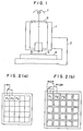
- FIG. 1 is a view used to explain the construction of the prior art device.
- a lens barrel 1 is securely mounted on a stand 2 and a main table 4 upon which is mounted a mask 3 is disposed below the stand 2.
- An original 5 is disposed at the upper end of the lens barrel 1 while a projection lens 6 is mounted at the lower end thereof.
- a light source 7 which is disposed upwardly of the original 5
- the pattern or image on the original 5 is focused through the projection lens 6 over the mask 3.
- Fig. 2 shows a top view of a mask prepared by the device as shown in Fig. 1.
- the original 5 is magnified by five or ten times (this magnification ratio is fixed) and is, in turn, reduced through the projection lens 6 to 1/5 or 1/10 (the reduction ratio is also fixed).
- the reduced image is focused upon a predetermined portion (for instance at P 1 in Fig. 2(a)) of the mask 3. Every time when the image is focused, the main table 4 is stepped .(by a distance a in Fig. 2(a)), whereby patterns are successively transferred. (For instance, the patterns are transferred in the order of P 1 , P 2 , P 3 and so on in Fig. 2(a)).
- the process for manufacture of semiconductor devices includes a heat treatment step so that thermal deformations and shrinkage of wafers result.
- the position and size of a pattern transferred on a wafer are deviated from a desired position and a desired size.
- this "deviation" is very small so that the size of one pattern; that is, the pattern transfer reduction is not changed, but the positions where the patterns are focused; that is, the step is varied in response to the enlargement or reduction of the wafer.
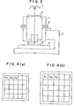
- Fig. 3 is a view used to explain the construction of the first embodiment and same reference numerals are used to designate similar parts throughout the figures.
- a control mechanism 8 is interposed between the upper and lower halves of the lens barrel 1 so that the length of-the lens barrel 1 can be varied and consequently the reduction can be finely adjusted.
- the length of the lens barrel remains unchanged because if the length is varied, the characteristics of the high resolving power lens are adversely affected, but according to the experiments conducted by the inventors it is confirmed that no adverse effect will occur even when the length of the lens barrel is varied by 0.1%.
- the control mechanism 8 may-be a piezoelectric element which changes its thickness when applied with a voltage or a motor and cam mechanism. By changing the length of the lens barrel, the size of a pattern focused on the mask 3 mounted on the main table 4 is varied or adjusted.
- Fig. 4 shows a top view of a mask prepared by the device as shown in Fig. 3.
- the patterns are transferred on the mask 3 as shown in Fig. 4(a).
- the mask 3 is subjected to a heat treatment, it is deformed.
- the rate of shrinkage due to heat treatment is previously obtained so that in response to the rate of shrinkage the rate of reduction is varied by increasing or decreasing the length of the lens barrel 1 by the control mechanism 8.
- the main table 4 and hence the mask 3 are successively stepped as indicated by P 1 , P 2' P 3 and so on. Therefore, the patterns whose "deviations" are minimized can be obtained as shown in Fig. 4(b).
- the position of the projection lens or the original may be varied.
- a zoom lens may be used as a projection lens.
- a second embodiment of a pattern transfer device in accordance with the present invention is shown in Fig. 5.
- a lens barrel 1 is mounted on a stand 2 and a main table 4 upon which is mounted a semiconductor wafer 3 is disposed below the stand 2.
- An original 5 is mounted at the lens barrel 1 while the projection lens 6 is mounted at the lower end of the lens barrel 1.
- a light source 7 is disposed upwardly of the original 5 and a movable mirror 11 is interposed between the original 5 and the light source 7 so that the pattern on the semiconductor wafer 3 may be directed toward a pattern position detector 10.
- a laser interferometer 9 is mounted on the main table 4 so that the position may be detected.
- the control mechanism 8 for making the fine adjustment of the rate of reduction is interposed between the upper and lower halves of the lens barrel 1 so that the length of the lens barrel 1 can be varied.
- the control mechanism 8 may be a piezoelectric element or a motor and cam link as described before.
- the mode of operation will be described.
- the movable mirror 11 is moved out of the optical path from the light source 7 to the original 5 and a pattern P is transferred. That is, the light is projected from the light source 7 to the original 5 so that a reduced pattern is focused on the semiconductor wafer 3 through the projection lens 6.
- the main table 4 is stepped by a distance A and another pattern P is transferred on the semiconductor wafer 3.
- the semiconductor wafer 3 is subjected to a heat treatment step, it is expanded so that a pattern P is enlarged as indicated at (b) in Fig. 6. As a result, the step is increased from A to A + AA. Thereafter a reduced pattern Q is superimposed on the pattern P.
- the movable mirror 11 is moved to the position shown in Fig. 5 so that the pattern transferred on the semiconductor wafer 3 is received or detected by the pattern position detector 10.
- the pattern position detector 10 detects the alignment mark a of the pattern P so that the expanded step A + AA can be detected.
- An extremely small "deviation" AA can be detected by the high precision laser interferometer 9 mounted on the main table 4.
- the transfer reduction of a pattern Q is computed by a control system (not shown).
- the reduction ratio N A + AA of the pattern Q can be obtained from the following equation: where N A is the reduction ratio when the step is A.
- the control mechanism 8 is so operated that the length of the lens barrel 1 is varied and consequently the transfer reduction ratio becomes N A + ⁇ A.
- the movable mirror 11 is moved out of the optical path from the light source 7 to the original 5 and the pattern Q is transferred at the reduction ratio of N A + AA.
- the next pattern Q is transferred in a manner substantially similar to that described above. That is, the step is detected from the alignment marks a of the pattern P and in response to the detected step, the reduction ratio is corrected and then the pattern Q is transferred. In like manner, the patterns Q are successively transferred as shown in Fig. 6(c).
- the patterns may be transferred by minimum misalignment or misregistration.
- the reduction ratio' is varied so that the correct alignment between the patterns P and Q can be ensured even when the semiconductor wafer is locally deformed.
- the transfer reduction ratio is varied every time when a pattern is transferred, but it is to be understood that the steps between typical points on the semiconductor wafer are measured and the average step is obtained so that the reduction ratio can be determined in response .to the average step.
- a pattern may be transferred not only on the surface of a semiconductor wafer but also on a semiconductor mask or the like.
- a prior art device and method for transferring patterns over the surface of a photomask or a semiconductor wafer by the step-and-repeat procedure and by reducing the original pattern is provided with a reduction control means for making the fine adjustment of the reduction so that the size of each pattern can be corrected. Therefore even when a wafer is deformed or shrinked due to heat treatment, not only the step can be corrected but also the size of a pattern can be adjusted so that the misalignment between the patterns can be reduced to a minimum. For instance, if a pattern consisting of 10 xlO elements (patterns) is enlarged by 1. micrometer per 100 millimeter, each element (pattern) is corrected by 0.1 micrometer per 10 millimeter. Then, the most influential cause of the primary misalignment between the patterns can be removed.
- each pattern transfer device has its own temperature so that.it has been considered that it is impossible to transfer patterns on a wafer or the like without any misalignment or misregistration with different pattern transfer devices.
- patterns can be transferred without any misalignment or misregistration with a plurality of pattern transfer devices.
Landscapes
- Physics & Mathematics (AREA)
- General Physics & Mathematics (AREA)
- Exposure And Positioning Against Photoresist Photosensitive Materials (AREA)
- Exposure Of Semiconductors, Excluding Electron Or Ion Beam Exposure (AREA)
- Projection-Type Copiers In General (AREA)
Applications Claiming Priority (2)
| Application Number | Priority Date | Filing Date | Title |
|---|---|---|---|
| JP58022511A JPS59150424A (ja) | 1983-02-14 | 1983-02-14 | 半導体装置の製造装置および方法 |
| JP22511/83 | 1983-02-14 |
Publications (3)
| Publication Number | Publication Date |
|---|---|
| EP0116940A2 true EP0116940A2 (fr) | 1984-08-29 |
| EP0116940A3 EP0116940A3 (en) | 1985-01-30 |
| EP0116940B1 EP0116940B1 (fr) | 1988-04-20 |
Family
ID=12084781
Family Applications (1)
| Application Number | Title | Priority Date | Filing Date |
|---|---|---|---|
| EP84101498A Expired EP0116940B1 (fr) | 1983-02-14 | 1984-02-14 | Dispositif de transfert de motifs ainsi que son procédé |
Country Status (4)
| Country | Link |
|---|---|
| US (1) | US4577945A (fr) |
| EP (1) | EP0116940B1 (fr) |
| JP (1) | JPS59150424A (fr) |
| DE (1) | DE3470611D1 (fr) |
Cited By (2)
| Publication number | Priority date | Publication date | Assignee | Title |
|---|---|---|---|---|
| US4737823A (en) * | 1986-06-16 | 1988-04-12 | U.S. Philips Corporation | Opto-lithographic device comprising a displaceable lens system and method of controlling the imaging properties of lens system in such a device |
| EP0531102A1 (fr) * | 1991-09-04 | 1993-03-10 | Canon Kabushiki Kaisha | Appareil de réproduction avec dispositif d'alignement et méthode d'exposition pour la fabrication d'un dispositif semi-conducteur |
Families Citing this family (4)
| Publication number | Priority date | Publication date | Assignee | Title |
|---|---|---|---|---|
| JPH0722101B2 (ja) * | 1985-08-29 | 1995-03-08 | 株式会社ニコン | 投影型露光装置用遮風装置 |
| ATE63008T1 (de) * | 1986-09-05 | 1991-05-15 | Staude Foto Chemie Eva | Vorrichtung und verfahren zur verfilmung von dokumenten. |
| JPS63164212A (ja) * | 1986-12-26 | 1988-07-07 | Hitachi Ltd | 縮小投影露光装置 |
| JP5134767B2 (ja) * | 2005-04-19 | 2013-01-30 | 株式会社オーク製作所 | 描画データ補正機能を有する描画装置 |
Family Cites Families (8)
| Publication number | Priority date | Publication date | Assignee | Title |
|---|---|---|---|---|
| US3744902A (en) * | 1968-10-23 | 1973-07-10 | Siemens Ag | Device for producing a photo-varnish mask |
| US4108941A (en) * | 1976-04-26 | 1978-08-22 | Dolco Packaging Corporation | Shear molding of reinforced latch |
| FR2388300A1 (fr) * | 1977-04-20 | 1978-11-17 | Thomson Csf | Dispositif optique de projection de motifs comportant un asservissement de focalisation a grandissement constant |
| US4190325A (en) * | 1977-12-02 | 1980-02-26 | Ford Motor Company | Thermal compensator assembly |
| US4383757A (en) * | 1979-04-02 | 1983-05-17 | Optimetrix Corporation | Optical focusing system |
| DE3070825D1 (en) * | 1979-04-02 | 1985-08-08 | Eaton Optimetrix Inc | A system for positioning a utilization device |
| US4414749A (en) * | 1979-07-02 | 1983-11-15 | Optimetrix Corporation | Alignment and exposure system with an indicium of an axis of motion of the system |
| JPS57192929A (en) * | 1981-05-25 | 1982-11-27 | Hitachi Ltd | Projector provided with automatic focusing function |
-
1983
- 1983-02-14 JP JP58022511A patent/JPS59150424A/ja active Pending
-
1984
- 1984-02-10 US US06/578,815 patent/US4577945A/en not_active Expired - Lifetime
- 1984-02-14 DE DE8484101498T patent/DE3470611D1/de not_active Expired
- 1984-02-14 EP EP84101498A patent/EP0116940B1/fr not_active Expired
Cited By (3)
| Publication number | Priority date | Publication date | Assignee | Title |
|---|---|---|---|---|
| US4737823A (en) * | 1986-06-16 | 1988-04-12 | U.S. Philips Corporation | Opto-lithographic device comprising a displaceable lens system and method of controlling the imaging properties of lens system in such a device |
| EP0531102A1 (fr) * | 1991-09-04 | 1993-03-10 | Canon Kabushiki Kaisha | Appareil de réproduction avec dispositif d'alignement et méthode d'exposition pour la fabrication d'un dispositif semi-conducteur |
| US5270771A (en) * | 1991-09-04 | 1993-12-14 | Canon Kabushiki Kaisha | Aligner and exposure method for manufacturing semiconductor device |
Also Published As
| Publication number | Publication date |
|---|---|
| JPS59150424A (ja) | 1984-08-28 |
| EP0116940B1 (fr) | 1988-04-20 |
| DE3470611D1 (en) | 1988-05-26 |
| EP0116940A3 (en) | 1985-01-30 |
| US4577945A (en) | 1986-03-25 |
Similar Documents
| Publication | Publication Date | Title |
|---|---|---|
| US4811055A (en) | Projection exposure apparatus | |
| US4734746A (en) | Exposure method and system for photolithography | |
| EP0480616B1 (fr) | Appareil d'exposition par projection avec un dispositif pour compenser l'aberration d'une lentille de projection | |
| US4708466A (en) | Exposure apparatus | |
| US6014455A (en) | Projection exposure apparatus and device manufacturing method | |
| US4488806A (en) | Shot arranging method in a divisional printing apparatus | |
| EP0116940B1 (fr) | Dispositif de transfert de motifs ainsi que son procédé | |
| US6847432B2 (en) | Alignment system and projection exposure apparatus | |
| JP2914315B2 (ja) | 走査型縮小投影露光装置及びディストーション測定方法 | |
| EP0230648A2 (fr) | Procédé de formation de marques d'alignement dans un corps semi-conducteur | |
| JP2000195784A (ja) | 露光装置およびデバイス製造方法 | |
| US5311282A (en) | High precision stepping aligner having a spiral stepping pattern | |
| US6256085B1 (en) | Exposure apparatus | |
| JPS60138926A (ja) | パタ−ン転写装置 | |
| JP3068785B2 (ja) | 投影露光装置、または投影露光方法、及びその投影露光方法を用いたデバイス製造方法、及びそのデバイス製造方法により製造されたデバイス | |
| JP3550034B2 (ja) | 露光方法及び露光装置 | |
| JPH0550849B2 (fr) | ||
| JPH1174190A (ja) | X線露光装置 | |
| JP2876406B2 (ja) | 露光装置及び露光方法 | |
| KR100390818B1 (ko) | 반도체균일패턴형성방법 | |
| US20070072128A1 (en) | Method of manufacturing an integrated circuit to obtain uniform exposure in a photolithographic process | |
| JPS6097359A (ja) | 投影形露光装置 | |
| KR0144412B1 (ko) | 노광장치의 렌즈 축소율 조정방법 | |
| JP2001160533A (ja) | 投影露光装置およびデバイス製造方法 | |
| JP2005109333A (ja) | 半導体製造装置およびデバイス製造方法 |
Legal Events
| Date | Code | Title | Description |
|---|---|---|---|
| PUAI | Public reference made under article 153(3) epc to a published international application that has entered the european phase |
Free format text: ORIGINAL CODE: 0009012 |
|
| 17P | Request for examination filed |
Effective date: 19840214 |
|
| AK | Designated contracting states |
Designated state(s): DE FR GB IT |
|
| PUAL | Search report despatched |
Free format text: ORIGINAL CODE: 0009013 |
|
| AK | Designated contracting states |
Designated state(s): DE FR GB IT |
|
| 17Q | First examination report despatched |
Effective date: 19860610 |
|
| GRAA | (expected) grant |
Free format text: ORIGINAL CODE: 0009210 |
|
| AK | Designated contracting states |
Kind code of ref document: B1 Designated state(s): DE FR GB IT |
|
| REF | Corresponds to: |
Ref document number: 3470611 Country of ref document: DE Date of ref document: 19880526 |
|
| ET | Fr: translation filed | ||
| ITF | It: translation for a ep patent filed | ||
| PLBE | No opposition filed within time limit |
Free format text: ORIGINAL CODE: 0009261 |
|
| STAA | Information on the status of an ep patent application or granted ep patent |
Free format text: STATUS: NO OPPOSITION FILED WITHIN TIME LIMIT |
|
| 26N | No opposition filed | ||
| ITTA | It: last paid annual fee | ||
| PGFP | Annual fee paid to national office [announced via postgrant information from national office to epo] |
Ref country code: GB Payment date: 19970205 Year of fee payment: 14 |
|
| PGFP | Annual fee paid to national office [announced via postgrant information from national office to epo] |
Ref country code: FR Payment date: 19970211 Year of fee payment: 14 |
|
| PGFP | Annual fee paid to national office [announced via postgrant information from national office to epo] |
Ref country code: DE Payment date: 19970221 Year of fee payment: 14 |
|
| PG25 | Lapsed in a contracting state [announced via postgrant information from national office to epo] |
Ref country code: GB Free format text: LAPSE BECAUSE OF NON-PAYMENT OF DUE FEES Effective date: 19980214 |
|
| PG25 | Lapsed in a contracting state [announced via postgrant information from national office to epo] |
Ref country code: FR Free format text: THE PATENT HAS BEEN ANNULLED BY A DECISION OF A NATIONAL AUTHORITY Effective date: 19980228 |
|
| GBPC | Gb: european patent ceased through non-payment of renewal fee |
Effective date: 19980214 |
|
| PG25 | Lapsed in a contracting state [announced via postgrant information from national office to epo] |
Ref country code: DE Free format text: LAPSE BECAUSE OF NON-PAYMENT OF DUE FEES Effective date: 19981103 |
|
| REG | Reference to a national code |
Ref country code: FR Ref legal event code: ST |