EP0116972A2 - Transcodeur commutable - Google Patents
Transcodeur commutable Download PDFInfo
- Publication number
- EP0116972A2 EP0116972A2 EP84101682A EP84101682A EP0116972A2 EP 0116972 A2 EP0116972 A2 EP 0116972A2 EP 84101682 A EP84101682 A EP 84101682A EP 84101682 A EP84101682 A EP 84101682A EP 0116972 A2 EP0116972 A2 EP 0116972A2
- Authority
- EP
- European Patent Office
- Prior art keywords
- input
- output
- switch
- stage
- differential amplifier
- Prior art date
- Legal status (The legal status is an assumption and is not a legal conclusion. Google has not performed a legal analysis and makes no representation as to the accuracy of the status listed.)
- Granted
Links
Images
Classifications
-
- H—ELECTRICITY
- H03—ELECTRONIC CIRCUITRY
- H03M—CODING; DECODING; CODE CONVERSION IN GENERAL
- H03M5/00—Conversion of the form of the representation of individual digits
- H03M5/02—Conversion to or from representation by pulses
- H03M5/04—Conversion to or from representation by pulses the pulses having two levels
- H03M5/06—Code representation, e.g. transition, for a given bit cell depending only on the information in that bit cell
- H03M5/12—Biphase level code, e.g. split phase code, Manchester code; Biphase space or mark code, e.g. double frequency code
-
- H—ELECTRICITY
- H03—ELECTRONIC CIRCUITRY
- H03M—CODING; DECODING; CODE CONVERSION IN GENERAL
- H03M5/00—Conversion of the form of the representation of individual digits
- H03M5/02—Conversion to or from representation by pulses
- H03M5/16—Conversion to or from representation by pulses the pulses having three levels
- H03M5/18—Conversion to or from representation by pulses the pulses having three levels two levels being symmetrical with respect to the third level, i.e. balanced bipolar ternary code
Definitions
- the invention relates to a switchable transcoder for AMI-coded signals into signals in binary code or in differential binary code.
- the AMI code which is a redundant bipolar code, is often used to transmit digital signals over copper lines.
- the regeneration of AMI-coded signals on the link can be carried out in such a way that the AMI-coded signals are divided into a positive and a negative pulse train and both pulse trains are regenerated as unipolar signals.
- a less complex method of regenerating AMI-coded signals is to transcode them into the so-called differential binary code, so that only a binary signal then has to be regenerated.
- the transcoding can take place, for example, in that the received AMI-coded signals are supplied to a Schmitt trigger after the equalization, the switching thresholds of the Schmitt trigger corresponding to the threshold voltages of the AMI-coded signal.
- a transcoder is desired at the digital interfaces, which converts AMI-coded signals either into the differential binary code or into the binary code.
- the object of the invention is therefore to provide a simple and easily integrable transcoder which can be switched between the transcoding from the AMI code to the binary code and from the AMI code to the differential binary code.
- a differential amplifier arrangement which contains two emitter-coupled differential amplifiers, each with an input stage and a reference stage, that the stage inputs of the two input stages are connected to one another and to a signal input, in that the stage inputs of the reference stages are each separately connected to a reference voltage source are connected and the voltage of the first reference voltage source corresponds to the threshold voltage of the negative input pulses and the voltage of the second reference voltage source corresponds to the threshold voltage of the positive input pulses, that the output terminal of the input stage of the emitter-coupled differential amplifier is connected to the output terminal of the reference stage of the second and the output terminal of the reference stage of the first emitter-coupled Differential amplifier are connected to the output terminal of the input stage of the second emitter-coupled differential amplifier that with one of the two pairs of output connections and thus with the output connection of the differential amplifier arrangement via a switch a clocked D flip-flop is connected, the non-inverting output of which is connected to the output connection of the transcoder
- the transcoder according to the invention offers the considerable advantage that it can be used up to step speeds of approximately 750 Mbit / s using commercially available components.
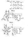
- a digital signal is shown in FIG. 1; that is in the top line in the AMI code, in the middle line in the binary code and in the bottom line in the difference binary code.
- a digital signal is shown in FIG. 1; that is in the top line in the AMI code, in the middle line in the binary code and in the bottom line in the difference binary code.
- one pulses of alternating polarity always follow one another in the upper line. These lead to one impulses in the Binary code corresponding to the middle line and for a change of the logic level in the signal of the lower line according to the difference binary code (DBC).
- DBC difference binary code
- the switchable transcoder according to FIG. 2 contains in the signal flow one after the other a differential amplifier arrangement, a level adjustment stage PA, a switch S and a D flip-flop DFF.
- the differential amplifier arrangement contains two emitter-coupled differential amplifiers which contain the first and the second transistor T1, T2 and the third and the fourth transistor T3, T4.
- the first and the fourth transistor T1, T4 each form the input stage and the second and the third transistor T2, T3 form the reference stage of the respective differential amplifier.
- the base connections of the first and the fourth transistor T1, T4 are connected to one another and to an input connection E, next to which the AMI-coded input signal is shown with a positive and a negative input pulse.
- the emitter connection of the first transistor T1 is connected via a first current source I1 with operating voltage -Ub and directly to the emitter connection of the second transistor T2.
- the emitter connection of the fourth transistor T4 is connected via a second current source I2 to the operating voltage connection -Ub and also directly to the emitter connection of the third transistor T3.
- the base connection of the second transistor T2 is connected to a source U1 for a first reference voltage and the base connection of the third transistor T3 is connected to a second source U2 for a further reference voltage.
- the voltages of the first and second reference voltage sources are at the threshold value, i.e. half the pulse amplitude of the positive and negative input pulses, while the base connections of the first and fourth transistors T1, T4 receive a voltage U3 corresponding to the logic zero level of the input signals.
- the collector terminal of the first transistor T1 is connected to the collector terminal of the third transistor T3, via a second resistor R2 with reference potential and also to an output terminal Y.
- the collector terminal of the second transistor T2 is connected to the collector terminal of the fourth transistor T4, to an output terminal 7 for an inverse output signal and also to a reference potential via a first resistor R1.
- the input of a stage PA for level adjustment is connected to one of the two output connections Y, Y; the assignment of the respective output connection depends on whether or not a phase shift of the transmitted signal by 180 degrees takes place in the level adjustment stage PA and whether an inverting or a non-inverting input is available for the downstream D flip-flop.
- the second and third signal inputs of a switch S are connected to the output of the stage PA for level adjustment.
- the fourth signal input of the switch S is connected to a source HP for the logic single level, the first signal output 5 of the switch S is connected to the D input of the D flip-flop and the second signal output 6 of the switch S is connected to the clock takeover input CE (clock enable ) connected to the D flip-flop.
- the clock input C1 of the D flip-flop is connected to a source Ts for a clock signal with a repetition frequency corresponding to the bit rate of the binary signals to be generated, while the output A of the recoder is connected to the non-inverting output Q of the D flip-flop.
- the first and fourth transistors T1, T4 conduct while the second and third transistors T2, T3 are blocked.
- the second and third transistors T2, T3 conduct, while the first and fourth transistors T1, T4 are blocked.
- the collector current of a transistor therefore flows through the first and second resistors R1, R2 in the case of both positive and negative input pulses. This collector current generates a more negative potential at the first resistor R1 and thus at the inverting output Y than at the zero state at the input E and at the second resistor R2, that is to say at the non-inverting output Y, a more positive potential, to which the logic one state has been assigned.
- the level PA input signal for level adjustment is therefore in the logic one state with both positive and negative AMI input pulses.
- the switch connected to the output of stage PA for level adjustment connects the first signal input 1 to the first signal output 5 and the third signal input 3 to the second signal output 6; In this switch position, output signals are generated in the differential binary code.
- the switch S is in the second switch position and then connects the second signal input 2 to the first signal output 5 and the fourth signal input 4 to the second signal output 6.
- the switching of the flip-flop is additionally controlled by the output signal of the differential amplifier arrangement. If the clock take-over input CE is at the logic zero level, then the clock input of the D flip-flop is blocked. Only in the event that the logic single level is present at the non-inverting output Y of the differential amplifier arrangement does the D flip-flop switch to the opposite output state, provided that the stage PA for level adjustment does not phase change.
- FIG. 3 shows a practical exemplary embodiment of the recoder according to FIG. 2.
- a base voltage divider consisting of the resistors R3 and R4 was provided, which is connected on one side to reference potential and on the other side to operating voltage -Ub,
- a coupling capacitor C was provided, which is used for the DC separation of the input E from the base connections.
- the base bias generated corresponds to the zero level of the AMI-coded input signals.
- a master-slave D flip-flop was used, which has an inverse clock input CE contains.
- the base connection of the fifth transistor T5 connected as an emitter follower stage was connected to the inverse output connection 7 of the differential amplifier arrangement.
- the output of the emitter follower is connected to the second and third signal inputs 2, 3 of the switch S, while the first signal input 1 of this switch is connected to the inverting output Q of the D flip-flop and the fourth signal input 4 is at zero level, so that it is in was not further connected in the present case.
- the output connection A of the recoder is with the inverting output Q connected to the D flip-flop.
- the master-slave D flip-flop DFF2 therefore switches over when the inverse clock transfer input is present CE the zero level lies, while the clock input is blocked when the level is applied.
- the inverting output Q was the inversion of the signal at the D input of the D flip-flop by connecting it to the inverting output Y the differential amplifier arrangement compensated.
- logic gates can also be introduced into the signal path for signal switching in a known manner, which in turn would be controlled by mechanical switches. This can reduce signal distortion at high walking speeds.
Landscapes
- Engineering & Computer Science (AREA)
- Theoretical Computer Science (AREA)
- Dc Digital Transmission (AREA)
- Supplying Of Containers To The Packaging Station (AREA)
- Transmitters (AREA)
- Electrophonic Musical Instruments (AREA)
- Manipulation Of Pulses (AREA)
Priority Applications (1)
| Application Number | Priority Date | Filing Date | Title |
|---|---|---|---|
| AT84101682T ATE43763T1 (de) | 1983-02-22 | 1984-02-17 | Umschaltbarer umcodierer. |
Applications Claiming Priority (2)
| Application Number | Priority Date | Filing Date | Title |
|---|---|---|---|
| DE3306113A DE3306113A1 (de) | 1983-02-22 | 1983-02-22 | Umschaltbarer umcodierer |
| DE3306113 | 1983-02-22 |
Publications (3)
| Publication Number | Publication Date |
|---|---|
| EP0116972A2 true EP0116972A2 (fr) | 1984-08-29 |
| EP0116972A3 EP0116972A3 (en) | 1987-04-22 |
| EP0116972B1 EP0116972B1 (fr) | 1989-05-31 |
Family
ID=6191505
Family Applications (1)
| Application Number | Title | Priority Date | Filing Date |
|---|---|---|---|
| EP84101682A Expired EP0116972B1 (fr) | 1983-02-22 | 1984-02-17 | Transcodeur commutable |
Country Status (3)
| Country | Link |
|---|---|
| EP (1) | EP0116972B1 (fr) |
| AT (1) | ATE43763T1 (fr) |
| DE (2) | DE3306113A1 (fr) |
Family Cites Families (1)
| Publication number | Priority date | Publication date | Assignee | Title |
|---|---|---|---|---|
| US3434059A (en) * | 1966-09-06 | 1969-03-18 | Us Army | Bipolar to two-level binary code translator |
-
1983
- 1983-02-22 DE DE3306113A patent/DE3306113A1/de not_active Withdrawn
-
1984
- 1984-02-17 AT AT84101682T patent/ATE43763T1/de not_active IP Right Cessation
- 1984-02-17 DE DE8484101682T patent/DE3478553D1/de not_active Expired
- 1984-02-17 EP EP84101682A patent/EP0116972B1/fr not_active Expired
Also Published As
| Publication number | Publication date |
|---|---|
| DE3478553D1 (en) | 1989-07-06 |
| ATE43763T1 (de) | 1989-06-15 |
| EP0116972A3 (en) | 1987-04-22 |
| EP0116972B1 (fr) | 1989-05-31 |
| DE3306113A1 (de) | 1984-08-23 |
Similar Documents
| Publication | Publication Date | Title |
|---|---|---|
| DE3442613C2 (fr) | ||
| EP0111309B1 (fr) | Décodeur CMI | |
| DE3030172A1 (de) | Regenerator fuer mehrstufige digitale signale | |
| EP0094624A2 (fr) | Dispositif pour la génération de signaux quaternaires | |
| EP0116972B1 (fr) | Transcodeur commutable | |
| EP0073400A1 (fr) | Régénérateur pour signaux digitaux à réaction quantifiée | |
| DE2850129A1 (de) | Schaltungsanordnung zur umwandlung von binaeren digitalsignalen in pseudoternaere wechselimpulse | |
| DE3010535C2 (de) | Regenerator für digitale Signale | |
| DE1181273B (de) | Resttraeger-Steuerung bei Einseitenband-UEbertragung | |
| DE3023833C2 (de) | Regenerator für quaternäre PCM-Signale | |
| DE69902205T2 (de) | Schaltung zur Wiedergewinnung der Gleichstromkomponente | |
| EP0292817A2 (fr) | Circuit pour l'obtention de signaux numériques bipolaires | |
| EP0042621B1 (fr) | Régénérateur pour signaux numériques multiniveaux | |
| DE2900599C2 (de) | Verfahren und Anordnung zur Regenerierung des zur Übertragung verwendeten Hauptenergiebereichs eines trägerfrequenten digitalen Signals | |
| DE2833267B1 (de) | Verfahren und Anordnung zur Regenerierung eines n-stufigen digitalen Signals | |
| DE4228010C2 (de) | Leitungsempfänger | |
| EP0119600A2 (fr) | Régénération de signaux numériques ayant une vitesse de bit élevée | |
| DE3030115C2 (de) | Differenzverstärkeranordnung als Schwellenwertschalter für digitale Signale | |
| DE2407954C2 (de) | PCM-Regenerator | |
| DE3043372A1 (de) | Regenerator fuer n-stufige digitale signale | |
| DE3119485A1 (de) | Regenerator fuer digitale signale | |
| DE1537251C3 (de) | Nach dem Master-Slave-Prinzip arbeitender bistabiler Einphasenverzögerungsmultlvibrator | |
| EP0399153A1 (fr) | Régénérateur pour signaux numériques | |
| DE3224479A1 (de) | Anordnung zur erzeugung gleichstromfeier pseudoternaerer signale | |
| DE3248624A1 (de) | Schaltungsanordnung zur erzeugung eines digitalen binaeren datensignals und eines zugehoerigen taktsignals aus einem cmi-codierten signals, dessen taktfrequenz ueber 30 mhz liegt |
Legal Events
| Date | Code | Title | Description |
|---|---|---|---|
| PUAI | Public reference made under article 153(3) epc to a published international application that has entered the european phase |
Free format text: ORIGINAL CODE: 0009012 |
|
| AK | Designated contracting states |
Designated state(s): AT BE CH DE FR GB IT LI NL |
|
| 17P | Request for examination filed |
Effective date: 19841221 |
|
| PUAL | Search report despatched |
Free format text: ORIGINAL CODE: 0009013 |
|
| AK | Designated contracting states |
Kind code of ref document: A3 Designated state(s): AT BE CH DE FR GB IT LI NL |
|
| 17Q | First examination report despatched |
Effective date: 19881115 |
|
| GRAA | (expected) grant |
Free format text: ORIGINAL CODE: 0009210 |
|
| AK | Designated contracting states |
Kind code of ref document: B1 Designated state(s): AT BE CH DE FR GB IT LI NL |
|
| PG25 | Lapsed in a contracting state [announced via postgrant information from national office to epo] |
Ref country code: NL Effective date: 19890531 Ref country code: IT Free format text: LAPSE BECAUSE OF FAILURE TO SUBMIT A TRANSLATION OF THE DESCRIPTION OR TO PAY THE FEE WITHIN THE PRESCRIBED TIME-LIMIT;WARNING: LAPSES OF ITALIAN PATENTS WITH EFFECTIVE DATE BEFORE 2007 MAY HAVE OCCURRED AT ANY TIME BEFORE 2007. THE CORRECT EFFECTIVE DATE MAY BE DIFFERENT FROM THE ONE RECORDED. Effective date: 19890531 Ref country code: GB Effective date: 19890531 Ref country code: FR Free format text: THE PATENT HAS BEEN ANNULLED BY A DECISION OF A NATIONAL AUTHORITY Effective date: 19890531 Ref country code: BE Effective date: 19890531 |
|
| REF | Corresponds to: |
Ref document number: 43763 Country of ref document: AT Date of ref document: 19890615 Kind code of ref document: T |
|
| REF | Corresponds to: |
Ref document number: 3478553 Country of ref document: DE Date of ref document: 19890706 |
|
| EN | Fr: translation not filed | ||
| NLV1 | Nl: lapsed or annulled due to failure to fulfill the requirements of art. 29p and 29m of the patents act | ||
| GBV | Gb: ep patent (uk) treated as always having been void in accordance with gb section 77(7)/1977 [no translation filed] | ||
| PG25 | Lapsed in a contracting state [announced via postgrant information from national office to epo] |
Ref country code: AT Effective date: 19900217 |
|
| PG25 | Lapsed in a contracting state [announced via postgrant information from national office to epo] |
Ref country code: LI Effective date: 19900228 Ref country code: CH Effective date: 19900228 |
|
| PLBE | No opposition filed within time limit |
Free format text: ORIGINAL CODE: 0009261 |
|
| STAA | Information on the status of an ep patent application or granted ep patent |
Free format text: STATUS: NO OPPOSITION FILED WITHIN TIME LIMIT |
|
| 26N | No opposition filed | ||
| REG | Reference to a national code |
Ref country code: CH Ref legal event code: PL |
|
| PGFP | Annual fee paid to national office [announced via postgrant information from national office to epo] |
Ref country code: DE Payment date: 19940419 Year of fee payment: 11 |
|
| PG25 | Lapsed in a contracting state [announced via postgrant information from national office to epo] |
Ref country code: DE Effective date: 19951101 |