EP0117007A2 - Convertisseur analogique-numérique utilisant la conversion de valeur absolue - Google Patents
Convertisseur analogique-numérique utilisant la conversion de valeur absolue Download PDFInfo
- Publication number
- EP0117007A2 EP0117007A2 EP84200218A EP84200218A EP0117007A2 EP 0117007 A2 EP0117007 A2 EP 0117007A2 EP 84200218 A EP84200218 A EP 84200218A EP 84200218 A EP84200218 A EP 84200218A EP 0117007 A2 EP0117007 A2 EP 0117007A2
- Authority
- EP
- European Patent Office
- Prior art keywords
- amplifier
- signal
- gain
- amplifiers
- absolute
- Prior art date
- Legal status (The legal status is an assumption and is not a legal conclusion. Google has not performed a legal analysis and makes no representation as to the accuracy of the status listed.)
- Withdrawn
Links
- 238000006243 chemical reaction Methods 0.000 title description 7
- 230000000295 complement effect Effects 0.000 claims description 9
- 230000004044 response Effects 0.000 claims description 7
- 230000001105 regulatory effect Effects 0.000 abstract description 2
- 239000000872 buffer Substances 0.000 description 17
- 239000004065 semiconductor Substances 0.000 description 7
- 238000010586 diagram Methods 0.000 description 6
- 230000008859 change Effects 0.000 description 5
- 239000002131 composite material Substances 0.000 description 5
- 230000006870 function Effects 0.000 description 5
- 238000013459 approach Methods 0.000 description 4
- 238000006880 cross-coupling reaction Methods 0.000 description 4
- 230000007423 decrease Effects 0.000 description 4
- 238000000034 method Methods 0.000 description 4
- 238000004519 manufacturing process Methods 0.000 description 3
- 238000012546 transfer Methods 0.000 description 3
- 238000013461 design Methods 0.000 description 2
- 230000003321 amplification Effects 0.000 description 1
- 230000008901 benefit Effects 0.000 description 1
- 230000033228 biological regulation Effects 0.000 description 1
- 238000013500 data storage Methods 0.000 description 1
- 230000003247 decreasing effect Effects 0.000 description 1
- 238000002955 isolation Methods 0.000 description 1
- 229910044991 metal oxide Inorganic materials 0.000 description 1
- 150000004706 metal oxides Chemical class 0.000 description 1
- 238000012986 modification Methods 0.000 description 1
- 230000004048 modification Effects 0.000 description 1
- 238000003199 nucleic acid amplification method Methods 0.000 description 1
- 238000012545 processing Methods 0.000 description 1
- 238000005070 sampling Methods 0.000 description 1
- 238000012360 testing method Methods 0.000 description 1
Images



Classifications
-
- H—ELECTRICITY
- H03—ELECTRONIC CIRCUITRY
- H03M—CODING; DECODING; CODE CONVERSION IN GENERAL
- H03M1/00—Analogue/digital conversion; Digital/analogue conversion
- H03M1/12—Analogue/digital converters
- H03M1/34—Analogue value compared with reference values
- H03M1/38—Analogue value compared with reference values sequentially only, e.g. successive approximation type
- H03M1/44—Sequential comparisons in series-connected stages with change in value of analogue signal
Definitions
- This invention relates generally to analog-to-digital (A/D) converters suitable for semiconductor integrated circuits and particularly to such A/D converters employing absolute-value conversion techniques.
- FIG. 1 it illustrates a conventional absolute-value converter in which an analog voltage signal V I is converted into an N-bit digital signal represented as bits 1, 2, ...J, ... N-1, and N.
- Bit 1 is the most significant bit (MSB), while bit N is the least significant bit (LSB).
- an input circuit 10 operates on analog voltage V I to produce an analog input signal V I1 which is supplied to the first amplifier A 1 in a chain of N-1 main absolute-value differential amplifiers A 1 , A 2 , ...A J '... and A N-1 .
- each amplifier A J amplifies the absolute value of their voltage difference to produce an output signal V OJ which is supplied as the mainline input V IJ+1 to the next amplifier A J+1
- This procedure is followed with all of outputs V OJ except output V ON-1 which is supplied as mainline input V IN to a buffer 12 that receives a reference input but may not be an absolute-value differential amplifier.
- a set of N comparators C 1 , ... C J' ... C N-1' and C N corresponding respectively to amplifiers A 1 ,... A J , ...and A N-1 and buffer generates the digital signal.
- each comparator C J generates bit J using the inputs to corresponding amplifier A J or buffer 12.
- comparator C J does not directly compare these inputs but instead compares a pair of intermediate signals V YJ and V ZJ generated from the inputs.
- the generation of signals V YJ and V ZJ is represented by the dashed lines within each amplifier A J or buffer 12.
- each amplifier A J has an optimum gain of precisely 2.
- Mainline inputs V I1 -V IN all vary over the same voltage range from a lower end-point level V L to an upper end-point level V U , both of which are normally fixed.
- the reference inputs to amplifiers A 1 -A N-1 and buffer 12 are all at the mid-range level (V U +V L )/2. Neglecting any gain error or offset in output V OJ from its nominal value, output V OJ is qiven by the transferfunction 2
- V IJ As either V L or V U yields V U as the maximum V OJ output, while entering (V U V L )/2 into this transfer function yields V L as the minimum V OJ output.
- Fig. 2 shows the basic bipolar circuit that Vos uses for each amplifier A J .
- Inputs V IJ and (V U +V L )/2 are supplied respectively to the bases of a pair of NPN transistors Q1 A and Q1 B whose emitters are coupled to each other through a pair of resistors R1 A and R1 B separated by a node 16.
- Transistors Q1 A and Q1 B amplify the voltage difference between their bases. Their collectors supply the amplified difference to the bases of a pair of NPN transistors Q2 A and Q2 B , respectivley, whose emitters which are tied together at a node 18 provide the absolute value of the amplified difference to one end of resistor RA.
- Output V OJ is taken at the other end of resistor R A .
- the collectors of transistors Q2 A and Q2 B are cross-coupled to their basis through a pair of resistors R2 B and R2 A , respectively, and to a source of a high supply voltage V CC through a pair of resistors R2 B and R3 A , respectively.
- the purpose of the cross-coupling is to cause output V OJ to vary linearly with mainline input V IJ when it is near the reference input.
- a current source consisting of an NPN transistor Q3 and a resistor R C connected together between node 16 and a source of a low supply voltage V EE provides the operating current for transistors Q1 A and Q1 B .
- a current source consisting of an NPN transistor Q4 and a resistor R B connected together between the V EE supply and resistor R A provides the operating current for transistors Q2 A and Q2 B .
- Control system 14 drives the bases of transistors Q3 and Q4 in an effort to reduce the offset to as low a value as possible, preferably zero.
- system 14 also incidentally appears to affect amplifier gain.
- This general type of absolute-value differential amplifier is particularly suitable for absolute-value D/A converters because of its overall simplicity and its capability for good input-to-output linearity.
- an absolute-value A/D converter employing a chain of matched main absolute-value differential amplifiers has a gain-control system that regulates the gain of each main amplifier by utilizing an auxiliary absolute-value differential amplifier matched to the main amplifiers.An offset-control system in the converter causes the offsets of the amplifiers to closely approach zero through the use of a further absolute-value differential amplifier matched to the other amplifiers.
- the present device converts an analog signal into a digital signal.
- Each of the main amplifiers designated sequentially as the first amplifier through the last amplifier, produces an output signal by amplifying the absolute value of the voltage difference between a mainline input signal and a reference input signal.
- the analog signal is the mainline signal to the first amplifier.
- the output signal of each amplifier except the last amplifier is the mainline signal to the next amplifier.
- a comparing circuit generates the digital signal by determining whether the mainline signal to each amplifier exceeds its reference signal.
- the auxiliary amplifier produces an auxiliary output signal from a pair of input signals.
- a gain-control feedback circuit respeonsive to the voltage difference between the auxiliary output signal and a signal substantially the same as the auxiliary output signal when the gain of the auxilairy amplifier is at a desired gain generates again-control signal.
- This signal controls a path back to the auxiliary amplifier to cause its gain to stabilize very near the desired gain.
- the gain-control signal also controls similar paths to the main amplifiers. Because the auxiliary amplifier is matched to the main amplifiers, their gains stabilize very near the desired gain.
- the further amplifier produces a further output signal from a pair of substantially equal input signals.
- the further output signal thus differs from an end-point level (typically V L ) by no more than an offset.
- An offset-control feedback circuit responsive to the voltage difference between the further output signal and a signal at the end-point level generates an offset-control signal. This signal controls at least one path back to the offset-control system to drive the offset toward zero. Because of the amplifier matching, the offsets of the other amplifiers are likewise driven toward zero.
- An important feature of the invention is the use of a switch in each main amplifier so as to enable it to be switchably operated as a latch that assumes one of a pair of binary logic states depending on whether its mainline signal exceeds its reference signal.
- each main amplifier When operated in the latch mode, each main amplifier provides at least one signal, and normally a pair of complementary signals, correspondign to the assumed logic state and, representing a bit portion of the digital signal.
- This feature is achieved by configuring each main amplifier generally as in Vos with a pair of cross-coupled bipolar transistors that are used temporarily for data storage.
- the invention takes advantage of this cross-coupling not only to improve input-to-output linearity but also to provide a storage function in generating the digital signal.
- the conversion speed of the present A/D converter is enhanced because it is very simple.
- the present invention provides accurate gain/offset control with a greatly reduced component count. This significantly improves reliability.
- A/D operation is largely insensitive to manufacturing imprecision or temperature variation.
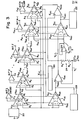
- Fig. 3 shows an absolute-value A/D converter for converting analog voltage signal V I into a digital signal represented by bits 1-N.
- a sanple-and-hold/level shift circuit 20 operates on analog signal V I to produce analog signal V I1 which is the actual signal converted into the digital signal.
- Circuit 20 may be conventional in design but is preferably a sample-and-hold circuit with associated level shift as disclosed in co-filed U.S. patent application PHA 1085, "Impedance Buffer with Reduced Settling Time", the contents of which are incorporated by reference herein.
- This converter contains N main absolute-value gain-of-2 differential amplifiers A 1 , ... A J , ... A N-1 , and A N and corresponding comparators C 1 , ... C J , ... CN-1, and C N which provide the N bits of the digital signal.
- Amplifiers A 1 -A N are powered by the V CC supply and matched to one another. "Matched” here means configurationally the same (except perhaps for minor items which do not affect the pertinent operation) and subjected to substantially the same temperature variation. Matched items are usually, though not necessarily, substantially the same in a tophographical sense -- e.g., laid out the same on a semiconductor wafer and oriented in the same direction.
- Analog signal V I1 is the mainline input to amplifier A 1 .
- Each amplifier A J generates its output signal V CJ by amplifying the absolute value of the voltage difference between its mainline input signal V IJ and its reference input signal.
- Each input V IJ is in the range of V L to V U , of which both vary slightly here.
- the reference inputs to amplifiers A 1 -A N are all (V U +V L )/2 which likewise varies slightly. Except for amplifier A N , output V OJ of each amplifier A J is input V IJ+1 to next amplifier A J+1' As to amplifier A N ' its output V ON is not employed in the A/D conversion but may be used as a circuit test point.
- Each amplifier A J consists of a differential amplifying portion D J and an absolute-value buffer portion B J , both shown in dashed lines.
- Differential portion D J whose nominal gain is slightly over 2 amplifies the voltage difference between inputs V IJ and (V U +V L )/2 to generate a pair of signals V AJ and V BJ .
- Buffer B J whose nominal gain is slightly under 1 generates output V QJ by determining the absolute value of the voltage difference between signals V AJ and V BJ .
- Comparator C J generates bit J by comparing them to determine which is greater.
- the transfer function (V OJ ) for each anplifier A J is G
- the gain G which is substantially the same for all amplifiers A 1 -A N since they are matched, is the sum of the desired gain of 2 and a gain error ⁇ G.
- ⁇ V IJ is the difference between V IJ and (V U +V L )/2.
- the voltage offset V OS which is virtually the same for all amplifiers A 1 -A N because of the matching, is ideally zero.
- each amplifier A GC or A OC contains a differential portion D GC or D OC and a buffer portion B GC or B OC corresponding respectively to portions D J and B in amplifier A J .
- amplifier A GC In the gain-control system, amplifier A GC generates an auxiliary output voltage signal V OGC in response to a pair of input signals which differ by (V U -V L )/2--i.e., half of the V L -toV U voltage range. Preferably these input signals are at the V U and (V U +V L )/2 levels.
- Output V OGC is supplied principally to the inverting input of an operational amplifier E GC and also to an impedance matching circuit 22.
- the combination of amplifier E GC and circuit 22 has substantially the same input impedance as amplifier AJ so that the output V OGC effectively "sees" amplifier A J .
- Signal V U is also supplied as a baseline signal to the non-inverting input of amplifier E GC .
- the gain control works in the following manner. Assume that gain error ⁇ G is non-zero, while offset V OS is zero. Since the input difference to amplifier A GC is (V U -V L ) /2, output V OGC is V U + ⁇ G(V U -V L )/2 Accordingly, the input voltage difference to amplifier E GC is - ⁇ G(V U -V L )/2 which causes control voltage V EGC to drop below its nominal value if a G is positive and to rise above its nominal value if ⁇ G is negative. By virtue of the feedback loop to amplifier A GC ' a decrease in control signal V EGC below its nominal value causes the gain of amplifier A GC to decrease, and vice versa. Its gain thereby stabilizes very close to the desired gain of 2. Because amplifiers A 1 -A N and A OC are matched to amplifier A GC and receive control signal V EGC ' their gains also stabilize very near 2.
- V U is supplied from the upper end of a voltage divider 24 whose lower end supplies end-point signal V L and is coupled through a current source I R to the V EE supply.
- Divider 24 consists of resistors R U and R L whose resistances are the same.
- a low-current signal (V U +V L )/2 is provided from the mid-point of divider 24 to the non-inverting input of an operational amplifier 26 whose output if fed back to its inverting input so that amplifier 26 has a closed-loop gain of 1.
- the output of amplifier 26 is voltage (V U +V L )/2 which is at a sufficiently high current level to drive the A 1 -A N , A GC ' and A OC inputs that are at (V U +V L )/2,
- amplifier A OC receives a pair of input signals at the same value. So as to most closely duplicate the average condition in amplifier A 1 utilized in generating the most significant bit, this value is preferably (V U +V L )/2. As a result, amplifier A OC generates a further output voltage signal V OOC that equals V L + V OS .
- Output V OOC is supplied to the non-inverting input of an operational amplifier E OC and also to an impedance matching circuit 28.
- the combination of amplifier E OC and circuit 28 duplicates the input impedance of amplifier A J ' causing output V OOC to effectively "see" amplifier A J .
- End point V L is supplied from divider 24 to the inverting input of amplifier E OC . Consequently, the input voltage difference to amplifier E OC is offset V OS . Responsive to this difference, amplifier E OC generates an offset-control (error) signal which is baseline voltage V U at the top of divider 24 here. In this way, amplifier E OC also provides the supply voltage for divider 24.
- the offset control works in the following way.
- Amplifier E OC causes voltage V U to rise above its nominal level when offset V OS is pcsitive, and vice versa.
- the voltage at each point on divider 24 changes by the same amount, In particular, signals V L and (V U +V L )/2each change by this amount.
- V OOC Assuming output V OOC to be constant, adjustment of voltage V L resulting from its feedback to amplifier E OC regulates offset V OS . This occurs because amplifier E OC can tolerate only an extremely small input voltage difference. V OOC which equals V L + V OS then equates to signal V L . Accordingly, end point V L appropriately adjusts to force offset V OS toward zero. Since amplifiers A 1 -A N and A GC are matched to amplifier A OC , their offsets likewise closely approach zero.
- output V OOC does vary. Its variance is regulated in a manner that causes voltage (V U +V L )/2 to reach a value suitable for the operation of amplifiers A 1 -A N .
- Amplifiers A GC and E GC are involved here. Excluding any gain change, output V OGC does not change when signal V U changes since the difference between signals V U and (V U +V L )/2 is constant.
- the input voltage difference to amplifier E GC then increases to raise control signal V EGC when offset V OS is positive, and vice versa.
- the change in voltage V EGC which is fed back to the gain-control input of amplifier A OC causes the V L term in output V OOC to change.
- amplifier E OC and divider 24 provide signal (V U +V L )/2 at an acceptable level.
- This converter also contains a linearity control 30 which generates a linearity-control voltage signal V LC that is supplied to the current-control inputs of buffers B 1 -B N , B GC , and B OC in amplifiers A 1 -A N , A GC , and A OC .
- Control voltage V LC is suitably adjusted so as to induce a linear relationship between output V OJ or V GC and the absolute value of the input voltage difference to each amplifier A J or A GC .
- Fig. 4 shows the circuitry for a cell containing each main amplifier A J and its associated comparator C J plus the circuitry for linearity control 30 employed in Fig. 3.
- the circuitry employed for amplifier A is also employed for amplifiers A GC and A OC. For convenience, they are laid out in a integrated circuit in cells indentical to the AJ cell. That is, the portion of the circuitry not used for the absolute-value differential amplifying function in the A GC and A GC cells is also laid out but is inactive.
- the transistors shown in Fig. 4 are all NPN bipolar transistors having the same emitter area.
- Amplifier A J contains transistors Q1 A and Q1 B as the active part of differential portion D J , resistors R1 A and R1 B which have the same resistance R 1 , transistors Q2 A and Q2 B as the active part of buffer B J , resistors R2 A and R2 B which have the same resistance R 2 , resistors R3 A and R3 B which have the same resistance R 3 , the current source formed by transistor Q3 and resistor R G , and the current source formed by transistor Q4 and resistor R B . These elements are connected as shown in Fig. 4 and also as described above for Fig. 2. (Resistor R A is absent in Fig.
- Voltages V AJ and V BJ are respectively supplied from the Q A and Q B collectors.
- Voltage V EGC is supplied to the base of transistor Q3 to control the gain current I G for differential portion D J .
- the gain is approximately (R 2 +R 3 )/2 (P 1 +kT/qI g ) where k is Boltzmann's constant, T is the device temperature, and q is the electronic charge.
- Voltage V LC is supplied to the base of transistor Q4 to control the buffer current I B for buffer B J .
- Buffer current I B may be expressed as CkT/qR 3 where C is a constant. The linearity is best when C is in the range of 1.5-1.7 and is very near 1.6. Linearity control 30 regulates current I B so as to bring it very close to the optimum value.
- Circuit 30 contains transistors Q5 and Q6 whose bases are coupled together through a node 32.
- the Q5 emitter area differs from and is normally greater than the Q6 emitter area by a factor M C which is optimally 5.
- transistor Q5 is represented as having multiple emitters, it is normally laid out as a group of parallel transistors each having the same emitter area as transistor Q6.
- a resistor R4 having a resistance R4 is coupled between the V EE supply and the Q5 emitter.
- Resistors R5 C and R5 D having the same resistance R5 as resistor R B are connected between the V EE supply and the Q5 and Q6 emitters, respectively, resistors R4 and R5 C being in series.
- Resistors R6 C and R6 D having the same resistance R 6 are connected between the V CC supply and the Q5 and Q6 collectors, respectively.
- An operational amplifier E LC supplies control voltage V LC at node 32 to drive the Q5 and Q6 bases.
- the inputs of amplifier E LC are connected to the Q5 and Q6 collectors.
- the E LC input connections could be reversed from those shown.
- a resistor R7 is connected between node 32 and the Q5 base to compensate for base resistance mismatch due to the different areas of transistors Q5 and Q6.
- R3 and R 4 are the same.
- M B is 1, while M C is 5. Accordingly, C is 1n5 or about 1.61.
- Fig. 5 illustrates how linearity control 30 interacts with the cross-coupling of transistors Q2 A and Q2 B to provide the proper amount of positive feedback for causing V OJ to vary linearly with
- Curve 34 which rounds off near the point at which input V IJ equals the reference input represents the case where there is insufficient or no feedback.
- Curve 36 which forms a cusp represents the situation where there is too much feedback.
- Curve 38 respresents the case in which there is precisely the proper amount of feedback.
- each amplifier A J also serves as part of associated comparator C J . This is accomplished with a corresponding switch S J containing transistors Q7 H and Q7 S connected between the Q3 collector and nodes 16 and 18, respectively.
- a voltage V H drives the base of transistor Q7 H .
- a complementary voltage V S drives the base of transistor Q7 S .
- Amplifier A J is switched to its comparing mode by dropping voltage V H to the low voltage to turn off transistor Q7 H . This cuts off the operating current to transistors Q1 A and Q1 B . They turn off to prevent inputs V IJ and (V U +V L ) /2 from affecting transistors Q2 A and Q2B. At the same time, signal V S is raised to the high voltage to turn on transistor Q7 S . This enables the current from the Q3 current source to switch to transistors Q2 and Q2B so as to further amplify the amplified voltage difference at their bases.
- Transistors Q2 A and Q2 B latch in either a binary "0" logic state or a binary logic state depending on whether mainline signal V IJ exceeded reference signal (V U +V L )/2 or not just before signal V S went high. Signals V AJ and. V BJ now serve as complementary signals representative of the A J logic state.
- Each comparator C J preferably also includes a corresponding comparing amplifier F J for amplifying the voltage difference between signals V AJ and V BJ when amplifier A J is being operated as a latch. Comparing amplifier F J converts this amplified voltage difference into a current output signal I OJ that represents bit J of the digital signal. Amplifier F J also provides a current output signal I OJ complementary to output I OJ . When amplifier A J is in its amplifying mode, switch S J causes amplifier F J to latch signals I OJ and I OJ .
- Amplifier F J contains a pair of differential-input transistors Q8 E and Q8 F interconnected through a node 40, a pair of cross-coupled storage transistors Q9 E and Q9 F interconnected through a node 42, resistors R8 E and R8 F having the same resistance R 8 , a current source formed by a transistor Q10 and a series resistor R9, a pair of output transistors Q11 E and Q11 F , and a current source formed by a transistor Q12 and a series resistor R 10 , all connected as shown in Fig. 4.
- a voltage such as voltage V LC drives the Q10 current source.
- a bias voltage V B drives the Q12 current source.
- Switch S J in comparator C J further includes a pair of transistors Q13 H and Q13 S whose bases respectively receive signals V H 5 and V S .
- Transistors Q13 H and Q13 S are connected between the Q10 collector and nodes 42 and 40, respectively, as shown in Fig. 4.
- Transistor Q13 S turns off when signal V S goes low. This turns off transistors Q8 E and Q8 F to prevent voltages V AJ and V BJ from affecting amplifier F J . Simultaneously, transistor Q13 H goes on as signal V H goes high. This turns on transistors Q9 E and Q9 F . Because they are cross-coupled, they latch at either a "0" or "1" depending on whether voltage V AJ exceeded voltage V BJ or not when signal V H went high. The Q9 F and Q9 E collectors then drive transistors Q11 F and Q11 F to force them to continue to provide the data bit and its complement to output I OJ and I OJ .
- Switch S J is preferably operated in coordination with sample-and-hold/level shift circuit 20.
- circuit 20 holds input V I1 at the current value.
- amplifiers A1-A N are in their amplifying mode while amplifiers F 1 -F N are operating as latches to provide the digital signal of the prior sampling.
- signal V H goes low, circuit 20 allows analog signal V I to be sampled.
- Amplifiers A 1 -A N then latch while amplifiers F 1 -F N receive and amplify their data bits to provide the digital signal.
- signal V H goes high again, amplifiers F 1 -F N latch to continue providing the same digital signal.
- N is 8.
- Voltages V CC and V EE are 5 and -5 volts, respectively.
- Bias voltage V B is -4 volts.
- Resistors R U and R L are each 250 ohms.
- Current source I R is 1 milliampere.
- Resistor R B which equals R 5 is 1,000 ohms.
- Resistors R G , R7, R9, and R10 are each 500 ohms.
- Each operational amplifier E GC , E OC , 26, or E LC is conventional in design and has an open-loop gain greater than 10,000.
- Fig. 6 shows another A/D converter having a feedback control system for causing the gains of matched amplifiers A 1 -A N to closely approach 2 and for making their offsets very small.
- Each amplifier A J and its associated comparator C J are preferably configured and operable the same as described for Figs. 3 and 4.
- the control system of Fig. 6 again utilizes amplifiers A GC and A OC which are matched to amplifiers A 1 -A N and are internally configured and operable the same as amplifier A J .
- This control system also contains amplifiers E GC and E OC which operate between the V and V supplies.
- the converter of Fig. 6 contains linearity control 30 configured and operable the same as in Figs. 3 and 4. For simplicity, circuits 20, 22, and 28 are not shown in Fig. 6 although they are employed in this converter.
- voltages V L , (V U +V L )/2, and V U are fixed values preferably generated from an external voltage divider (not shown).
- Signal (V U +V L )/2 is again provided as the reference input to each amplifier A J , as one of the inputs to amplifier A GC , and as both inputs to amplifier A OC .
- the other input to amplifier A GC is again signal V U .
- the gain-control system here is largely separate from the offset-control system.
- amplifiers A GC and E GC function in the same manner as described for Fig. 3.
- amplifier A OC again provides output V OOC at a value of V L + V OS .
- V OOC and end point V L supplied respectively to the inverting and non-inverting inputs of amplifier E OC it generates an offset-control (error) signal V EOC which is fed back to the supply voltage input of amplifier A OC .
- V OS If offset V OS is positive, supply voltage V EOC decreases. This forces offset V downward toward zero. The reverse occurs if V OS is negative.
- Control signal V EOC is provided as the supply voltage to amplifiers A 1 -A N and A GC and thereby forces their offsets toward zero because of the matching.
- V EOC and V OOC are respectively substi- tuted for V CC and V OJ in F ig. 4, V OOC equals V EOC - K, where K is a constant since the inputs to amplifier A OC are balanced. Accordingly, V EOC - V OS is equal to V L + K. Since VL is also constant here, decreasing output V OOC decreases offset V OS , and vice versa.
- Fig. 7 illustrates another absolute-value A/D converter having a composite feedback system for gain/offset control generally of the type described for Fig. 3. The principal difference is that this converter uses a different absolute-value algorithm.
- the prime notation is employed in Fig. 7 to indicate elements that differ in some way from those of Fig. 3. The elements operating the same as in Fig. 3 are largely not discussed here.
- a chain of matched absolute-value differential amplifiers A1'-A N ' performs the A/D conversion in combination with corresponding comparators C 1 -C N .
- the gain/offset control system utilizes absolute-value differential amplifiers A GC ' and A OC ' matched to amplifiers A 1 '-A N '.
- Each amplifier A J ' , A GC ' , or A OC is internally configured and basically operable the same as respective amplifier A J , A GC , or A OC of Figs. 3 and 4.
- Amplifiers A '-A N ', A GC ', and A OC all have the same gain.
- Linearity control 30 operates the same as in Figs. 3 and 4. Circuits 20, 22, and 28 are also incorporated in this converter although not shown in Fig. 7.
- each amplifier A J ' , A GC ' , or A OC ' is different from 2. This is done by changing the values given above for some of the absolute-value amplifier resistors shown in Fig. 4.
- Each main amplifier A J ' receives a reference input signal V RJ normally different from that supplied to each other main amplifier A J '.
- Each reference input V RJ is provided from the lower end of a resistor R J ' in a set of upper resistors R 1 '-R N ' in a voltage divider 44 also including a lower resistor R O '.
- Signal V U is supplied to the upper end of divider 44 while its lower end provides signal V L and is coupled through a current source I R ' to the V EE supply.
- Auxiliary amplifier A GC ' receives a pair of input signals from different points on divider 44, while further amplifier A OC ' receives a pair of input signals at the same value provided from a point on divider 44.
- this D/A converter might use an absolute-value algorithm in which amplifiers A 1 '-A N ', A GC ', and A OC ' all have a desired gain of 1. (Although "buffers" might perhaps be a better description here for elements A 1 ' - AN ', AGe and A OC ', they are still referred to categorically as "amplifiers" in semiconductor language.)
- each input V RJ is V L + (V U -V L )/2 J .
- the resistance of each resistor R J ' in divider 44 is 2 N - J times that of resistor R O '.
- the gain-control system in Fig. 7 operates in the same manner as in Fig. 3.
- the same type of feedback path to the gain-control input of amplifier A GC ' forces its gain toward the desired gain. Branches of this path to the gain-control inputs of amplifiers A 1 '-A N ' and A OC ' then force their gains toward the desired gain as a result of the amplifier matching.
- the offset-control system of Fig. 7 also operates in the same manner as in Fig. 3.
- Amplifier A OC again supplies output V OOC at a value of V L + V OS .
- amplifier E OC Responsive to the voltage difference between signals V OOC and V , amplifier E OC generates voltage V U at the top of divider 44.
- Signal V U differs from its nominal value when offset V OS is non-zero. This difference is reflected at each point along divider 44, including end point V L .
- the V L feedback to amplifier E G C causes it to adjust signal V u (and also signal V L ) to make offset V OS closely approach zero.
- the offsets of amplifiers A1'-A N ' and A GC ' are then driven toward zero because of the matching.
- the values of reference inputs V R1 V RN suitable for the operation of amplifiers A1'-A N ' are determined by a control path further involving amplifiers A GC ' and E analogous to that described for Fig
Landscapes
- Engineering & Computer Science (AREA)
- Theoretical Computer Science (AREA)
- Analogue/Digital Conversion (AREA)
- Amplifiers (AREA)
Applications Claiming Priority (2)
| Application Number | Priority Date | Filing Date | Title |
|---|---|---|---|
| US06/468,720 US4593268A (en) | 1983-02-22 | 1983-02-22 | Analog-to-digital converter using absolute-value conversion |
| US468720 | 1983-02-22 |
Publications (2)
| Publication Number | Publication Date |
|---|---|
| EP0117007A2 true EP0117007A2 (fr) | 1984-08-29 |
| EP0117007A3 EP0117007A3 (fr) | 1988-07-27 |
Family
ID=23860968
Family Applications (1)
| Application Number | Title | Priority Date | Filing Date |
|---|---|---|---|
| EP84200218A Withdrawn EP0117007A3 (fr) | 1983-02-22 | 1984-02-20 | Convertisseur analogique-numérique utilisant la conversion de valeur absolue |
Country Status (4)
| Country | Link |
|---|---|
| US (1) | US4593268A (fr) |
| EP (1) | EP0117007A3 (fr) |
| JP (1) | JPS59191928A (fr) |
| CA (1) | CA1224275A (fr) |
Cited By (1)
| Publication number | Priority date | Publication date | Assignee | Title |
|---|---|---|---|---|
| CN101933228B (zh) * | 2008-02-06 | 2013-05-08 | 高通股份有限公司 | 具有失真后模式和高增益模式的低噪声放大器及其控制方法 |
Families Citing this family (11)
| Publication number | Priority date | Publication date | Assignee | Title |
|---|---|---|---|---|
| US4799041A (en) * | 1986-10-06 | 1989-01-17 | Applied Automation, Inc. | Recirculating analog to digital converter with auto-calibrating feature |
| US4978959A (en) * | 1987-10-08 | 1990-12-18 | University Of Toronto Innovations Foundation | Analog to digital converter, a digital to analog converter and an operational amplifier therefor |
| US5107265A (en) * | 1988-12-15 | 1992-04-21 | Schlumberger Technologies Limited | Analog to digital converter |
| JPH0470214A (ja) * | 1990-07-11 | 1992-03-05 | Inter Nitsukusu Kk | A/dコンバータ |
| EP0517305B1 (fr) * | 1991-06-03 | 1995-11-22 | Koninklijke Philips Electronics N.V. | Amplificateur et détecteur logarithmique |
| DE69223212T2 (de) * | 1991-08-15 | 1998-05-14 | Texas Instruments Inc | Kalibrierung eines aus einer rekonfigurierbaren Reihe von Stufen bestehenden Systems |
| US5296761A (en) * | 1992-11-23 | 1994-03-22 | North American Philips Corporation | Temperature-compensated logarithmic detector having a wide dynamic range |
| DE69316569T2 (de) * | 1992-12-23 | 1998-08-20 | Eastman Kodak Co | Automatischer Abgleich der Kanalverstärkung und -abweichung für Videokameras mit Multikanalsensoren |
| US5499027A (en) * | 1994-02-24 | 1996-03-12 | Massachusetts Institute Of Technology | Digitally self-calibrating pipeline analog-to-digital converter |
| US6710735B1 (en) * | 2003-06-17 | 2004-03-23 | Realter Semiconductor Corp. | Dual supply voltage pipelined ADC |
| US9993386B2 (en) * | 2013-11-29 | 2018-06-12 | Louis G. RACETTE | Instrumentation absolute value differential amplifier circuit and applications |
Family Cites Families (3)
| Publication number | Priority date | Publication date | Assignee | Title |
|---|---|---|---|---|
| JPS4932227A (fr) * | 1972-07-25 | 1974-03-23 | ||
| US4353059A (en) * | 1980-05-16 | 1982-10-05 | Motorola Inc. | Multithreshold converter utilizing reference tracking amplifiers |
| JPS5722441A (en) * | 1980-07-16 | 1982-02-05 | Nissan Motor Co Ltd | Transmission v-belt |
-
1983
- 1983-02-22 US US06/468,720 patent/US4593268A/en not_active Expired - Fee Related
-
1984
- 1984-02-16 CA CA000447570A patent/CA1224275A/fr not_active Expired
- 1984-02-20 EP EP84200218A patent/EP0117007A3/fr not_active Withdrawn
- 1984-02-22 JP JP59030443A patent/JPS59191928A/ja active Pending
Cited By (1)
| Publication number | Priority date | Publication date | Assignee | Title |
|---|---|---|---|---|
| CN101933228B (zh) * | 2008-02-06 | 2013-05-08 | 高通股份有限公司 | 具有失真后模式和高增益模式的低噪声放大器及其控制方法 |
Also Published As
| Publication number | Publication date |
|---|---|
| EP0117007A3 (fr) | 1988-07-27 |
| JPS59191928A (ja) | 1984-10-31 |
| US4593268A (en) | 1986-06-03 |
| CA1224275A (fr) | 1987-07-14 |
Similar Documents
| Publication | Publication Date | Title |
|---|---|---|
| EP0108428B1 (fr) | Circuit amplificateur différentiel dont la gamme de tension d'entrée est égale à la tension d'alimentation | |
| US4763107A (en) | Subranging analog-to-digital converter with multiplexed input amplifier isolation circuit between subtraction node and LSB encoder | |
| US4599602A (en) | Serial-type A/D converter utilizing folding circuit cells | |
| US4593268A (en) | Analog-to-digital converter using absolute-value conversion | |
| US3914683A (en) | Current stabilizing arrangement with resistive-type current amplifier and a differential amplifier | |
| US4573005A (en) | Current source arrangement having a precision current-mirror circuit | |
| US20010004219A1 (en) | Low voltage differential signal (LVDS) input circuit | |
| JPS61210723A (ja) | デジタル‐アナログ変換器 | |
| US4686511A (en) | Subranging analog-to-digital converter with FET isolation circuit between subtraction node and LSB encoder | |
| US6028459A (en) | Track and hold circuit with clamp | |
| JPH09512684A (ja) | 低電圧cmosコンパレータ | |
| US4634993A (en) | High gain, low drift operational amplifier for sample and hold circuit | |
| US3673508A (en) | Solid state operational amplifier | |
| JPS58138122A (ja) | 並列型アナログ・デイジタル変換器 | |
| US4833422A (en) | Programmable gain instrumentation amplifier | |
| HK5394A (en) | A current to voltage converter circuit | |
| US4571507A (en) | Successive approximation analog-to-digital converter | |
| US4381497A (en) | Digital-to-analog converter having open-loop voltage reference for regulating bit switch currents | |
| US4460873A (en) | Active differential output direct current offset voltage compensation circuit for a differential amplifier | |
| US4888589A (en) | Digital-to-analog converter with diode control | |
| US4283673A (en) | Means for reducing current-gain modulation due to differences in collector-base voltages on a transistor pair | |
| US4034366A (en) | Analog-to-digital converter with controlled ladder network | |
| USRE29619E (en) | Constant-current digital-to-analog converter | |
| US5550492A (en) | Analog to digital converter using complementary differential emitter pairs | |
| US5113146A (en) | Amplifier arrangement |
Legal Events
| Date | Code | Title | Description |
|---|---|---|---|
| PUAI | Public reference made under article 153(3) epc to a published international application that has entered the european phase |
Free format text: ORIGINAL CODE: 0009012 |
|
| AK | Designated contracting states |
Designated state(s): DE FR GB IT |
|
| PUAL | Search report despatched |
Free format text: ORIGINAL CODE: 0009013 |
|
| AK | Designated contracting states |
Kind code of ref document: A3 Designated state(s): DE FR GB IT |
|
| 17P | Request for examination filed |
Effective date: 19890125 |
|
| 17Q | First examination report despatched |
Effective date: 19900408 |
|
| STAA | Information on the status of an ep patent application or granted ep patent |
Free format text: STATUS: THE APPLICATION IS DEEMED TO BE WITHDRAWN |
|
| 18D | Application deemed to be withdrawn |
Effective date: 19900829 |
|
| RIN1 | Information on inventor provided before grant (corrected) |
Inventor name: BLAUSCHILD, ROBERT ALAN |