EP0117348B1 - Procédé pour souder des fils aux composants semi-conducteurs - Google Patents
Procédé pour souder des fils aux composants semi-conducteurs Download PDFInfo
- Publication number
- EP0117348B1 EP0117348B1 EP83307382A EP83307382A EP0117348B1 EP 0117348 B1 EP0117348 B1 EP 0117348B1 EP 83307382 A EP83307382 A EP 83307382A EP 83307382 A EP83307382 A EP 83307382A EP 0117348 B1 EP0117348 B1 EP 0117348B1
- Authority
- EP
- European Patent Office
- Prior art keywords
- tape
- leads
- lead
- bumps
- accordance
- Prior art date
- Legal status (The legal status is an assumption and is not a legal conclusion. Google has not performed a legal analysis and makes no representation as to the accuracy of the status listed.)
- Expired
Links
Images


Classifications
-
- H—ELECTRICITY
- H10—SEMICONDUCTOR DEVICES; ELECTRIC SOLID-STATE DEVICES NOT OTHERWISE PROVIDED FOR
- H10W—GENERIC PACKAGES, INTERCONNECTIONS, CONNECTORS OR OTHER CONSTRUCTIONAL DETAILS OF DEVICES COVERED BY CLASS H10
- H10W72/00—Interconnections or connectors in packages
- H10W72/071—Connecting or disconnecting
- H10W72/077—Connecting of TAB connectors
-
- B—PERFORMING OPERATIONS; TRANSPORTING
- B23—MACHINE TOOLS; METAL-WORKING NOT OTHERWISE PROVIDED FOR
- B23K—SOLDERING OR UNSOLDERING; WELDING; CLADDING OR PLATING BY SOLDERING OR WELDING; CUTTING BY APPLYING HEAT LOCALLY, e.g. FLAME CUTTING; WORKING BY LASER BEAM
- B23K20/00—Non-electric welding by applying impact or other pressure, with or without the application of heat, e.g. cladding or plating
- B23K20/24—Preliminary treatment
-
- H—ELECTRICITY
- H05—ELECTRIC TECHNIQUES NOT OTHERWISE PROVIDED FOR
- H05K—PRINTED CIRCUITS; CASINGS OR CONSTRUCTIONAL DETAILS OF ELECTRIC APPARATUS; MANUFACTURE OF ASSEMBLAGES OF ELECTRICAL COMPONENTS
- H05K13/00—Apparatus or processes specially adapted for manufacturing or adjusting assemblages of electric components
- H05K13/04—Mounting of components, e.g. of leadless components
- H05K13/046—Surface mounting
- H05K13/0465—Surface mounting by soldering
-
- H—ELECTRICITY
- H10—SEMICONDUCTOR DEVICES; ELECTRIC SOLID-STATE DEVICES NOT OTHERWISE PROVIDED FOR
- H10W—GENERIC PACKAGES, INTERCONNECTIONS, CONNECTORS OR OTHER CONSTRUCTIONAL DETAILS OF DEVICES COVERED BY CLASS H10
- H10W70/00—Package substrates; Interposers; Redistribution layers [RDL]
- H10W70/01—Manufacture or treatment
- H10W70/04—Manufacture or treatment of leadframes
-
- H—ELECTRICITY
- H10—SEMICONDUCTOR DEVICES; ELECTRIC SOLID-STATE DEVICES NOT OTHERWISE PROVIDED FOR
- H10W—GENERIC PACKAGES, INTERCONNECTIONS, CONNECTORS OR OTHER CONSTRUCTIONAL DETAILS OF DEVICES COVERED BY CLASS H10
- H10W70/00—Package substrates; Interposers; Redistribution layers [RDL]
- H10W70/40—Leadframes
- H10W70/453—Leadframes comprising flexible metallic tapes
-
- H—ELECTRICITY
- H10—SEMICONDUCTOR DEVICES; ELECTRIC SOLID-STATE DEVICES NOT OTHERWISE PROVIDED FOR
- H10W—GENERIC PACKAGES, INTERCONNECTIONS, CONNECTORS OR OTHER CONSTRUCTIONAL DETAILS OF DEVICES COVERED BY CLASS H10
- H10W72/00—Interconnections or connectors in packages
- H10W72/701—Tape-automated bond [TAB] connectors
Definitions
- the interconnection of integrated circuit devices is necessary during the manufacture of hybrid and discrete devices. Such interconnection is generally accomplished by wire bonding, a process which is inherently slow because each wire has to be welded individually.
- Automatic wire bonding machines are capable of forming connections to devices at up to 10 loops per second when using 25 pm diameter wire.
- Various techniques have been devised to increase the speed of the operation by making several joints at the same time and to improve the reliability of the micro-circuit interconnections. The most successful of these has been a process wich has become known as tape automated bonding (TAB).
- TAB tape automated bonding
- the leads are fabricated in a continuous film and in each operation the free ends of leads are connected to metallic bonding projections ("bumps") on the semiconductor chip.
- the tapes are available in three forms, as shown in Figures 1a, 1b and 1c.
- a single layer of metal foil for example, copper or aluminium foil, exists in the form of a tape, the metal foil being etched to form the required pattern of separate leads, which are of course interconnected to form the tape.
- this single-layer tape does not allow pre-testing of the device.
- the ends of the single tape layer 10 have been bonded to the bumps 12 on the chip 14, the interconnecting portions of the tape are cut away to separate the leads.
- FIG. 1b A two-layer form of tape is illustrated in Figure 1b.
- This comprises a laminate of copper and an insulator of plastics material.
- the insulator may for example be a film of polyimide bonded directly to the metal foil leads. This is available in both testable and untestable formats.
- the dielectric film 16 is usually thicker and is joined to the metal foil by means of a layer 18 of an adhesive.
- each frame of the film has sprocket holes for indexing and registration.
- the plastics film is formed with windows 17 and the ends of the leads 10 which are to be connected to the bumps 12 on the chip 14 overhang the edge of a window.
- the bumps provide both the necessary bonding metallurgy and compliance for inner lead bonding and the physical spacing to prevent short-circuiting of the lead to the chip.
- Figure 2 shows the manner in which the bump is typically applied to the silicon chip.
- a three- level metallisation consisting of an aluminium pad 20, a layer 22 of adhesion metal and a layer 24 of diffusion barrier metal is first applied to the chip 14, after which the bump 12 of copper, gold or tin/lead is electro-plated over the barrier metallisation to form a contact pad for the tape of copper or tin- or gold-plated copper.
- a number of leads are simultaneously bonded to their respective bumps, usually by thermocompression, eutectic or solder-reflow bonding, depending on the tape and bump metallurgies.
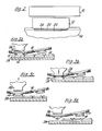
- Figure 3 illustrates a typical bonding sequence.
- a heated tool or electrode 26 descends through a window in the film 16, pressing the inner leads against the bumps to form a bond.
- the chip is released from the underlying wax layer 28 by the heat of the operation ( Figure 3c) and a new set of inner leads are brought into position for bonding to the bumps on a new chip ( Figure 3d).
- the heated tool then again descends through a window in the film 16 to make a fresh set of bonds.
- bumped tape automated bonding BTAB
- BTAB bumped tape automated bonding
- the bumped tape is illustrated in Figure 4; the bump 12a was formed by selectively etching the metal tape.
- a single-layer copper tape of 70 um thickness is etched to a thickness of 35 um for the leads, with an extra 35 um of thickness for the bumps.
- a plating process can be used in place of the etching process; the plating process is more likely to be used when gold bumps are to be added to the metal tape than when copper bumps are required.
- the bumped tape process has encountered problems in that it is difficult to produce bumps of consistent size, surface topography and hardness, and as a consequence inconsistent bonding occurs.
- a method of forming connecting bumps on the free ends of the conductive leads of a tape for use in the bumped-tape automated bonding process of connecting leads to a semi-conductor circuit device includes heating the free ends of the leads on the tape by means of a laser beam to melt the ends of the leads so that surface-tension forces form the liquid-phase end of each lead into a ball, constituting the bonding bump. Thereafter bonding the bumped ends of the leads of the tape to terminals of the device may be accomplished by conventional techniques.
- the bumps may be applied to the leads by the tape manufacturer.
- connections to the chip may be formed by a method similar to that illustrated in Figure 3.
- the chips are carried, on the tape, to a station at which the outer lead bonds are made to a printed circuit board or other carrier.
- the insulating film is then removed to enable the outer bonds to be made.
- the laser used in the method illustrated in Figure 5 is preferably a pulsed Nd/YAG laser, but other lasers (for example CO2), with a pulsed or continuous-wave output may be used.
- a single pulse of the laser beam may be directed at each lead or finger with the tape stationary, the beam then moving on to the next lead or finger; alternatively, the tape may be moved at a uniform speed under a rapidly pulsed beam.
- a tape moved at uniform speed may also be used in conjunction with a continuous wave beam.
- the laser beam itself may be moved by means of mirrors. Because the metal foils used for the tape (such as copper and aluminium foils) are highly reflective, the focus for the laser beam should be at or close to the surface of the leads or fingers. For some materials, an inert gas shield may be required.
- the present invention may be used with any of the forms of tape illustrated in Figures 1a to 1c.
Landscapes
- Engineering & Computer Science (AREA)
- Mechanical Engineering (AREA)
- Manufacturing & Machinery (AREA)
- Microelectronics & Electronic Packaging (AREA)
- Wire Bonding (AREA)
- Laser Beam Processing (AREA)
Claims (7)
Applications Claiming Priority (2)
| Application Number | Priority Date | Filing Date | Title |
|---|---|---|---|
| GB8234733 | 1982-12-06 | ||
| GB8234733 | 1982-12-06 |
Publications (2)
| Publication Number | Publication Date |
|---|---|
| EP0117348A1 EP0117348A1 (fr) | 1984-09-05 |
| EP0117348B1 true EP0117348B1 (fr) | 1987-03-11 |
Family
ID=10534773
Family Applications (1)
| Application Number | Title | Priority Date | Filing Date |
|---|---|---|---|
| EP83307382A Expired EP0117348B1 (fr) | 1982-12-06 | 1983-12-05 | Procédé pour souder des fils aux composants semi-conducteurs |
Country Status (4)
| Country | Link |
|---|---|
| US (1) | US4587395A (fr) |
| EP (1) | EP0117348B1 (fr) |
| JP (1) | JPS59110128A (fr) |
| DE (1) | DE3370240D1 (fr) |
Families Citing this family (21)
| Publication number | Priority date | Publication date | Assignee | Title |
|---|---|---|---|---|
| EP0209650A3 (fr) * | 1985-06-07 | 1989-07-05 | Vanzetti Systems, Inc. | Méthode et appareil pour placer et connecter électriquement des composants sur une plaquette à circuit imprimé |
| NL8501677A (nl) * | 1985-06-11 | 1987-01-02 | Littelfuse Tracor | Werkwijze voor het bevestigen van een aansluitdraad aan een metalen eindkap van een smeltveiligheid. |
| DE3544377A1 (de) * | 1985-12-14 | 1987-06-19 | Bbc Brown Boveri & Cie | Verfahren und vorrichtung zum verbinden eines halbleiters mit anschlussdraehten |
| US4814855A (en) * | 1986-04-29 | 1989-03-21 | International Business Machines Corporation | Balltape structure for tape automated bonding, multilayer packaging, universal chip interconnection and energy beam processes for manufacturing balltape |
| US4845335A (en) * | 1988-01-28 | 1989-07-04 | Microelectronics And Computer Technology Corporation | Laser Bonding apparatus and method |
| US4862322A (en) * | 1988-05-02 | 1989-08-29 | Bickford Harry R | Double electronic device structure having beam leads solderlessly bonded between contact locations on each device and projecting outwardly from therebetween |
| GB8915816D0 (en) * | 1989-07-11 | 1989-08-31 | Welding Inst | Bonding electrical conductors |
| US5008512A (en) * | 1989-09-08 | 1991-04-16 | Microelectronics And Computer Technology Corporation | Method of laser bonding electrical members |
| US5049718A (en) * | 1989-09-08 | 1991-09-17 | Microelectronics And Computer Technology Corporation | Method of laser bonding for gold, gold coated and gold alloy coated electrical members |
| KR940004246B1 (ko) * | 1989-09-11 | 1994-05-19 | 신닛뽕 세이데쓰 가부시끼가이샤 | Tab 테이프와 반도체칩을 접속하는 방법 및 그것에 사용하는 범프시이트와 범프 부착 tab 테이프 |
| DE4017863C1 (fr) * | 1990-06-02 | 1991-07-18 | Du Pont De Nemours (Deutschland) Gmbh, 4000 Duesseldorf, De | |
| US5164566A (en) * | 1990-06-12 | 1992-11-17 | Microelectronics And Computer Technology Corp. | Method and apparatus for fluxless solder reflow |
| US5083007A (en) * | 1990-08-01 | 1992-01-21 | Microelectronics And Computer Technology Corporation | Bonding metal electrical members with a frequency doubled pulsed laser beam |
| US5189261A (en) * | 1990-10-09 | 1993-02-23 | Ibm Corporation | Electrical and/or thermal interconnections and methods for obtaining such |
| US5105062A (en) * | 1990-12-17 | 1992-04-14 | General Electric Company | Method for forming an electrode-lead assembly |
| US5316803A (en) * | 1992-12-10 | 1994-05-31 | International Business Machines Corporation | Method for forming electrical interconnections in laminated vias |
| US6630643B2 (en) * | 2001-07-30 | 2003-10-07 | Cypress Semiconductor Corporation | Method and structure for forming metallic interconnections using directed thermal diffusion |
| ATE474444T1 (de) * | 2002-05-24 | 2010-07-15 | Koninkl Philips Electronics Nv | Verfahren zur übertragung von einem an einen träger befestigten bauelement in eine gewünschte lage auf einen träger und einrichtung dafur |
| US7150594B2 (en) * | 2004-03-09 | 2006-12-19 | The Boeing Company | Hybrid fastener apparatus and method for fastening |
| DE102006044936B4 (de) * | 2006-09-22 | 2008-08-07 | Fraunhofer-Gesellschaft zur Förderung der angewandten Forschung e.V. | Verfahren zur Metallisierung von Solarzellen und dessen Verwendung |
| CN115635210B (zh) * | 2022-12-23 | 2023-06-23 | 湖南湘投金天钛金属股份有限公司 | 一种tc4钛合金板材表层高熵合金改性方法 |
Family Cites Families (7)
| Publication number | Priority date | Publication date | Assignee | Title |
|---|---|---|---|---|
| US3614832A (en) * | 1966-03-09 | 1971-10-26 | Ibm | Decal connectors and methods of forming decal connections to solid state devices |
| US3718968A (en) * | 1969-02-14 | 1973-03-06 | Atomic Energy Commission | Method for connecting a wire to a component |
| JPS5492057A (en) * | 1977-12-28 | 1979-07-20 | Fujitsu Ltd | Manufacture of semiconductor device |
| JPS5562680A (en) * | 1978-10-31 | 1980-05-12 | Ibm | Wire bonding method |
| US4256948A (en) * | 1978-12-15 | 1981-03-17 | Dataproducts Corporation | Integral beaded stylus wire and method of making same |
| DE2919998A1 (de) * | 1979-05-17 | 1980-11-27 | Siemens Ag | Befestigen der anschlussdraehte von halbleitersystemen auf den traegerelementen |
| EP0061852A3 (fr) * | 1981-03-30 | 1983-08-24 | Texas Instruments Incorporated | Appareil de fabrication à arc électrique auto-démarrant et avec réglage de courant pour faire des perles de fils à souder |
-
1983
- 1983-12-05 EP EP83307382A patent/EP0117348B1/fr not_active Expired
- 1983-12-05 DE DE8383307382T patent/DE3370240D1/de not_active Expired
- 1983-12-06 JP JP58229274A patent/JPS59110128A/ja active Pending
- 1983-12-06 US US06/558,625 patent/US4587395A/en not_active Expired - Fee Related
Also Published As
| Publication number | Publication date |
|---|---|
| JPS59110128A (ja) | 1984-06-26 |
| DE3370240D1 (en) | 1987-04-16 |
| EP0117348A1 (fr) | 1984-09-05 |
| US4587395A (en) | 1986-05-06 |
Similar Documents
| Publication | Publication Date | Title |
|---|---|---|
| EP0117348B1 (fr) | Procédé pour souder des fils aux composants semi-conducteurs | |
| US4814855A (en) | Balltape structure for tape automated bonding, multilayer packaging, universal chip interconnection and energy beam processes for manufacturing balltape | |
| EP1226000B1 (fr) | Dispositif et procede de soudage par laser de rubans pour connexions electriques | |
| US6653170B1 (en) | Semiconductor chip assembly with elongated wire ball bonded to chip and electrolessly plated to support circuit | |
| US5260234A (en) | Method for bonding a lead to a die pad using an electroless plating solution | |
| AU610974B2 (en) | Laser bonding apparatus and method | |
| EP0541116B1 (fr) | Procédé pour la liaison d'un conducteur et d'une électrode d'un dispositif électronique | |
| IE53371B1 (en) | Method of providing raised contact portions on contact areas of an electronic microcircuit | |
| US20020076910A1 (en) | High density electronic interconnection | |
| US6350632B1 (en) | Semiconductor chip assembly with ball bond connection joint | |
| GB2261547A (en) | Semiconductor device with bonding pads at the edge | |
| US6511865B1 (en) | Method for forming a ball bond connection joint on a conductive trace and conductive pad in a semiconductor chip assembly | |
| US3914850A (en) | Bonding of dissimilar workpieces to a substrate | |
| JP3021508B2 (ja) | 導電突起の形成方法 | |
| Smith et al. | Hybrid Microcircuit Tape Chip Carrier Materials/Processing Trade-Offs | |
| JPS62234337A (ja) | 半導体装置用フイルムキヤリア | |
| JPH0350736A (ja) | 半導体チップのバンプ製造方法 | |
| JP2798040B2 (ja) | 半導体装置の製造方法 | |
| JP2605999B2 (ja) | 半導体パッケージの製造方法 | |
| Johnson | Microjoining developments for the electronics industry | |
| JP2712595B2 (ja) | 半導体装置の接合方法 | |
| JPH02139944A (ja) | 半導体チップの実装方法 | |
| JPH05145004A (ja) | 半導体装置の製造方法 | |
| JPS6234143B2 (fr) | ||
| JPH04154137A (ja) | フィルムキャリヤーテープの製造方法 |
Legal Events
| Date | Code | Title | Description |
|---|---|---|---|
| PUAI | Public reference made under article 153(3) epc to a published international application that has entered the european phase |
Free format text: ORIGINAL CODE: 0009012 |
|
| AK | Designated contracting states |
Designated state(s): DE FR GB NL |
|
| 17P | Request for examination filed |
Effective date: 19841120 |
|
| 17Q | First examination report despatched |
Effective date: 19860411 |
|
| GRAA | (expected) grant |
Free format text: ORIGINAL CODE: 0009210 |
|
| AK | Designated contracting states |
Kind code of ref document: B1 Designated state(s): DE FR GB NL |
|
| REF | Corresponds to: |
Ref document number: 3370240 Country of ref document: DE Date of ref document: 19870416 |
|
| ET | Fr: translation filed | ||
| PLBE | No opposition filed within time limit |
Free format text: ORIGINAL CODE: 0009261 |
|
| STAA | Information on the status of an ep patent application or granted ep patent |
Free format text: STATUS: NO OPPOSITION FILED WITHIN TIME LIMIT |
|
| 26N | No opposition filed | ||
| PGFP | Annual fee paid to national office [announced via postgrant information from national office to epo] |
Ref country code: GB Payment date: 19901126 Year of fee payment: 8 |
|
| PGFP | Annual fee paid to national office [announced via postgrant information from national office to epo] |
Ref country code: FR Payment date: 19901215 Year of fee payment: 8 |
|
| PGFP | Annual fee paid to national office [announced via postgrant information from national office to epo] |
Ref country code: NL Payment date: 19901231 Year of fee payment: 8 |
|
| PGFP | Annual fee paid to national office [announced via postgrant information from national office to epo] |
Ref country code: DE Payment date: 19910131 Year of fee payment: 8 |
|
| PG25 | Lapsed in a contracting state [announced via postgrant information from national office to epo] |
Ref country code: GB Effective date: 19911205 |
|
| PG25 | Lapsed in a contracting state [announced via postgrant information from national office to epo] |
Ref country code: NL Effective date: 19920701 |
|
| GBPC | Gb: european patent ceased through non-payment of renewal fee | ||
| NLV4 | Nl: lapsed or anulled due to non-payment of the annual fee | ||
| PG25 | Lapsed in a contracting state [announced via postgrant information from national office to epo] |
Ref country code: FR Effective date: 19920831 |
|
| PG25 | Lapsed in a contracting state [announced via postgrant information from national office to epo] |
Ref country code: DE Effective date: 19920901 |
|
| REG | Reference to a national code |
Ref country code: FR Ref legal event code: ST |