EP0118156A1 - Schaltung zur Trägerrückgewinnung für ein in Amplituden- und Phasenstufen moduliertes Signal - Google Patents
Schaltung zur Trägerrückgewinnung für ein in Amplituden- und Phasenstufen moduliertes Signal Download PDFInfo
- Publication number
- EP0118156A1 EP0118156A1 EP84200288A EP84200288A EP0118156A1 EP 0118156 A1 EP0118156 A1 EP 0118156A1 EP 84200288 A EP84200288 A EP 84200288A EP 84200288 A EP84200288 A EP 84200288A EP 0118156 A1 EP0118156 A1 EP 0118156A1
- Authority
- EP
- European Patent Office
- Prior art keywords
- zones
- line
- signal
- carrier
- zone
- Prior art date
- Legal status (The legal status is an assumption and is not a legal conclusion. Google has not performed a legal analysis and makes no representation as to the accuracy of the status listed.)
- Granted
Links
- 230000001419 dependent effect Effects 0.000 claims abstract description 4
- 238000011084 recovery Methods 0.000 claims description 10
- 230000005540 biological transmission Effects 0.000 abstract 1
- 235000021183 entrée Nutrition 0.000 description 16
- 238000005562 fading Methods 0.000 description 3
- 230000001360 synchronised effect Effects 0.000 description 2
- 208000032368 Device malfunction Diseases 0.000 description 1
- 230000015572 biosynthetic process Effects 0.000 description 1
- 230000008929 regeneration Effects 0.000 description 1
- 238000011069 regeneration method Methods 0.000 description 1
Images


Classifications
-
- H—ELECTRICITY
- H04—ELECTRIC COMMUNICATION TECHNIQUE
- H04L—TRANSMISSION OF DIGITAL INFORMATION, e.g. TELEGRAPHIC COMMUNICATION
- H04L27/00—Modulated-carrier systems
- H04L27/32—Carrier systems characterised by combinations of two or more of the types covered by groups H04L27/02, H04L27/10, H04L27/18 or H04L27/26
- H04L27/34—Amplitude- and phase-modulated carrier systems, e.g. quadrature-amplitude modulated carrier systems
- H04L27/38—Demodulator circuits; Receiver circuits
- H04L27/3818—Demodulator circuits; Receiver circuits using coherent demodulation, i.e. using one or more nominally phase synchronous carriers
Definitions
- the invention relates to a device for recovering the carrier of an input signal modulated by amplitude jumps and by phase jumps (in particular MAQ modulation) provided with a frequency-controlled oscillator for producing said carrier, a quadrature detector for supplying signals representing the amplitude of the input signal projected on two components P and Q in quadrature of the signal supplied by said oscillator and for thus determining the states of modulation of the input signal and of correction means to form, from a circuit for determining zones in the plane of the components P and Q, a correction signal for said frequency control of said oscillator.
- a frequency-controlled oscillator for producing said carrier
- a quadrature detector for supplying signals representing the amplitude of the input signal projected on two components P and Q in quadrature of the signal supplied by said oscillator and for thus determining the states of modulation of the input signal and of correction means to form, from a circuit for determining zones in the plane of the components P and Q, a correction signal for said frequency control of said oscillator.
- the invention proposes a carrier recovery device of the kind mentioned in the preamble which has an equally satisfactory operation both in the presence of selective fading and in its absence.
- such recovery device is characterized in that the j th correcting means comprise a weighting circuit at whose output appears the correction signal dependent according to weight variables in different zones defined by the zone determination circuit.
- An advantage provided by the invention is that by properly choosing the different weights of the weighting circuit, it is possible to avoid the problem of false hooks, which can be detected by examining the curve called " S "(see the article by A. LECLERT and P. VANDAMME in the GLOBECOM'82 report entitled” Universal carrier recovery loop for OASK and PSK signal sets ").
- FIG. 1 represents a device for recovering the carrier of a signal modulated in MAQ16 modulation, device produced in accordance with the invention.
- Figure 2 shows the distribution of modulation states in the P, Q plane.
- Figure 3 shows the formation of the zones.
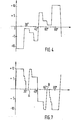
- FIG. 4 shows the "S" curve of the device of FIG. 1, that is to say the characteristic of phase comparator presented by this device.
- Figure 5 shows another distribution of the zones.
- Figure 6 shows another carrier recovery device according to the invention.
- FIG. 7 shows the "S" curve of the device shown in FIG. 6.
- the reference 1 indicates a quadrature detector which supplies signals on wires 1p and 1q from which all the states of a signal d are determined. 'input applied to terminal 2; these signals available on wires 1p and 1q are the projection of the amplitude of the input signal on the components P and 0 in quadrature of a signal supplied by an oscillator 3 provided with a frequency control 4.
- FIG. 2 represents the configuration of these states when the oscillator 3 is considered to be synchronized.
- the modulation of the input signal envisaged is the MAQ16 modulation, that is to say a modulation with 16 states; these states are identified in Figure 2 by E1, E2, E3, ..., E16; the state E1 is characterized by signals of amplitude "1" reported on the components P and Q, the state E3 by signals of amplitude "3” reported on the components P and Q, the state E2 by signals of amplitudes "3" and “1” reported respectively on the components P and Q and the state E4 by signals of amplitudes "1” and "3” reported respectively on the components P and Q.
- the states E5, E6. E7 and E8 occupy symmetrical positions, compared to the component Q in the states E1, E4, E3 and E2.
- means for supplying a correction signal to the frequency control 4 via an integrating low-pass filter 5.
- These means comprise inter alia a circuit for determining zones 10 in the plane P and Q components and according to the invention a weighting circuit 12 at the output of which appears the correction signal dependent, according to variable weights, of different zones defined by the zone determination circuit.
- Different logic circuits will determine different zones from the logic signals provided by these decision circuits.
- Doors “OR EXCLUSIVE" 40, 4 1 and 42 determine zones X represented by the references X1 to X8 in FIG. 3a.
- the door 42 is provided with two inputs, one of which is connected to the output of the door 40 and the other, to the output of the door 41.
- the two inputs of the door 40 are combined at the output of the two decision circuits 19 and 20 and the two inputs of gate 41 at the output of circuits 16 and 18.
- the output signal of gate 42 provides a logic value signal "1" for the hatched areas X2, X4, X6 and X8 and the value "0" for the other zones X1, X3, X5 and X7.
- the "OR" doors 45, 46 and 47 and the "EXCLUSIVE OR” door 48 with inverting output cooperating with the door 42 determine zones Y represented by the references Y1 to Y16 in FIG. 3b.
- the door 48 is provided with a first input which is connected to the outlet of the door 42 and a second one at the outlet of the door 47.
- the door 47 is provided with a first inlet which is connected to the outlet of the door 45 and a second at the exit of door 46; the two inputs of gate 45 are connected respectively to the outputs of decision circuits 30 and 31 and those of gate 46 to the outputs of circuits 32 and 33.
- the output signal of gate 48 provides a signal with logic value "1" for hatched areas Y1, Y4, Y5, Y8, Y9, Y12, Y13 and Y16 and the value "0" for the remaining areas Y2, Y3, Y6, Y7, Y10, Y11, Y14 and Y15.
- the "OR" doors 50, 51 and 52 and the "EXCLUSIVE OR” door 53 cooperating with the door 42 determine zones Z represented by the references Z1 to Z16 in FIG. 3c.
- the door 53 is provided with a first input which is connected to the outlet of the door 42 and a second one at the outlet of the door 52.
- the door 52 is provided with a first inlet which is connected to the outlet of the door 50 and a second at the output of door 51.
- the two inputs of door 50 are respectively connected to the outputs of the circuits decision 34 and 35 and those of gate 51 at the outputs of circuits 36 and 37.
- the output signal of gate 53 provides a logic value signal "1" for the hatched areas Z2, Z3, Z6, Z7, Z10, Z11, Z14 and Z15 and the value "0" for the remaining zones Z1, Z4, Z5, Z8, Z9, Z12, Z13 and Z16.
- the distribution of the zones is determined by successive rotations of the first quadrant around the point of intersection of the lines P and Q.
- the decision circuits can be used to supply logic signals corresponding to the different states E1 to E16. If we call FQ, FP, FQ2; FQ2 ', FP2 and FP2 'the signals at the output of the decision circuits 19, 20, 34, 35, 36 and 37 respectively, a coding circuit 70 supplies signals representing the states E1 to E16.
- the coding circuit 70 performs the following logic operations.
- states can be determined directly by dibits; for example, the first dibit of a state gives the number of the quadrant, this is obtained by the comparators 19 and 20 and the second dibit gives the place of the dibit in the quadrant this is obtained by the comparators 34 to 37 and the doors 50 and 51.
- FIG. 4 the "S" curve, or phase characteristic of the carrier recovery device of FIG. 1, has been represented. On the ordinate, the arbitrary units have been plotted while the abscissa is indicated in degrees . It can be seen that with this device of the invention, we are not confronted with the problems of false clashes.
- the distribution of the zones is deduced by successive rotations of the zones of the first quadrant.
- the device shown in a variant in FIG. 6 realizes the configuration of the zones in FIG. 5.
- This device is formed by a zone determination circuit 10 comprising the elements 15, 16, 17, 18, 19, 20, 34, 35, 36, 37, 40, 41, 42, 50 and 51 already mentioned, a door "OR EXCLUSIVE" 80 whose inputs are connected to the outputs of doors 50 and 51 and whose output is connected to the input of another door "OR EXCLUSIVE" 81, the other input of door 81 is connected to the exit from door 42.
Landscapes
- Engineering & Computer Science (AREA)
- Computer Networks & Wireless Communication (AREA)
- Signal Processing (AREA)
- Digital Transmission Methods That Use Modulated Carrier Waves (AREA)
- Networks Using Active Elements (AREA)
Applications Claiming Priority (2)
| Application Number | Priority Date | Filing Date | Title |
|---|---|---|---|
| FR8303688A FR2542536B1 (fr) | 1983-03-07 | 1983-03-07 | Dispositif de recuperation de la porteuse d'un signal d'entree module par sauts d'amplitude et par sauts de phase |
| FR8303688 | 1983-03-07 |
Publications (2)
| Publication Number | Publication Date |
|---|---|
| EP0118156A1 true EP0118156A1 (de) | 1984-09-12 |
| EP0118156B1 EP0118156B1 (de) | 1986-10-15 |
Family
ID=9286560
Family Applications (1)
| Application Number | Title | Priority Date | Filing Date |
|---|---|---|---|
| EP84200288A Expired EP0118156B1 (de) | 1983-03-07 | 1984-03-01 | Schaltung zur Trägerrückgewinnung für ein in Amplituden- und Phasenstufen moduliertes Signal |
Country Status (9)
| Country | Link |
|---|---|
| US (1) | US4587498A (de) |
| EP (1) | EP0118156B1 (de) |
| JP (1) | JPS59168750A (de) |
| AU (1) | AU558495B2 (de) |
| CA (1) | CA1208712A (de) |
| DE (1) | DE3461013D1 (de) |
| FI (1) | FI82165C (de) |
| FR (1) | FR2542536B1 (de) |
| NO (1) | NO840819L (de) |
Cited By (7)
| Publication number | Priority date | Publication date | Assignee | Title |
|---|---|---|---|---|
| WO1986000940A1 (en) * | 1984-07-20 | 1986-02-13 | Hughes Aircraft Company | Growth of single crystal cadmium-indium-telluride |
| FR2581277A1 (fr) * | 1985-04-30 | 1986-10-31 | Labo Electronique Physique | Circuit de recuperation de l'onde porteuse de systemes de transmissions numeriques |
| EP0224556A4 (de) * | 1985-05-20 | 1989-10-24 | Telebit Corp | Aufbau von ensemblemodems für unvollkommene übertragungsmedien. |
| EP0692896A1 (de) * | 1994-07-12 | 1996-01-17 | Laboratoires D'electronique Philips S.A.S. | Trägerrückwinnung bei QAM |
| FR2722630A1 (fr) * | 1994-07-12 | 1996-01-19 | Philips Electronique Lab | Systeme de transmission numerique comportant un recepteur muni d'un dispositif de recuperation de porteuse |
| FR2733107A1 (fr) * | 1995-04-12 | 1996-10-18 | Philips Electronique Lab | Systeme de transmission numerique de donnees comportant un recepteur synchronise numeriquement |
| EP1940104A3 (de) * | 2006-12-29 | 2012-07-25 | Trident Microsystems (Far East) Ltd. | Vorrichtung und Verfahren zum Entscheiden eines Symbols beim Empfang eines mit einem Quadratursignalpaar gekoppelten Signals zur QAM-Frequenzregelung und/oder Rotationsregelung |
Families Citing this family (16)
| Publication number | Priority date | Publication date | Assignee | Title |
|---|---|---|---|---|
| US4991030A (en) * | 1986-07-07 | 1991-02-05 | Canon Kabushiki Kaisha | Image reading apparatus capable of reading a projected image and having means for diffusing the projected luminous flux |
| US4686689A (en) * | 1986-07-24 | 1987-08-11 | Graham-Patten Systems, Inc. | Phase-locked loop circuit |
| US4712221A (en) * | 1986-08-29 | 1987-12-08 | International Business Machines Corporation | Carrier recovery of modulated signals |
| EP0378719B1 (de) * | 1989-01-18 | 1994-04-27 | Siemens Aktiengesellschaft | Digitaler Verzerrer |
| GB2323505B (en) * | 1994-03-18 | 1998-11-04 | Fujitsu Ltd | Radio receiver for use in the reception of digital multiplexing signals |
| JP2911773B2 (ja) * | 1994-03-18 | 1999-06-23 | 富士通株式会社 | ディジタル多重無線受信装置 |
| US5519733A (en) * | 1994-05-05 | 1996-05-21 | General Instrument Corporation Of Delaware | Method and apparatus for recovering a qam carrier |
| AU739051B2 (en) * | 1996-12-24 | 2001-10-04 | General Dynamics Government Systems Corporation | Symbol lock detector |
| US5987069A (en) * | 1996-12-24 | 1999-11-16 | Gte Government Systems Corporation | Method and apparatus for variably allocating upstream and downstream communication spectra |
| US6304594B1 (en) | 1998-07-27 | 2001-10-16 | General Dynamics Government Systems Corporation | Interference detection and avoidance technique |
| US6560294B1 (en) | 1998-09-25 | 2003-05-06 | Texas Instruments Incorporated | Phase estimation in carrier recovery of phase-modulated signals such as QAM signals |
| US6212229B1 (en) | 1998-12-16 | 2001-04-03 | General Dynamics Government Systems Corporation | Adaptive pre-emphasis technique |
| US6707863B1 (en) | 1999-05-04 | 2004-03-16 | Northrop Grumman Corporation | Baseband signal carrier recovery of a suppressed carrier modulation signal |
| US8000667B2 (en) * | 2006-02-03 | 2011-08-16 | Johnson Controls Technology Company | System and method for compensating for modulation induced frequency shift during transmission of a radio frequency signal |
| US8259859B2 (en) * | 2009-09-21 | 2012-09-04 | Techwell Llc | Method and system for carrier recovery for QAM |
| JP6156807B2 (ja) * | 2013-11-15 | 2017-07-05 | 国立研究開発法人産業技術総合研究所 | 受信信号処理装置、通信システム及び受信信号処理方法 |
Citations (3)
| Publication number | Priority date | Publication date | Assignee | Title |
|---|---|---|---|---|
| US3970946A (en) * | 1973-07-12 | 1976-07-20 | Nippon Electric Company, Ltd. | Demodulator for amplitude-and-phase modulated signals having control means for reducing phase and amplitude errors |
| US4057762A (en) * | 1975-12-26 | 1977-11-08 | Nippon Electric Company, Ltd. | Device for phase synchronizing a reproduced reference carrier signal with windows specified for preselected ones of amplitude and phase modulated signal points |
| DE3030145A1 (de) * | 1979-08-10 | 1981-02-26 | Nippon Electric Co | Phasensynchronisationsschaltkreis fuer die uebertragung von signalen mit mehrstufiger, mehrphasiger ueberlagerungsmodulation |
-
1983
- 1983-03-07 FR FR8303688A patent/FR2542536B1/fr not_active Expired
-
1984
- 1984-03-01 EP EP84200288A patent/EP0118156B1/de not_active Expired
- 1984-03-01 CA CA000448668A patent/CA1208712A/en not_active Expired
- 1984-03-01 DE DE8484200288T patent/DE3461013D1/de not_active Expired
- 1984-03-02 FI FI840842A patent/FI82165C/fi not_active IP Right Cessation
- 1984-03-05 NO NO840819A patent/NO840819L/no unknown
- 1984-03-06 AU AU25301/84A patent/AU558495B2/en not_active Ceased
- 1984-03-07 JP JP59042230A patent/JPS59168750A/ja active Granted
- 1984-03-07 US US06/587,089 patent/US4587498A/en not_active Expired - Fee Related
Patent Citations (3)
| Publication number | Priority date | Publication date | Assignee | Title |
|---|---|---|---|---|
| US3970946A (en) * | 1973-07-12 | 1976-07-20 | Nippon Electric Company, Ltd. | Demodulator for amplitude-and-phase modulated signals having control means for reducing phase and amplitude errors |
| US4057762A (en) * | 1975-12-26 | 1977-11-08 | Nippon Electric Company, Ltd. | Device for phase synchronizing a reproduced reference carrier signal with windows specified for preselected ones of amplitude and phase modulated signal points |
| DE3030145A1 (de) * | 1979-08-10 | 1981-02-26 | Nippon Electric Co | Phasensynchronisationsschaltkreis fuer die uebertragung von signalen mit mehrstufiger, mehrphasiger ueberlagerungsmodulation |
Cited By (10)
| Publication number | Priority date | Publication date | Assignee | Title |
|---|---|---|---|---|
| WO1986000940A1 (en) * | 1984-07-20 | 1986-02-13 | Hughes Aircraft Company | Growth of single crystal cadmium-indium-telluride |
| EP0187843A1 (de) * | 1984-07-20 | 1986-07-23 | Hughes Aircraft Co | Wachstum von einkristallinen cadmium-indium-tellurid. |
| FR2581277A1 (fr) * | 1985-04-30 | 1986-10-31 | Labo Electronique Physique | Circuit de recuperation de l'onde porteuse de systemes de transmissions numeriques |
| EP0200271A1 (de) * | 1985-04-30 | 1986-11-05 | Laboratoires D'electronique Philips | Trägerrückgewinnungsschaltung für digitale Übertragungssysteme |
| EP0224556A4 (de) * | 1985-05-20 | 1989-10-24 | Telebit Corp | Aufbau von ensemblemodems für unvollkommene übertragungsmedien. |
| EP0692896A1 (de) * | 1994-07-12 | 1996-01-17 | Laboratoires D'electronique Philips S.A.S. | Trägerrückwinnung bei QAM |
| FR2722630A1 (fr) * | 1994-07-12 | 1996-01-19 | Philips Electronique Lab | Systeme de transmission numerique comportant un recepteur muni d'un dispositif de recuperation de porteuse |
| US5684842A (en) * | 1994-07-12 | 1997-11-04 | U.S. Philips Corporation | Digital transmission system comprising a receiver which includes a carrier recovery circuit |
| FR2733107A1 (fr) * | 1995-04-12 | 1996-10-18 | Philips Electronique Lab | Systeme de transmission numerique de donnees comportant un recepteur synchronise numeriquement |
| EP1940104A3 (de) * | 2006-12-29 | 2012-07-25 | Trident Microsystems (Far East) Ltd. | Vorrichtung und Verfahren zum Entscheiden eines Symbols beim Empfang eines mit einem Quadratursignalpaar gekoppelten Signals zur QAM-Frequenzregelung und/oder Rotationsregelung |
Also Published As
| Publication number | Publication date |
|---|---|
| JPH0422380B2 (de) | 1992-04-16 |
| JPS59168750A (ja) | 1984-09-22 |
| FI82165C (fi) | 1991-01-10 |
| NO840819L (no) | 1984-09-10 |
| FR2542536B1 (fr) | 1985-07-12 |
| US4587498A (en) | 1986-05-06 |
| FI82165B (fi) | 1990-09-28 |
| FI840842A0 (fi) | 1984-03-02 |
| FI840842A7 (fi) | 1984-09-08 |
| EP0118156B1 (de) | 1986-10-15 |
| AU2530184A (en) | 1984-09-13 |
| AU558495B2 (en) | 1987-01-29 |
| DE3461013D1 (en) | 1986-11-20 |
| CA1208712A (en) | 1986-07-29 |
| FR2542536A1 (fr) | 1984-09-14 |
Similar Documents
| Publication | Publication Date | Title |
|---|---|---|
| EP0118156B1 (de) | Schaltung zur Trägerrückgewinnung für ein in Amplituden- und Phasenstufen moduliertes Signal | |
| DE68908912T2 (de) | Übertragungssystem mit MSK-Modulation und kohärenter differentieller Detektion. | |
| EP0054829B1 (de) | Verfahren und Einrichtung zur Detektion der Trainingsfolge eines autoadaptiven Entzerrers | |
| JP3728573B2 (ja) | 復調装置 | |
| FR2673344A1 (fr) | Comparateur de phase/frequence pour circuit de recuperation de rythme. | |
| EP0125723A1 (de) | Vom Basisband ausgehend gesteuerte Trägerfrequenzentzerrereinrichtung | |
| DE68908038T2 (de) | Frequenzabweichungstolerierendes Verfahren und Vorrichtung zur Demodulation von, durch eine Binärsymbolreihe, winkelmodulierten Signalen mit konstanter Umhüllung und kontinuierlicher Phase. | |
| DE3852454T2 (de) | Empfänger, geeignet für die Verbesserung des Geräuschabstands bei der Wiedergabe digitaler Signale. | |
| CA2109880C (fr) | Dispositif de recuperation du rythme baud dans un recepteur pour modem | |
| EP0630137A1 (de) | Empfangssystem für phasen- und amplitudemodulierte digitale Signale | |
| EP0579100B1 (de) | Verfahren und Einrichtung zur Phasenkorrektur im Basisband eines PSK-Empfängers | |
| FR2466145A1 (fr) | Circuit de synchronisation de phases pour systeme de transmission de signaux modules par superposition a phases multiples, a niveaux multiples | |
| Osborne | A Generalized" Polarity-Type" Costas Loop for Tracking MPSK Signals | |
| US3727134A (en) | Auto equalizer apparatus | |
| CA1052451A (fr) | Ensemble demodulateur pour trains a modulation de phase differentielle | |
| JP3294017B2 (ja) | 複素ベースバンド信号のデジタル発生方法 | |
| FR2505111A1 (fr) | Dispositif de recuperation de porteuse pour une modulation d'amplitude et de phase a seize etats et systeme de reception de donnees numeriques comprenant un tel dispositif | |
| DE69327450T2 (de) | 1-Bit differentiell arbeitender GMSK-Detektor mit Kompensation des Frequenzversatzes | |
| EP1179936A1 (de) | Demodulator für CPFSK-modulierte Signale unter Verwendung einer linearen Näherung des CPFSK-Signals | |
| DE10300267B4 (de) | Demodulation eines frequenzmodulierten Empfangssignals durch Abbilden der Nulldurchgänge auf eine Folge von Parameterwerten | |
| US20040223567A1 (en) | Clock recovery system | |
| DE69909516T2 (de) | Verfahren zum empfangen von spreizspektrumsignalen mit korrektur des frequenzversatzes | |
| Wulich et al. | Synthesis of discrete time-varying null filters for frequency-varying signals using the time-warping technique | |
| EP1530857B1 (de) | Demodulation eines cpfsk-signals mittels berechnung der nulldurchgänge und eines viterbi-algorithmus | |
| Goodwin et al. | Choice of basis functions for continuous and discrete system modelling |
Legal Events
| Date | Code | Title | Description |
|---|---|---|---|
| PUAI | Public reference made under article 153(3) epc to a published international application that has entered the european phase |
Free format text: ORIGINAL CODE: 0009012 |
|
| AK | Designated contracting states |
Designated state(s): BE CH DE FR GB IT LI NL SE |
|
| 17P | Request for examination filed |
Effective date: 19841130 |
|
| GRAA | (expected) grant |
Free format text: ORIGINAL CODE: 0009210 |
|
| AK | Designated contracting states |
Kind code of ref document: B1 Designated state(s): BE CH DE FR GB IT LI NL SE |
|
| REF | Corresponds to: |
Ref document number: 3461013 Country of ref document: DE Date of ref document: 19861120 |
|
| ITF | It: translation for a ep patent filed | ||
| PGFP | Annual fee paid to national office [announced via postgrant information from national office to epo] |
Ref country code: NL Payment date: 19870331 Year of fee payment: 4 |
|
| PLBE | No opposition filed within time limit |
Free format text: ORIGINAL CODE: 0009261 |
|
| STAA | Information on the status of an ep patent application or granted ep patent |
Free format text: STATUS: NO OPPOSITION FILED WITHIN TIME LIMIT |
|
| 26N | No opposition filed | ||
| PG25 | Lapsed in a contracting state [announced via postgrant information from national office to epo] |
Ref country code: LI Effective date: 19890331 Ref country code: CH Effective date: 19890331 |
|
| PG25 | Lapsed in a contracting state [announced via postgrant information from national office to epo] |
Ref country code: NL Effective date: 19891001 |
|
| NLV4 | Nl: lapsed or anulled due to non-payment of the annual fee | ||
| REG | Reference to a national code |
Ref country code: CH Ref legal event code: PL |
|
| REG | Reference to a national code |
Ref country code: FR Ref legal event code: TP |
|
| ITTA | It: last paid annual fee | ||
| ITPR | It: changes in ownership of a european patent |
Owner name: CESSIONE;TRT TELECOMMUNICATIONS RADIOELECTRIQUES E |
|
| REG | Reference to a national code |
Ref country code: GB Ref legal event code: 732E |
|
| EAL | Se: european patent in force in sweden |
Ref document number: 84200288.3 |
|
| PGFP | Annual fee paid to national office [announced via postgrant information from national office to epo] |
Ref country code: BE Payment date: 19960228 Year of fee payment: 13 |
|
| PGFP | Annual fee paid to national office [announced via postgrant information from national office to epo] |
Ref country code: GB Payment date: 19960229 Year of fee payment: 13 |
|
| PGFP | Annual fee paid to national office [announced via postgrant information from national office to epo] |
Ref country code: SE Payment date: 19960326 Year of fee payment: 13 |
|
| PGFP | Annual fee paid to national office [announced via postgrant information from national office to epo] |
Ref country code: FR Payment date: 19960327 Year of fee payment: 13 |
|
| REG | Reference to a national code |
Ref country code: FR Ref legal event code: TP |
|
| PGFP | Annual fee paid to national office [announced via postgrant information from national office to epo] |
Ref country code: DE Payment date: 19960523 Year of fee payment: 13 |
|
| REG | Reference to a national code |
Ref country code: GB Ref legal event code: 732E |
|
| PG25 | Lapsed in a contracting state [announced via postgrant information from national office to epo] |
Ref country code: GB Effective date: 19970301 |
|
| PG25 | Lapsed in a contracting state [announced via postgrant information from national office to epo] |
Ref country code: SE Effective date: 19970302 |
|
| PG25 | Lapsed in a contracting state [announced via postgrant information from national office to epo] |
Ref country code: BE Effective date: 19970331 |
|
| BERE | Be: lapsed |
Owner name: PHILIPS COMMUNICATION D'ENTREPRISE Effective date: 19970331 |
|
| GBPC | Gb: european patent ceased through non-payment of renewal fee |
Effective date: 19970301 |
|
| PG25 | Lapsed in a contracting state [announced via postgrant information from national office to epo] |
Ref country code: FR Free format text: LAPSE BECAUSE OF NON-PAYMENT OF DUE FEES Effective date: 19971128 |
|
| PG25 | Lapsed in a contracting state [announced via postgrant information from national office to epo] |
Ref country code: DE Effective date: 19971202 |
|
| EUG | Se: european patent has lapsed |
Ref document number: 84200288.3 |
|
| REG | Reference to a national code |
Ref country code: FR Ref legal event code: ST |