EP0118199A1 - Appareil pour mesurer la durée de vie du porteur de charge dans un semi-conducteur - Google Patents
Appareil pour mesurer la durée de vie du porteur de charge dans un semi-conducteur Download PDFInfo
- Publication number
- EP0118199A1 EP0118199A1 EP84300626A EP84300626A EP0118199A1 EP 0118199 A1 EP0118199 A1 EP 0118199A1 EP 84300626 A EP84300626 A EP 84300626A EP 84300626 A EP84300626 A EP 84300626A EP 0118199 A1 EP0118199 A1 EP 0118199A1
- Authority
- EP
- European Patent Office
- Prior art keywords
- sample
- beams
- wavelength
- carrier lifetime
- frequency
- Prior art date
- Legal status (The legal status is an assumption and is not a legal conclusion. Google has not performed a legal analysis and makes no representation as to the accuracy of the status listed.)
- Granted
Links
Images



Classifications
-
- H—ELECTRICITY
- H10—SEMICONDUCTOR DEVICES; ELECTRIC SOLID-STATE DEVICES NOT OTHERWISE PROVIDED FOR
- H10P—GENERIC PROCESSES OR APPARATUS FOR THE MANUFACTURE OR TREATMENT OF DEVICES COVERED BY CLASS H10
- H10P74/00—Testing or measuring during manufacture or treatment of wafers, substrates or devices
-
- G—PHYSICS
- G01—MEASURING; TESTING
- G01R—MEASURING ELECTRIC VARIABLES; MEASURING MAGNETIC VARIABLES
- G01R31/00—Arrangements for testing electric properties; Arrangements for locating electric faults; Arrangements for electrical testing characterised by what is being tested not provided for elsewhere
- G01R31/28—Testing of electronic circuits, e.g. by signal tracer
- G01R31/282—Testing of electronic circuits specially adapted for particular applications not provided for elsewhere
- G01R31/2831—Testing of materials or semi-finished products, e.g. semiconductor wafers or substrates
-
- Y—GENERAL TAGGING OF NEW TECHNOLOGICAL DEVELOPMENTS; GENERAL TAGGING OF CROSS-SECTIONAL TECHNOLOGIES SPANNING OVER SEVERAL SECTIONS OF THE IPC; TECHNICAL SUBJECTS COVERED BY FORMER USPC CROSS-REFERENCE ART COLLECTIONS [XRACs] AND DIGESTS
- Y10—TECHNICAL SUBJECTS COVERED BY FORMER USPC
- Y10S—TECHNICAL SUBJECTS COVERED BY FORMER USPC CROSS-REFERENCE ART COLLECTIONS [XRACs] AND DIGESTS
- Y10S136/00—Batteries: thermoelectric and photoelectric
- Y10S136/29—Testing, calibrating, treating, e.g. aging
Definitions
- the present invention relates to a carrier lifetime measuring apparatus which measures minority carrier (current carrier) lifetime within a semiconductor sample on the basis of the frequency dependency of a photovoltage.
- the inventors of the present invention have investigated a carrier lifetime measuring apparatus which measures the minority carrier lifetime within a semiconductor from the bending point of the frequency dependence of a photovoltage.
- This apparatus forms the subject of EP-A-0077021 published after the priority date of the present invention.
- sample e.g. a p-Si wafer having a p-n junction is .
- the apparatus makes it possible to measure the minority carrier lifetime within the sample nondestructively and without forming an electrode on the sample.
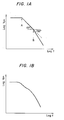
- the photovoltage Vp h is constant at frequencies lower than the cutoff frequency f of the junction. In contrast, it varies proportionally to f -1 for frequencies exceeding f c (point A in Figure 1A of the accompanying drawings), and it varies proportionally to f -3/2 for frequencies exceeding f O (point B in Figure lA).
- the present invention seeks to overcome this problem. It does this by using two light beams, one with a wavelength having a relatively small optical absorption coefficient when incident on the sample and the other having a wavelength having a relatively large optical absorption coefficient. Signals are derived corresponding to the photovoltages generated in the sample by each beam and the ratio used to determine the carrier lifetime. This method eliminates the effects of interface states and traps in the sample, and also may eliminate changes in circuit constants in the measuring system, thereby making possible an accurate determination of carrier lifetime.
- the carrier lifetime may be measured without forming an electrode on the sample, as in the apparatus shown in EP-A-0077021.
- the wavelengths of the light beams depend on the nature of the sample. In general, the beam with the small absorption coefficient will have a longer wavelength than the other beam.
- Z can usually be approximated to an impedance Z j ( ⁇ ) in which a junction resistance R j and a junction capacitance C j are connected in parallel as follows:
- Vph is given by the following equation: In general, ⁇ ⁇ C j R j . It may therefore be expected that, as the frequency is raised, the frequency dependency of V ph is a constant for f ⁇ 1/(27 ⁇ C j R.), V ph ⁇ f -1 for f > 1/(2 ⁇ C j R j ) , and V ph ⁇ f -3/2 for f > 1/(2 ⁇ ).
- Z is not as indicated by Equation (5) when a weak inversion layer or a mere depletion layer exists in an interface or a surface and when interface states or traps or surface states or traps exist in large numbers. Then an impedance Z ss formed by an equivalent resistance R ss and capacitance C ss based on the surface states or traps are connected in series, is incorporated in parallel with Z j as shown in Figure 2B. In consequence, the ⁇ -1 dependence does not occur even for f > f c as shown in Figure 1B, and f o cannot be defined as the frequency corresponding to the transition from an f -1 dependence to an f -3/2 dependence.
- Equation (1) when the frequency dependency of the photocurrent only can be measured, the influence of the surface states or traps appearing in the frequency dependence of Z can be eliminated, and the problem can be solved.
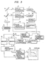
- a first laser 1 oscillates at a wavelength ⁇ 1 of large absorption coefficient ⁇
- a second laser 2 oscillates at a wavelength ⁇ 2 of small absorption coefficient ⁇ .
- the lasers 1 and 2 are powered by a laser power source 13, and selection of laser 1 or laser 2 is achieved by changing-over a switch S1 to side A or side B as appropriate.
- Optical modulators 3 and 4 receive the reference signal of a phase-sensitive demodulator 12 as input signals and respectively chop the radiations of wavelengths ⁇ 1 and ⁇ 2 at a frequency f of the reference signal.
- laser diodes or light emitting diodes are used to form the lasers 1 and 2, their driving currents can be modulated directly, so that the optical modulators 3 and 4 may be omitted and a reduction in the size of the apparatus becomes possible.
- the radiation from the first laser 1 is reflected by a mirror 5.
- a dichroic mirror 6 transmits radiation of wavelength ⁇ 1 reflected from the mirror 5 and reflects radiation of wavelength ⁇ 2 from the second laser 2. With these components, the system is adjusted so that, after light of wavelength ⁇ 1 reflected by the mirror 5 and light of wavelength ⁇ 2 from the optical modulator 4 have come out of the dichroic mirror 6, their optical paths coincide.
- a sample 10 is placed on a sample holder 11 which is made of metal and which serves as an electrode.
- a flat glass plate 8 which is provided with a transparent electrode 9 as an underlying layer is located over the sample 10 with a spacing of at most 100 ⁇ m therebetween.
- the light from the dichroic mirror 6 is focussed onto the sample 10 by a lens 7.
- a photovoltage generated between the electrode 9 and the holder 11 is detected by the phase-sensitive demodulator 12 and is subjected to logarithmic transform by a logarithmic amplifier 14, whereupon the transformed voltage is digitized by an analog-digital converter 15.
- the frequency f of the reference signal of the phase-sensitive demodulator 12 is converted into a voltage 3 signal by an FV (frequency-voltage) converter 16.
- the voltage signal is subjected to logarithmic transform by a logarithmic amplifier 17 and is digitized by an analog-digital converter 18.
- the digital output signal of the A/D converter 18 is stored as frequency information in memories 19 and 20.
- the digital output signal of the A/D converter 15 is stored in the memory 19 or 20 and is changed-over by means of a switch S 2 which interlocks with switch S 1 . That is, when the switches S 1 and S 2 are connected to the A side, data for the wavelength ⁇ 1 is stored in the memory 19, and when they are connected to the B side, data for the wavelength ⁇ 2 is stored in the memory 20.
- the values of Log Vp h and Log f are respectively stored as digital signals in the memories 19 and 20.
- the stored contents are read out from the memories 19 and 20, the difference between Log Vp h for ⁇ 1 and Log V ph for ⁇ 2 is calculated by a signal processing circuit 21.
- the output of the signal processing circuit 21 is converted to an analog signal by digital-analog converter 22, and the analog signal is inputted to the Y-axis of a display unit 24.
- a digital signal having information corresponding to Log f is converted to an analog signal by a digital-analog converter 23, and the analog signal is inputted to'the X-axis of the display unit 24.
- Figure 4 is a block diagram showing a practicable example of the signal processing circuit 21 described above.
- the signal representing the frequency is inputted to the D/A converter 23 via a register 33
- the signal representing the photovoltage corresponding to a light wavelength ⁇ 1 is inputted to a subtractor 34 via a register 31
- the signal representing the photovoltage corresponding to a wavelength ⁇ 2 is inputted to subtractor 34 via a register 32.
- the ratio between the photovoltages derived from the two light sources is calculated by the subtractor 34, and is inputted. to the D/A converter 22.
- Figure 5 shows an example of measurement using such an apparatus.
- the samples were n-type silicon (Si), and each had dimensions of 5 mm x 5 mm x 56 mm.
- Black circles in Figure 5 represent the results at the wavelength ⁇ 2 .
- the characteristic is flat and parallel to the abscissa when the frequency f is not higher than 570 Hz, whereas it is inclined to the abscissa with an inclination proportional to ⁇ -1 ⁇ 2 in a region which exceeds 570 Hz.
- This characteristic demonstrates the frequency dependency of the photocurrent. From this characteristic, the frequency f 0 is determined to be 570 Hz. Thus a value of 280 ⁇ s is obtained for the minority carrier lifetime ⁇ .
- the frequency dependency of a photocurrent included in the frequency dependency of a photovoltage can be measured without being affected by interface states or traps or surface states or traps. This . produces the very significant effect that the absolute value of a minority carrier lifetime can be measured from the frequency of a bending point appearing in the frequency dependency of the photocurrent, irrespective of the type of photovoltage generation such as at a p-n junction or in p-type Si bearing an oxide film.
- a coupling capacitance C m are removed, a measurement of high reliability is possible, and the measurement may be achieved without contacting the sample and nondestructively.
Landscapes
- Engineering & Computer Science (AREA)
- General Engineering & Computer Science (AREA)
- Physics & Mathematics (AREA)
- General Physics & Mathematics (AREA)
- Testing Or Measuring Of Semiconductors Or The Like (AREA)
- Investigating Or Analysing Materials By Optical Means (AREA)
Applications Claiming Priority (2)
| Application Number | Priority Date | Filing Date | Title |
|---|---|---|---|
| JP15174/83 | 1983-02-01 | ||
| JP58015174A JPS59141238A (ja) | 1983-02-01 | 1983-02-01 | キヤリア寿命測定装置 |
Publications (2)
| Publication Number | Publication Date |
|---|---|
| EP0118199A1 true EP0118199A1 (fr) | 1984-09-12 |
| EP0118199B1 EP0118199B1 (fr) | 1986-10-01 |
Family
ID=11881442
Family Applications (1)
| Application Number | Title | Priority Date | Filing Date |
|---|---|---|---|
| EP84300626A Expired EP0118199B1 (fr) | 1983-02-01 | 1984-02-01 | Appareil pour mesurer la durée de vie du porteur de charge dans un semi-conducteur |
Country Status (5)
| Country | Link |
|---|---|
| US (1) | US4581578A (fr) |
| EP (1) | EP0118199B1 (fr) |
| JP (1) | JPS59141238A (fr) |
| CA (1) | CA1203325A (fr) |
| DE (1) | DE3460840D1 (fr) |
Cited By (1)
| Publication number | Priority date | Publication date | Assignee | Title |
|---|---|---|---|---|
| GB2284675A (en) * | 1992-10-19 | 1995-06-14 | Gakuen Ikutoku | Testing electric properties |
Families Citing this family (21)
| Publication number | Priority date | Publication date | Assignee | Title |
|---|---|---|---|---|
| US4706018A (en) * | 1984-11-01 | 1987-11-10 | International Business Machines Corporation | Noncontact dynamic tester for integrated circuits |
| EP0226913A3 (fr) * | 1985-12-17 | 1988-10-05 | Siemens Aktiengesellschaft | Procédé et dispositif pour localiser et/ou afficher des points d'un échantillon conduisant un signal caractéristique dépendant du temps |
| US4786865A (en) * | 1986-03-03 | 1988-11-22 | The Boeing Company | Method and apparatus for testing integrated circuit susceptibility to cosmic rays |
| IT1216540B (it) * | 1988-03-29 | 1990-03-08 | Sgs Thomson Microelectronics | Metodo e apparecchiatura per la misura del tempo di vita su giunzioni p_n a semiconduttore tramite effetto fotovoltaiico. |
| US5025145A (en) * | 1988-08-23 | 1991-06-18 | Lagowski Jacek J | Method and apparatus for determining the minority carrier diffusion length from linear constant photon flux photovoltage measurements |
| JP2889307B2 (ja) * | 1990-03-26 | 1999-05-10 | 株式会社東芝 | ▲iv▼族半導体のキャリアライフタイム測定法 |
| US5053699A (en) * | 1990-05-25 | 1991-10-01 | Texas Instruments Incorporated | Scanning electron microscope based parametric testing method and apparatus |
| JP2702807B2 (ja) * | 1990-08-09 | 1998-01-26 | 東芝セラミックス株式会社 | 半導体中の深い不純物準位の測定方法及びその装置 |
| US5661408A (en) | 1995-03-01 | 1997-08-26 | Qc Solutions, Inc. | Real-time in-line testing of semiconductor wafers |
| US6037797A (en) * | 1997-07-11 | 2000-03-14 | Semiconductor Diagnostics, Inc. | Measurement of the interface trap charge in an oxide semiconductor layer interface |
| US6325078B2 (en) | 1998-01-07 | 2001-12-04 | Qc Solutions, Inc., | Apparatus and method for rapid photo-thermal surface treatment |
| US6154034A (en) * | 1998-10-20 | 2000-11-28 | Lovelady; James N. | Method and apparatus for testing photovoltaic solar cells using multiple pulsed light sources |
| US6512384B1 (en) * | 2000-06-29 | 2003-01-28 | Semiconductor Diagnostics, Inc. | Method for fast and accurate determination of the minority carrier diffusion length from simultaneously measured surface photovoltages |
| US6836139B2 (en) * | 2002-10-22 | 2004-12-28 | Solid State Measurments, Inc. | Method and apparatus for determining defect and impurity concentration in semiconducting material of a semiconductor wafer |
| US6911350B2 (en) * | 2003-03-28 | 2005-06-28 | Qc Solutions, Inc. | Real-time in-line testing of semiconductor wafers |
| US7119569B2 (en) * | 2004-03-05 | 2006-10-10 | Qc Solutions, Inc. | Real-time in-line testing of semiconductor wafers |
| US7200825B2 (en) * | 2004-08-27 | 2007-04-03 | International Business Machines Corporation | Methodology of quantification of transmission probability for minority carrier collection in a semiconductor chip |
| US20070115460A1 (en) * | 2005-11-21 | 2007-05-24 | Capaldo Kevin P | Method for examining molds and apparatus for accomplishing the same |
| US8816715B2 (en) * | 2011-05-12 | 2014-08-26 | Nanya Technology Corp. | MOS test structure, method for forming MOS test structure and method for performing wafer acceptance test |
| RU2484551C1 (ru) * | 2012-01-31 | 2013-06-10 | Закрытое Акционерное Общество "ТЕЛЕКОМ-СТВ" | Способ измерения времени жизни неосновных носителей заряда в кремнии |
| RU2486629C1 (ru) * | 2012-01-31 | 2013-06-27 | Закрытое Акционерное Общество "ТЕЛЕКОМ-СТВ" | Способ контроля времени жизни неосновных носителей заряда в слитках кремния |
Citations (5)
| Publication number | Priority date | Publication date | Assignee | Title |
|---|---|---|---|---|
| US4122383A (en) * | 1977-12-16 | 1978-10-24 | Nasa | Method and apparatus for measuring minority carrier lifetimes and bulk diffusion length in P-N junction solar cells |
| US4211488A (en) * | 1978-10-03 | 1980-07-08 | Rca Corporation | Optical testing of a semiconductor |
| US4273421A (en) * | 1977-01-17 | 1981-06-16 | Motorola, Inc. | Semiconductor lifetime measurement method |
| US4333051A (en) * | 1980-05-28 | 1982-06-01 | Rca Corporation | Method and apparatus for determining minority carrier diffusion length in semiconductors |
| EP0077021A1 (fr) * | 1981-10-09 | 1983-04-20 | Hitachi, Ltd. | Dispositif pour la mesure non-destructive des caractéristiques d'un corps semiconducteur avec une jonction |
Family Cites Families (1)
| Publication number | Priority date | Publication date | Assignee | Title |
|---|---|---|---|---|
| JPS5266373A (en) * | 1975-11-28 | 1977-06-01 | Sharp Corp | Determination of lifetime and surface recombination speed of semicondu ctor device |
-
1983
- 1983-02-01 JP JP58015174A patent/JPS59141238A/ja active Pending
-
1984
- 1984-01-31 US US06/575,691 patent/US4581578A/en not_active Expired - Lifetime
- 1984-01-31 CA CA000446381A patent/CA1203325A/fr not_active Expired
- 1984-02-01 DE DE8484300626T patent/DE3460840D1/de not_active Expired
- 1984-02-01 EP EP84300626A patent/EP0118199B1/fr not_active Expired
Patent Citations (5)
| Publication number | Priority date | Publication date | Assignee | Title |
|---|---|---|---|---|
| US4273421A (en) * | 1977-01-17 | 1981-06-16 | Motorola, Inc. | Semiconductor lifetime measurement method |
| US4122383A (en) * | 1977-12-16 | 1978-10-24 | Nasa | Method and apparatus for measuring minority carrier lifetimes and bulk diffusion length in P-N junction solar cells |
| US4211488A (en) * | 1978-10-03 | 1980-07-08 | Rca Corporation | Optical testing of a semiconductor |
| US4333051A (en) * | 1980-05-28 | 1982-06-01 | Rca Corporation | Method and apparatus for determining minority carrier diffusion length in semiconductors |
| EP0077021A1 (fr) * | 1981-10-09 | 1983-04-20 | Hitachi, Ltd. | Dispositif pour la mesure non-destructive des caractéristiques d'un corps semiconducteur avec une jonction |
Cited By (2)
| Publication number | Priority date | Publication date | Assignee | Title |
|---|---|---|---|---|
| GB2284675A (en) * | 1992-10-19 | 1995-06-14 | Gakuen Ikutoku | Testing electric properties |
| GB2284675B (en) * | 1992-10-19 | 1997-11-12 | Gakuen Ikutoku | Method of evaluating lifetime of semiconductor material and apparatus for the same |
Also Published As
| Publication number | Publication date |
|---|---|
| EP0118199B1 (fr) | 1986-10-01 |
| JPS59141238A (ja) | 1984-08-13 |
| DE3460840D1 (en) | 1986-11-06 |
| CA1203325A (fr) | 1986-04-15 |
| US4581578A (en) | 1986-04-08 |
Similar Documents
| Publication | Publication Date | Title |
|---|---|---|
| EP0118199B1 (fr) | Appareil pour mesurer la durée de vie du porteur de charge dans un semi-conducteur | |
| US4949034A (en) | Method for contactless evaluation of characteristics of semiconductor wafers and devices | |
| US4011016A (en) | Semiconductor radiation wavelength detector | |
| US4464627A (en) | Device for measuring semiconductor characteristics | |
| US4393348A (en) | Method and apparatus for determining minority carrier diffusion length in semiconductors | |
| US4433288A (en) | Method and apparatus for determining minority carrier diffusion length in semiconductors | |
| JPH08316276A (ja) | 電荷測定装置 | |
| JPH02119236A (ja) | 直線状定フォトン束光電圧測定値から少数担体拡散長を判定するための方法および装置 | |
| US3850508A (en) | Method and apparatus for testing the doping concentration of semiconductors | |
| JPH0697210B2 (ja) | スキャナの校正方法及び所定の散乱光振幅の発生装置 | |
| JPS61108148A (ja) | 集積回路製造時の中間体の動的テスト装置 | |
| CN103543130B (zh) | 一种消除光载流子辐射技术半导体材料特性测量装置的系统频率响应影响的方法 | |
| UST102104I4 (en) | Scanning optical system adapted for linewidth measurement in semiconductor devices | |
| EP0274508B1 (fr) | Microscopes | |
| US5010294A (en) | Method for topically-resolved determination of the diffusion length of minority charge carriers in a semiconductor crystal body with the assistance of an electrolytic cell | |
| JP3730289B2 (ja) | 半導体ウェーハの欠陥測定方法及び同装置 | |
| US4642565A (en) | Method to determine the crystalline properties of an interface of two materials by photovoltage phenomenon | |
| JPS6242537Y2 (fr) | ||
| JPS6237531B2 (fr) | ||
| RU2019890C1 (ru) | Способ определения электрофизических параметров неравновесных носителей заряда в подложках диодных структур | |
| JP3258465B2 (ja) | 物理化学センサ | |
| JPS58108752A (ja) | 半導体特性測定装置 | |
| JPH05226445A (ja) | 非接触キャリア拡散長測定装置 | |
| RU2080689C1 (ru) | Устройство для определения электрофизических характеристик полупроводниковых пластин | |
| JPH06112290A (ja) | 半導体評価装置 |
Legal Events
| Date | Code | Title | Description |
|---|---|---|---|
| PUAI | Public reference made under article 153(3) epc to a published international application that has entered the european phase |
Free format text: ORIGINAL CODE: 0009012 |
|
| 17P | Request for examination filed |
Effective date: 19840322 |
|
| AK | Designated contracting states |
Designated state(s): DE FR GB NL |
|
| GRAA | (expected) grant |
Free format text: ORIGINAL CODE: 0009210 |
|
| AK | Designated contracting states |
Kind code of ref document: B1 Designated state(s): DE FR GB NL |
|
| REF | Corresponds to: |
Ref document number: 3460840 Country of ref document: DE Date of ref document: 19861106 |
|
| ET | Fr: translation filed | ||
| PLBE | No opposition filed within time limit |
Free format text: ORIGINAL CODE: 0009261 |
|
| STAA | Information on the status of an ep patent application or granted ep patent |
Free format text: STATUS: NO OPPOSITION FILED WITHIN TIME LIMIT |
|
| 26N | No opposition filed | ||
| PGFP | Annual fee paid to national office [announced via postgrant information from national office to epo] |
Ref country code: GB Payment date: 19970122 Year of fee payment: 14 |
|
| PGFP | Annual fee paid to national office [announced via postgrant information from national office to epo] |
Ref country code: FR Payment date: 19970217 Year of fee payment: 14 |
|
| PGFP | Annual fee paid to national office [announced via postgrant information from national office to epo] |
Ref country code: NL Payment date: 19970228 Year of fee payment: 14 |
|
| PGFP | Annual fee paid to national office [announced via postgrant information from national office to epo] |
Ref country code: DE Payment date: 19970428 Year of fee payment: 14 |
|
| PG25 | Lapsed in a contracting state [announced via postgrant information from national office to epo] |
Ref country code: GB Free format text: LAPSE BECAUSE OF NON-PAYMENT OF DUE FEES Effective date: 19980201 |
|
| PG25 | Lapsed in a contracting state [announced via postgrant information from national office to epo] |
Ref country code: FR Free format text: THE PATENT HAS BEEN ANNULLED BY A DECISION OF A NATIONAL AUTHORITY Effective date: 19980228 |
|
| PG25 | Lapsed in a contracting state [announced via postgrant information from national office to epo] |
Ref country code: NL Free format text: LAPSE BECAUSE OF NON-PAYMENT OF DUE FEES Effective date: 19980901 |
|
| GBPC | Gb: european patent ceased through non-payment of renewal fee |
Effective date: 19980201 |
|
| NLV4 | Nl: lapsed or anulled due to non-payment of the annual fee |
Effective date: 19980901 |
|
| PG25 | Lapsed in a contracting state [announced via postgrant information from national office to epo] |
Ref country code: DE Free format text: LAPSE BECAUSE OF NON-PAYMENT OF DUE FEES Effective date: 19981103 |
|
| REG | Reference to a national code |
Ref country code: FR Ref legal event code: ST |