EP0118368A2 - Registre de participation pour systèmes de test automatiques - Google Patents
Registre de participation pour systèmes de test automatiques Download PDFInfo
- Publication number
- EP0118368A2 EP0118368A2 EP84400449A EP84400449A EP0118368A2 EP 0118368 A2 EP0118368 A2 EP 0118368A2 EP 84400449 A EP84400449 A EP 84400449A EP 84400449 A EP84400449 A EP 84400449A EP 0118368 A2 EP0118368 A2 EP 0118368A2
- Authority
- EP
- European Patent Office
- Prior art keywords
- pin
- data
- registers
- register
- participate
- Prior art date
- Legal status (The legal status is an assumption and is not a legal conclusion. Google has not performed a legal analysis and makes no representation as to the accuracy of the status listed.)
- Granted
Links
Images
Classifications
-
- G—PHYSICS
- G01—MEASURING; TESTING
- G01R—MEASURING ELECTRIC VARIABLES; MEASURING MAGNETIC VARIABLES
- G01R31/00—Arrangements for testing electric properties; Arrangements for locating electric faults; Arrangements for electrical testing characterised by what is being tested not provided for elsewhere
- G01R31/28—Testing of electronic circuits, e.g. by signal tracer
- G01R31/317—Testing of digital circuits
- G01R31/3181—Functional testing
- G01R31/319—Tester hardware, i.e. output processing circuits
- G01R31/31903—Tester hardware, i.e. output processing circuits tester configuration
- G01R31/31908—Tester set-up, e.g. configuring the tester to the device under test [DUT], down loading test patterns
Definitions
- This invention relates to automatic test systems for testing electronic components, and in particular, to a participate register for parallel loading of data in pin oriented registers in automatic test equipment.
- pin electronics interface circuits are coupled to the pins or other nodes of an electronic device being tested.
- stimuli signals are supplied to the device under test, and output signals from the device under test are detected and measured.
- the stimuli signals represent logic states or analog voltages or currents which are desired to be impressed on the pins of the device under test as a parallel pattern, with the resulting output signals checked in parallel.
- the interface circuits function as an interface between the computer controlling the test system and the individual pins of the device under test.
- the interface circuits receive reference voltages and digital data from other circuits in the test system, and then through drivers associated with each interface circuit switch these voltages or data onto desired input pins of the device under test under control of a program stored in the test system computer.
- the interface circuits receive voltages or data from output pins of the device under test and supply that data to a comparator circuit which compares the signal received with the proper response stored in the program of the test system computer.
- each register associated with each pin of the device being tested stores information concerning attributes to be - controlled by those registers.
- a relay register associated with each pin stores information to control the state of relays associated with the pin.
- Other registers associated with each pin store information concerning reference levels, pin modes of operation, connection of a precision analog measurement unit, etc.
- each register associated with each-pin was sequentially addressed and the desired data supplied. Because many of the pin registers received identical data, loading this data into registers required long sets of repetitive instructions thereby causing a lengthy set-up period during which the automatic'test equipment was unavailable for testing electronic components .
- This invention provides an apparatus for an automatic test system by which individual registers associated with different pins, but which are to receive the same data, may be selected and enabled as a group to simultaneously receive that data. In this manner the sequential addressing of individual registers required by the prior art is eliminated except for those data transfers where only one register is to receive the information.
- the parallel loading of groups of registers with common data greatly decreases the set-up time required by the test system.
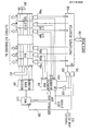
- the Figure is a block diagram illustrating an automatic test system with participate register of the preferred embodiment of this invention.
- the Figure is a schematic drawing illustrating the preferred embodiment of this invention.
- the registers in each column control features associated with the corresponding pin.
- the registers in column 2 will control circuits, relays, or other functions associated with pin 2 of a test fixture into which the device being tested is placed.
- Those registers in column n will control aspects of the operation of circuits coupled to pin n.
- the number of columns of pin registers is arbitrary and may be expanded or reduced depending upon the characteristics of the device being tested. For example, for a 16 pin integrated circuit, typically only pins 0 through 15 of the test fixture will be used, and consequently only pin registers in columns 0 through 15 of register set 100 will be used.
- Each pin of the device being tested will usually have associated with it several pin registers that control different aspects of the signals supplied to or received from the device being tested. For example, in one automatic test system, for each pin a first register will be provided to control the-relays associated with that pin, another register will control the connection of an analog precision measurement unit to the pin, two registers will control the pin mode of operation, and nine registers will allow setting of reference voltage and current levels for the pin.
- the relays, precision measurement units, pin modes of operation, reference levels and other parameters associated with each pin are controlled by the data stored in the particular pin registers corresponding to that individual pin.
- a participate register 150 is provided and connected to address decoder 110 through AND gate 160.
- the participate register 150 is also coupled to data bus 130, the data strobe gate 170, and to each of OR gates 140 as shown.
- the participate register 150 functions as a rank oriented register which, in conjunction with register type decoder 180, controls which pin registers 100 will take part in a given parallel load of data from bus 130. All pin registers selected will then receive information in a single parallel loading operation.
- the operation of the circuit shown in the Figure is as follows. To write data into the participate register 150, it is addressed by address bus 120 through pin address decoder 110 by the selection of a nonexistent pin register address such as A13C. This signal is supplied to the upper terminal of AND gate 160. The other terminal of gate 160 is coupled to the data strobe line, and at the next data strobe signal, data are supplied to participate register 150 from data bus 130.
- the participate register will comprise an n bit register.
- the hypothetical word shown in the Figure loaded into register 150 from data bus 130 is 011...010 as shown.
- register 150 When the output of the participate register 150 is enabled using a selected, address bit supplied on parallel load select line 165, the contents of register 150 will enable selected ones of OR gates 140. For example, if a "1" is considered to enable an OR gate, then OR gates 140b, 140c, and 140n-1 will be enabled simultaneously. These gates, in turn, will enable pin registers designated 1, 2, and 140n-1 to receive data simultaneously from data bus 130.
- Multiplexer 175 and register type decoder 180 in response to signals from bus 120, will select one of rows 101, 102, etc. of pin registers to have selected registers enabled within it.
- the same address bit 165 which, through gate 170, enables the output of the participate register 150 also controls multiplexer 175.
- Multiplexer 175 receives addresses from address bus 120 as shown.
- the addresses supplied to decoder 180 through multiplexer 175 will be decoded to specify the type of register, e.g. relay registers 102, to take part in the parallel loading of data from bus 130. Thus only those of registers 102 also selected by the participate register 150 will receive data from bus 130.
- Inverter 115 coupled to the output enable terminal OE of decoder 110 will disable decoder 110 when the output of participate register 150 is enabled. In this manner the group of pin registers selected by both register 150 and decoder 180 (e.g. Row 102 for pins 1, 2, and n-1) may be loaded in parallel, rather than serially, as in the prior art.
- Parallel loading of data is particularly advantageous in the loading of data in automatic test systems because groups of pin registers often receive the same data to enable them to participate in the same measurement, specify the same relay combination, or perform other functions.
- groups of pin registers often receive the same data to enable them to participate in the same measurement, specify the same relay combination, or perform other functions.
- many participate registers may be provided as desired with each having its own separate address. For example, one participate register may be provided to control one set of pin registers, and a second separate participate register provided to control other features.
Landscapes
- Engineering & Computer Science (AREA)
- General Engineering & Computer Science (AREA)
- Physics & Mathematics (AREA)
- General Physics & Mathematics (AREA)
- Tests Of Electronic Circuits (AREA)
- Testing Relating To Insulation (AREA)
Applications Claiming Priority (2)
| Application Number | Priority Date | Filing Date | Title |
|---|---|---|---|
| US472427 | 1983-03-07 | ||
| US06/472,427 US4594544A (en) | 1983-03-07 | 1983-03-07 | Participate register for parallel loading pin-oriented registers in test equipment |
Publications (3)
| Publication Number | Publication Date |
|---|---|
| EP0118368A2 true EP0118368A2 (fr) | 1984-09-12 |
| EP0118368A3 EP0118368A3 (en) | 1988-03-16 |
| EP0118368B1 EP0118368B1 (fr) | 1992-01-02 |
Family
ID=23875465
Family Applications (1)
| Application Number | Title | Priority Date | Filing Date |
|---|---|---|---|
| EP84400449A Expired EP0118368B1 (fr) | 1983-03-07 | 1984-03-07 | Registre de participation pour systèmes de test automatiques |
Country Status (5)
| Country | Link |
|---|---|
| US (1) | US4594544A (fr) |
| EP (1) | EP0118368B1 (fr) |
| JP (1) | JPH0646213B2 (fr) |
| CA (1) | CA1217232A (fr) |
| DE (1) | DE3485395D1 (fr) |
Families Citing this family (13)
| Publication number | Priority date | Publication date | Assignee | Title |
|---|---|---|---|---|
| JPS6140574A (ja) * | 1984-07-31 | 1986-02-26 | Advantest Corp | 試験条件設定装置 |
| US4766593A (en) * | 1986-12-22 | 1988-08-23 | Motorola, Inc. | Monolithically integrated testable registers that cannot be directly addressed |
| US4856001A (en) * | 1987-05-29 | 1989-08-08 | Zehntel, Inc. | Digital in-circuit tester having channel-memory earse-preventer |
| US4897842A (en) * | 1987-11-05 | 1990-01-30 | Ampex Corporation | Integrated circuit signature analyzer for testing digital circuitry |
| US4947395A (en) * | 1989-02-10 | 1990-08-07 | Ncr Corporation | Bus executed scan testing method and apparatus |
| US5369593A (en) * | 1989-05-31 | 1994-11-29 | Synopsys Inc. | System for and method of connecting a hardware modeling element to a hardware modeling system |
| US5353243A (en) * | 1989-05-31 | 1994-10-04 | Synopsys Inc. | Hardware modeling system and method of use |
| US5225772A (en) * | 1990-09-05 | 1993-07-06 | Schlumberger Technologies, Inc. | Automatic test equipment system using pin slice architecture |
| US5321701A (en) * | 1990-12-06 | 1994-06-14 | Teradyne, Inc. | Method and apparatus for a minimal memory in-circuit digital tester |
| US5673295A (en) * | 1995-04-13 | 1997-09-30 | Synopsis, Incorporated | Method and apparatus for generating and synchronizing a plurality of digital signals |
| US7765443B1 (en) | 2001-03-19 | 2010-07-27 | Credence Systems Corporation | Test systems and methods for integrated circuit devices |
| US7017091B2 (en) * | 2001-03-19 | 2006-03-21 | Credence Systems Corporation | Test system formatters configurable for multiple data rates |
| US7127652B2 (en) * | 2003-06-03 | 2006-10-24 | Agilent Technologies, Inc. | X-tree test method and apparatus in a multiplexed digital system |
Family Cites Families (2)
| Publication number | Priority date | Publication date | Assignee | Title |
|---|---|---|---|---|
| US3651315A (en) * | 1970-05-14 | 1972-03-21 | Collins Radio Co | Digital products inspection system |
| US4212075A (en) * | 1978-10-10 | 1980-07-08 | Usm Corporation | Electrical component testing system for component insertion machine |
-
1983
- 1983-03-07 US US06/472,427 patent/US4594544A/en not_active Expired - Lifetime
-
1984
- 1984-03-06 CA CA000448894A patent/CA1217232A/fr not_active Expired
- 1984-03-06 JP JP59041473A patent/JPH0646213B2/ja not_active Expired - Lifetime
- 1984-03-07 EP EP84400449A patent/EP0118368B1/fr not_active Expired
- 1984-03-07 DE DE8484400449T patent/DE3485395D1/de not_active Expired - Fee Related
Also Published As
| Publication number | Publication date |
|---|---|
| CA1217232A (fr) | 1987-01-27 |
| JPS59230177A (ja) | 1984-12-24 |
| DE3485395D1 (de) | 1992-02-13 |
| EP0118368A3 (en) | 1988-03-16 |
| JPH0646213B2 (ja) | 1994-06-15 |
| US4594544A (en) | 1986-06-10 |
| EP0118368B1 (fr) | 1992-01-02 |
Similar Documents
| Publication | Publication Date | Title |
|---|---|---|
| US6195772B1 (en) | Electronic circuit testing methods and apparatus | |
| US6028439A (en) | Modular integrated circuit tester with distributed synchronization and control | |
| US4724378A (en) | Calibrated automatic test system | |
| US5951705A (en) | Integrated circuit tester having pattern generator controlled data bus | |
| EP0053665B1 (fr) | Test des arrangements incorporés en circuits intégrés à grande échelle | |
| US5444390A (en) | Means and method for sequentially testing electrical components | |
| US4196386A (en) | Method and portable apparatus for testing digital printed circuit boards | |
| US4594544A (en) | Participate register for parallel loading pin-oriented registers in test equipment | |
| EP0491290A2 (fr) | Testeur de circuit intégré | |
| US5053698A (en) | Test device and method for testing electronic device and semiconductor device having the test device | |
| JPS6338728B2 (fr) | ||
| US5835506A (en) | Single pass doublet mode integrated circuit tester | |
| EP0222084A2 (fr) | Système de test à architecture hiérarchique | |
| EP0228332B1 (fr) | Système automatique de test ayant une architecture à "vrai testeur-par-broche" | |
| KR850003007A (ko) | 데이타 처리 시스템의 시험 및 보수 방법과 장치 | |
| KR0138258B1 (ko) | 고속 집적 회로의 테스팅 방법 및 테스팅 장치 | |
| US6781398B2 (en) | Circuit for testing an integrated circuit | |
| KR960003363B1 (ko) | Ic 시험장치 | |
| JP3090785B2 (ja) | 直流レベル発生装置 | |
| US5459738A (en) | Apparatus and method for digital circuit testing | |
| JP3145283B2 (ja) | Ic試験装置のレジスタデータ書込み方式 | |
| JP3210236B2 (ja) | Ic試験装置のパターン発生装置 | |
| JPS60120269A (ja) | 半導体テスト装置 | |
| JP2659043B2 (ja) | 電気部品試験機のチャネル制御装置 | |
| JPH05307900A (ja) | 半導体メモリ素子 |
Legal Events
| Date | Code | Title | Description |
|---|---|---|---|
| PUAI | Public reference made under article 153(3) epc to a published international application that has entered the european phase |
Free format text: ORIGINAL CODE: 0009012 |
|
| AK | Designated contracting states |
Designated state(s): DE FR GB IT NL |
|
| PUAL | Search report despatched |
Free format text: ORIGINAL CODE: 0009013 |
|
| AK | Designated contracting states |
Kind code of ref document: A3 Designated state(s): DE FR GB IT NL |
|
| 17P | Request for examination filed |
Effective date: 19880816 |
|
| 17Q | First examination report despatched |
Effective date: 19891012 |
|
| RAP1 | Party data changed (applicant data changed or rights of an application transferred) |
Owner name: FAIRCHILD SEMICONDUCTOR CORPORATION |
|
| RAP1 | Party data changed (applicant data changed or rights of an application transferred) |
Owner name: SCHLUMBERGER TECHNOLOGIES, INC. |
|
| GRAA | (expected) grant |
Free format text: ORIGINAL CODE: 0009210 |
|
| AK | Designated contracting states |
Kind code of ref document: B1 Designated state(s): DE FR GB IT NL |
|
| PG25 | Lapsed in a contracting state [announced via postgrant information from national office to epo] |
Ref country code: NL Effective date: 19920102 Ref country code: IT Free format text: LAPSE BECAUSE OF FAILURE TO SUBMIT A TRANSLATION OF THE DESCRIPTION OR TO PAY THE FEE WITHIN THE PRESCRIBED TIME-LIMIT;WARNING: LAPSES OF ITALIAN PATENTS WITH EFFECTIVE DATE BEFORE 2007 MAY HAVE OCCURRED AT ANY TIME BEFORE 2007. THE CORRECT EFFECTIVE DATE MAY BE DIFFERENT FROM THE ONE RECORDED. Effective date: 19920102 |
|
| REF | Corresponds to: |
Ref document number: 3485395 Country of ref document: DE Date of ref document: 19920213 |
|
| ET | Fr: translation filed | ||
| NLV1 | Nl: lapsed or annulled due to failure to fulfill the requirements of art. 29p and 29m of the patents act | ||
| PLBE | No opposition filed within time limit |
Free format text: ORIGINAL CODE: 0009261 |
|
| STAA | Information on the status of an ep patent application or granted ep patent |
Free format text: STATUS: NO OPPOSITION FILED WITHIN TIME LIMIT |
|
| 26N | No opposition filed | ||
| REG | Reference to a national code |
Ref country code: GB Ref legal event code: IF02 |
|
| PGFP | Annual fee paid to national office [announced via postgrant information from national office to epo] |
Ref country code: GB Payment date: 20020306 Year of fee payment: 19 |
|
| PGFP | Annual fee paid to national office [announced via postgrant information from national office to epo] |
Ref country code: FR Payment date: 20020312 Year of fee payment: 19 |
|
| PGFP | Annual fee paid to national office [announced via postgrant information from national office to epo] |
Ref country code: DE Payment date: 20020320 Year of fee payment: 19 |
|
| PG25 | Lapsed in a contracting state [announced via postgrant information from national office to epo] |
Ref country code: GB Free format text: LAPSE BECAUSE OF NON-PAYMENT OF DUE FEES Effective date: 20030307 |
|
| PG25 | Lapsed in a contracting state [announced via postgrant information from national office to epo] |
Ref country code: DE Free format text: LAPSE BECAUSE OF NON-PAYMENT OF DUE FEES Effective date: 20031001 |
|
| GBPC | Gb: european patent ceased through non-payment of renewal fee |
Effective date: 20030307 |
|
| PG25 | Lapsed in a contracting state [announced via postgrant information from national office to epo] |
Ref country code: FR Free format text: LAPSE BECAUSE OF NON-PAYMENT OF DUE FEES Effective date: 20031127 |
|
| REG | Reference to a national code |
Ref country code: FR Ref legal event code: ST |