EP0118762A2 - Dispositif de conversion numérique-analogique - Google Patents
Dispositif de conversion numérique-analogique Download PDFInfo
- Publication number
- EP0118762A2 EP0118762A2 EP84101289A EP84101289A EP0118762A2 EP 0118762 A2 EP0118762 A2 EP 0118762A2 EP 84101289 A EP84101289 A EP 84101289A EP 84101289 A EP84101289 A EP 84101289A EP 0118762 A2 EP0118762 A2 EP 0118762A2
- Authority
- EP
- European Patent Office
- Prior art keywords
- signal
- frequency
- digital
- sampling
- signals
- Prior art date
- Legal status (The legal status is an assumption and is not a legal conclusion. Google has not performed a legal analysis and makes no representation as to the accuracy of the status listed.)
- Withdrawn
Links
Images



Classifications
-
- H—ELECTRICITY
- H04—ELECTRIC COMMUNICATION TECHNIQUE
- H04B—TRANSMISSION
- H04B14/00—Transmission systems not characterised by the medium used for transmission
- H04B14/02—Transmission systems not characterised by the medium used for transmission characterised by the use of pulse modulation
- H04B14/04—Transmission systems not characterised by the medium used for transmission characterised by the use of pulse modulation using pulse code modulation
-
- H—ELECTRICITY
- H03—ELECTRONIC CIRCUITRY
- H03M—CODING; DECODING; CODE CONVERSION IN GENERAL
- H03M1/00—Analogue/digital conversion; Digital/analogue conversion
- H03M1/06—Continuously compensating for, or preventing, undesired influence of physical parameters
- H03M1/0617—Continuously compensating for, or preventing, undesired influence of physical parameters characterised by the use of methods or means not specific to a particular type of detrimental influence
- H03M1/0626—Continuously compensating for, or preventing, undesired influence of physical parameters characterised by the use of methods or means not specific to a particular type of detrimental influence by filtering
- H03M1/0631—Smoothing
Definitions
- This invention generally relates to PCM (Pulse Code Modulation) systems and more particularly to a digital-to-analog converter device suitable for a PCM system wherein PCM signals at different sampling frequencies are converted into analog signals.
- PCM Pulse Code Modulation
- a prior art digital-to-analog converter circuit will be described with reference to a schematic construction diagram as shown in Fig. 1 and a characteristic diagram as shown in Fig. 2.
- a PCM signal 1 is converted into an analog signal 3 by means of a digital-to-analog converter (DAC) 2.
- DAC digital-to-analog converter
- the analog signal 3 is filtered by a low-pass filter 4 to produce an output signal 5.
- the low-pass filter 4 used herein will be described in greater detail with reference to Fig. 2.
- a spectrum of the analog signal 3 is exemplified at section (a) in Fig. 2, where f s designates a sampling frequency. While the signal spectrum covers frequencies ranging from 0 (zero) to f s /2, a side band component for the sampling frequency f s ranges from f s -f s /2 to f s + f s /2. Since the output signal must be removed of the side band component, the low-pass filter is needed.
- the low-pass filter thus requires a characteristic as exemplified at (b) in Fig. 2 and with this filter, an output signal as shown at (c) in Fig. 2 can be obtained.
- the filter Practically, however, it is difficult for the filter to have such an abrupt attenuation characteristic and hence the signal frequency band is set to below half the sampling frequency f s , for example, to 20 KHz in the case of a so-called compact disc wherein the sampling frequency is 44.1 KHz, and the filter is designed to have a pass band cut-off frequency f of 20 KHz as shown at (d) in Fig. 2.
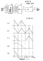
- a construction as shown in Fig. 3 is known as adapted to simplify the low-pass filter using a digital filter, from for example, Japanese literatures, Yamasaki et al "Application of Real Time Convolution for Audio Equipments” in papers of Acoustical Society of Japan, Oct. 1978, pp 247-248 and Yamasaki et al "PCM Digital Audio” published by Seibundo Shinkosha, Nov. 1980, pp 121 - 124.
- a PCM signal 1 used in for example, a space sattelite broadcasting system is subjected to conversion of its sampling frequency f and band filtering by means of a signal converter 6.
- An output signal 7 from the signal converter 6 is converted into an analog signal 3 by means of a digital-to-analog converter 2.
- the analog signal 3 is filtered at a low-pass filter 4 to produce an output signal 5.
- the audio broadcast mode A has an audio signal transmission band of 15 KHz, a sampling frequency of 32 KHz and a quantization and compander rate of 14/10 bits and the B mode has 20 KHz, 48 KHz and 16 bits.
- the PCM signal 1 has a frequency spectrum as shown at section (a) in Fig. 4.
- a signal component covering a frequency band f s /2 is sampled at a sampling frequency f s .
- the sampling frequency of this signal e.g., 32 KHz is converted into f s ' e.g., 64 KHz, providing a frequency spectrum as shown at (b) in Fig. 4.
- Signal components above the f s /2 band are subjected to low-pass filtering by means of the digital filter 6, providing a frequency spectrum as shown at (c) in Fig. 4.
- the output signal 7 of the digital filter 6 has therefore this frequency spectrum.
- the output signal 7 is converted into the analog signal by the digital-to-analog converter 2 and passed through the filter 4 having a low-pass characteristic as shown at (d) in Fig. 4, thus providing a characteristic as shown at (e) in Fig. 4.
- the digital-to-analog converter 2 must be so designed as to respond to the sampling frequency fs
- the ramped band cut-off characteristic of the low-pass filter 4 becomes more gradual as the sampling frequency f s ' increases with respect to the sampling frequency f s .
- a PCM signal at a single standard frequency is not employed but one PCM signal covering a 15 KHz band which is sampled at a sampling frequency 32 KHz for 4-channel sounds and the other PCM signal covering a 20 KHz band which is sampled at a sampling frequency 48 KHz for 2-channel sounds are switched on time series so as to be broadcast.
- separate low-pass filters adapted for the respective PCM signals must be prepared if the prior art technical idea is applied by itself.
- An object of this invention is to provide a digital-to-analog converter device with a single low-pass filter which can ensure low-pass filtering for a plurality of PCM signals at different sampling frequencies which are received on time series.
- a signal converter which expands the frequency distance between a PCM signal band and a side band by converting at least one of different sampling frequencies into a predetermined frequency e.g., a higher frequency.
- a low-pass filter can be simplified, having a gradual ramp cut-off characteristic for removal of the side band wherein a pass band cut-off frequency and a stop band cut-off frequency can be adapted for low-pass filtering of the plurality of PCM signals at different sampling frequencies.
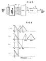
- FIG. 5 one embodiment of a digital-to-analog converter device according to this invention is schematically shown in block form.
- PCM signals at sampling frequencies f s1 and f s2 have frequency spectra as shown at section (a) in Fig. 6. These two PCM signals as designated at reference numeral 1 are supplied to a signal converter 6a of Fig. 5 on time series.
- the common low-pass filter 4a has a pass band cut-off frequency f cl of 20 KHz and a stop band cut-off frequency f c2 of 49 KHz. Therefore, in response to one PCM signal associated with the sampling frequency f sl , a desired output signal of dotted line as shown at (d) in Fig. 6 can be obtained and for the other PCM signal at the sampling frequency fs2, a desired output signal of solid line as shown at Fig. 6(d) can be obtained.
- this converter fulfils a duplex function including the conversion of the sampling frequencies for the input PCM signals into higher frequencies and the low-pass filtering of the signal bands as has been described previously with reference to Fig. 6.
- a digital filter may be used.
- the input sampled data is used when sampling points after the conversion coincide with sampling points of the data but when the coincidence disappears, intermediate points in time between the sampling points after the conversion are added with zero.
- PCM signals at converted sampling frequencies each having a desired signal band can be obtained.
- the sampling frequency of the PCM signal can be doubled by inserting one zero data between adjacent input sampled data.
- the filter of the type described above may be constituted by memories, multipliers and an adder.
- PCM signals 1 are sequentially recorded in a random access memory (RAM) 8.
- RAM random access memory
- the recording is carried out in a so-called cyclic fashion such that old data are rewritten to new data each time the RAM overflows.
- a write address is determined by a RAM address signal 17 generated from a RAM address generator 10 which is controlled by a RAM address control signal 18 generated from a control circuit 12. Concurrently, the R A M 8 is so controlled by the RAM control signal 13 as to start recording and reading.
- the RAM 8 is controlled by the RAM address signal 17 and RAM control signal 13 so that a recorded signal is read out of the RAM 8 to produce a read output signal 14.
- a read only memory (ROM) 9 produces an output data 15 from an address determined by a ROM address signal 11 generated from a ROM address generator 20 which is controlled by a ROM address control signal 19 generated from the control 12.
- the RAM output signal 14 and the ROM output signal 15 are multiplied by a multiplier 16 to produce a multiplied output signal 21.
- successive RAM output signals 14 and successive ROM output signals 15 are multiplied by the multiplier 16 to produce successive multiplied output signals 21 which, in turn, are added together by an adder 22 to produce a signal converter output signal 7.
- the adder 22 sequentially adds the data during a predetermined interval which is controlled by an adder control signal 23.
- a filtering characteristic of the digital filter is provided which is determined by coefficients recorded in the ROM 9 and the capacity of the RAM 8 and ROM 9.
- the cut-off characteristic of the digital filter serving as low-pass filter depends on accuracy of the coefficients and the number of data to be calculated.
- a desired characteristic adapted for ordinary PCM reproducing systems can be obtained with the data number which measures about one hundred and several of tens.
- Fig. 8 is useful in explaining the operation of the Fig. 7 signal converter.
- An amplitude distribution of the data sampled at the sampling frequency f is depicted at section (a) in Fig. 8, where "X g marks are used to represent amplitudes (sampled values of input PCM data) at sampling times.
- the input PCM data are sampled at a sampling frequency of 2 f s , whereby the data sampled at the sampling frequency f s are added with data of zero amplitude at the middle point of the time interval between adjacent sampling points pursuant to the sampling frequency f s .
- a distribution of Fig. 8(b) with a sampling period of 1/2 f s is produced.
- a frequency band component corresponding to the amplitude distribution shown at (a) in Fig. 8 is illustrated at Fig. 8(c), and a frequency band component corresponding to the sampling at the 2 f s sampling frequency is illustrated at Fig. 8(d).
- the data thus sampled at the 2 f s sampling frequency are filtered through the digital filter so that a signal band of above f s /2 is removed, thus providing a signal as shown at (b) in Fig. 8.
- a frequency band component corresponding to the signal shown at (b) of Fig. 8 is illustrated at (e) of Fig. 8.
- the added data which are at the center of the original sampling interval are illustrated by marking them with "o" as shown at (b) in Fig. 8.
- the thus obtained signal is associated with the doubled sampling frequency 2f s but has the same signal band as that of the signal associated with the sampling frequency f s .
- Fig. 9 Amplitude values of coefficients from the ROM 9 are represented by alternate ".” mark and "X" mark as shown at section (a) in Fig. 9.
- the R A M output signals 14 corresponding to the input PCM signals 1 applied to the RAM 8 and delivered out under the control of the RAM address generator 10 are illustrated in terms of amplitude of sampled value as shown at (b) and (c) in Fig. 9.
- successive coefficients marked with "X” in Fig. 9(a) and successive values marked with “X” in Fig. 9(c) are processed to provide the other filter output signal at the point (A).
- successive coefficients alternately marked with ".” and "X” shown in Fig. 9(a) to the signal waveforms, a composite filter output signal associated with the doubled sampling frequency can be obtained.
- the successive coefficients marked with ".” from the ROM 9 are switched to the successive coefficients marked with "X” therefrom, thereby ensuring doubling of the sampling frequency.
- the low-pass filter 4a shown in Fig. 5 suffices by having such a characteristic that the signal band covering f s /2 is passed and the band component covering 3f s/ 2 or more is removed, and this filter 4a can be easier to construct than the prior art filter as exemplified previously that passes the signal band covering about f s/ 2 and blocks the band component of above about f s /2.
- Fig. 10 shows frequency spectra of the digital filter output signals useful for explaining the conversion of the sampling frequency in the digital filter when three PCM signals occur.
- Frequency spectra associated with the three PCM signals at different sampling frequencies are respectively illustrated at sections (a), (b) and (c) in Fig. 10.
- Characteristics of the low-pass filter necessary for the respective PCM signals are illustrated by chained lines. Thus, in the past, separate low-pass filters meeting the respective characteristics have been required.
- the ROM 9 for storage of the coefficients shown in Fig. 7 is replaced by ROMs 9a, 9b and 9c for storage of sets of coefficients which are in compliance with respective boosting ratios, as shown in Fig. 11. Addresses of these ROMs 9a, 9b and 9c are selected by ROM address signals lla, llb and llc corresponding to the respective sampling frequencies associated with the respective PCM signals and generated from a ROM address generator 20.
- a chained-line characteristic of the low-pass filter as shown at (d) in Fig. 10 is used in common to the respective PCM signals.
- the sampling frequency f s3 ' after the conversion is made equal to the highest f s3 of the sampling frequencies associated with all the PCM signals but the converted sampling frequency may be beyond the thus set value.
- all different sampling frequencies associated with a plurality of PCM signals are converted into the one sampling frequency f s3 ' in the illustrated example, but they may be converted into arbitrary values which are beyond the highest of the different sampling frequencies associated with the plurality of input PCM signals.
- the single low-pass filter used in common to a plurality of PCM signals at different sampling frequencies suffices for attaining the desired results.
Landscapes
- Engineering & Computer Science (AREA)
- Theoretical Computer Science (AREA)
- Computer Networks & Wireless Communication (AREA)
- Signal Processing (AREA)
- Analogue/Digital Conversion (AREA)
- Transmission Systems Not Characterized By The Medium Used For Transmission (AREA)
Applications Claiming Priority (2)
| Application Number | Priority Date | Filing Date | Title |
|---|---|---|---|
| JP40658/83 | 1983-03-14 | ||
| JP58040658A JPH06101683B2 (ja) | 1983-03-14 | 1983-03-14 | デイジタルアナログ変換装置 |
Publications (2)
| Publication Number | Publication Date |
|---|---|
| EP0118762A2 true EP0118762A2 (fr) | 1984-09-19 |
| EP0118762A3 EP0118762A3 (fr) | 1988-06-08 |
Family
ID=12586636
Family Applications (1)
| Application Number | Title | Priority Date | Filing Date |
|---|---|---|---|
| EP84101289A Withdrawn EP0118762A3 (fr) | 1983-03-14 | 1984-02-08 | Dispositif de conversion numérique-analogique |
Country Status (3)
| Country | Link |
|---|---|
| US (1) | US4614934A (fr) |
| EP (1) | EP0118762A3 (fr) |
| JP (1) | JPH06101683B2 (fr) |
Cited By (3)
| Publication number | Priority date | Publication date | Assignee | Title |
|---|---|---|---|---|
| EP0313639A4 (en) * | 1987-05-06 | 1991-05-15 | Genrad, Inc. | Digital signal synthesizer |
| US5122799A (en) * | 1990-12-24 | 1992-06-16 | Motorola, Inc. | Multi-modulator digital-to-analog converter |
| GB2319411A (en) * | 1996-11-18 | 1998-05-20 | Fujitsu Ltd | Signal transmission and reception |
Families Citing this family (12)
| Publication number | Priority date | Publication date | Assignee | Title |
|---|---|---|---|---|
| JPS601941A (ja) * | 1983-06-18 | 1985-01-08 | Sony Corp | ディジタル信号記録再生装置 |
| JPS63245129A (ja) * | 1987-03-31 | 1988-10-12 | Mori Ryoichi | デジタルアナログ変換器 |
| JPH0681046B2 (ja) * | 1988-05-24 | 1994-10-12 | 亮一 森 | デジタルアナログ変換器 |
| JP2705217B2 (ja) * | 1989-05-31 | 1998-01-28 | 横河電機株式会社 | 高速波形シミュレーション装置 |
| US5182559A (en) * | 1989-07-28 | 1993-01-26 | Alpine Electronics, Inc. | Digital-analog converter with plural coefficient transversal filter |
| JPH03175715A (ja) * | 1989-12-04 | 1991-07-30 | Sony Corp | ディジタル情報信号再生装置 |
| US5893068A (en) * | 1993-06-03 | 1999-04-06 | Nec Corporation | Method of expanding a frequency range of a digital audio signal without increasing a sampling rate |
| GB9509831D0 (en) * | 1995-05-15 | 1995-07-05 | Gerzon Michael A | Lossless coding method for waveform data |
| JP2001177411A (ja) * | 1999-12-17 | 2001-06-29 | Sakai Yasue | デジタル−アナログ変換器 |
| JP4397492B2 (ja) * | 1999-12-18 | 2010-01-13 | Nsc株式会社 | デジタル−アナログ変換器 |
| US6392578B1 (en) * | 2000-04-20 | 2002-05-21 | Analog Devices, Inc. | Digital-to-analog converter and a method for facilitating outputting of an analog output of predetermined value from the digital-to-analog converter in response to a digital input code |
| JP3955488B2 (ja) * | 2002-03-19 | 2007-08-08 | 富士通株式会社 | 信号処理装置 |
Family Cites Families (6)
| Publication number | Priority date | Publication date | Assignee | Title |
|---|---|---|---|---|
| US1772165A (en) * | 1926-08-17 | 1930-08-05 | American Telephone & Telegraph | Multiplex broadcast system |
| US4005276A (en) * | 1975-03-20 | 1977-01-25 | International Business Machines Corporation | Digital voice signaling with digital echo detection and voice activity compression used to cancel echo |
| JPS5951779B2 (ja) * | 1978-06-01 | 1984-12-15 | 日本放送協会 | デイジタル・アナログ変換方式 |
| DE2832855C3 (de) * | 1978-07-26 | 1981-01-15 | Siemens Ag, 1000 Berlin Und 8000 Muenchen | Verfahren zum Übertragen von Daten |
| US4477900A (en) * | 1980-04-30 | 1984-10-16 | Broadcom, Incorporated | Successive frame digital multiplexer with increased channel capacity |
| JPS58165443A (ja) * | 1982-03-26 | 1983-09-30 | Victor Co Of Japan Ltd | 信号の符号化記憶装置 |
-
1983
- 1983-03-14 JP JP58040658A patent/JPH06101683B2/ja not_active Expired - Lifetime
-
1984
- 1984-02-08 EP EP84101289A patent/EP0118762A3/fr not_active Withdrawn
- 1984-02-10 US US06/578,787 patent/US4614934A/en not_active Expired - Fee Related
Cited By (5)
| Publication number | Priority date | Publication date | Assignee | Title |
|---|---|---|---|---|
| EP0313639A4 (en) * | 1987-05-06 | 1991-05-15 | Genrad, Inc. | Digital signal synthesizer |
| US5122799A (en) * | 1990-12-24 | 1992-06-16 | Motorola, Inc. | Multi-modulator digital-to-analog converter |
| GB2319411A (en) * | 1996-11-18 | 1998-05-20 | Fujitsu Ltd | Signal transmission and reception |
| US6052410A (en) * | 1996-11-18 | 2000-04-18 | Fujitsu Limited | Transmission apparatus, reception apparatus and communication apparatus as well as modem signal transmission and reception method |
| GB2319411B (en) * | 1996-11-18 | 2000-11-15 | Fujitsu Ltd | Modem signal transmission and/or reception apparatus |
Also Published As
| Publication number | Publication date |
|---|---|
| EP0118762A3 (fr) | 1988-06-08 |
| US4614934A (en) | 1986-09-30 |
| JPS59167111A (ja) | 1984-09-20 |
| JPH06101683B2 (ja) | 1994-12-12 |
Similar Documents
| Publication | Publication Date | Title |
|---|---|---|
| US4614934A (en) | Digital-to-analog converter device for processing PCM signals of different sampling frequencies | |
| US3991277A (en) | Frequency division multiplex system using comb filters | |
| US5214678A (en) | Digital transmission system using subband coding of a digital signal | |
| US5402499A (en) | Multimedia controller | |
| DE69524512T2 (de) | Verfahren zur Aufnahme und Wiedergabe digitaler Audiosignale und Apparat dafür | |
| EP0420745A2 (fr) | Dispositif de codage d'un signal numérique | |
| EP0473367A1 (fr) | Codeur de signal numérique | |
| US4673916A (en) | Method and system for decoding a digital signal using a variable frequency low-pass filter | |
| US5267095A (en) | Digital reconstructing of harmonics to extend band of frequency response | |
| GB2160040A (en) | Method and system for decoding a digital signal using a variable frequency low-pass filter | |
| US5461604A (en) | PCM digital audio signal playback apparatus | |
| KR950008107B1 (ko) | 디지탈 신호 전송장치 | |
| US4620158A (en) | PCM signal demodulating circuit | |
| US4570153A (en) | Signal conversion apparatus for use in PCM signal processing system | |
| US6400294B1 (en) | Method of muting a digital signal and a digital signal recording apparatus and a digital signal processing apparatus employing the digital signal muting method | |
| EP0173307A2 (fr) | Filtre numérique non récursif | |
| US4642812A (en) | Sound field enlarging device and method | |
| KR0120541B1 (ko) | 스테레오 음성신호의 필터링방법 및 그에 적합한 장치 | |
| US5883822A (en) | Device for programmable delay of an analog signal and corresponding programmable acoustic antenna | |
| US3942126A (en) | Band-pass filter for frequency modulated signal transmission | |
| CA1330201C (fr) | Filtre repartiteur pour systeme de haut-parleurs multivoie | |
| JP3010663B2 (ja) | ノイズシェーピング回路 | |
| US5631966A (en) | Audio signal conversion using frequency band division | |
| WO2001039174A1 (fr) | Effets audionumeriques, necessitant peu de memoire, utilisant une technique d'echantillonnages montant et descendant | |
| JPH0250507A (ja) | サンプリング周波数変換器 |
Legal Events
| Date | Code | Title | Description |
|---|---|---|---|
| PUAI | Public reference made under article 153(3) epc to a published international application that has entered the european phase |
Free format text: ORIGINAL CODE: 0009012 |
|
| 17P | Request for examination filed |
Effective date: 19840208 |
|
| AK | Designated contracting states |
Designated state(s): DE FR GB |
|
| PUAL | Search report despatched |
Free format text: ORIGINAL CODE: 0009013 |
|
| AK | Designated contracting states |
Kind code of ref document: A3 Designated state(s): DE FR GB |
|
| 17Q | First examination report despatched |
Effective date: 19890623 |
|
| STAA | Information on the status of an ep patent application or granted ep patent |
Free format text: STATUS: THE APPLICATION HAS BEEN WITHDRAWN |
|
| 18W | Application withdrawn |
Withdrawal date: 19910411 |
|
| R18W | Application withdrawn (corrected) |
Effective date: 19910411 |
|
| RIN1 | Information on inventor provided before grant (corrected) |
Inventor name: NISHIMURA, KEIZO Inventor name: NOGUCHI, TAKAHARU Inventor name: TANAKA, HIROMICHI Inventor name: KOBAYASHI, MASAHARUHITACHI-HACHIMANYAMA Inventor name: ARAI, TAKAO Inventor name: NISHIDA, MASAMI |