EP0119075B1 - Verfahren und Gerät zur Bearbeitung eines defekten Speichers - Google Patents
Verfahren und Gerät zur Bearbeitung eines defekten Speichers Download PDFInfo
- Publication number
- EP0119075B1 EP0119075B1 EP84301592A EP84301592A EP0119075B1 EP 0119075 B1 EP0119075 B1 EP 0119075B1 EP 84301592 A EP84301592 A EP 84301592A EP 84301592 A EP84301592 A EP 84301592A EP 0119075 B1 EP0119075 B1 EP 0119075B1
- Authority
- EP
- European Patent Office
- Prior art keywords
- memory
- error
- data
- relief
- normal
- Prior art date
- Legal status (The legal status is an assumption and is not a legal conclusion. Google has not performed a legal analysis and makes no representation as to the accuracy of the status listed.)
- Expired
Links
Images





Classifications
-
- G—PHYSICS
- G06—COMPUTING OR CALCULATING; COUNTING
- G06F—ELECTRIC DIGITAL DATA PROCESSING
- G06F11/00—Error detection; Error correction; Monitoring
- G06F11/07—Responding to the occurrence of a fault, e.g. fault tolerance
- G06F11/08—Error detection or correction by redundancy in data representation, e.g. by using checking codes
- G06F11/10—Adding special bits or symbols to the coded information, e.g. parity check, casting out 9's or 11's
- G06F11/1008—Adding special bits or symbols to the coded information, e.g. parity check, casting out 9's or 11's in individual solid state devices
- G06F11/1012—Adding special bits or symbols to the coded information, e.g. parity check, casting out 9's or 11's in individual solid state devices using codes or arrangements adapted for a specific type of error
- G06F11/1024—Identification of the type of error
Definitions
- the present invention relates to a method and apparatus for processing a faulty memory, particularly to a method and apparatus for correcting a hard error due to a faulty cell in a dynamic random access memory (RAM).
- RAM dynamic random access memory
- a memory unit in a data processing system is provided with a function for detecting an error in data read from the memory unit and for correcting the detected error by an error correcting code (ECC).
- ECC error correcting code
- the read data can be first fed to a central processing unit (CPU), and the process using the read data executed before the error detection and correction. This method is useful in cases where read data error seldom occurs.
- the CPU is stopped in accordance with a memory error signal produced later, the corrected data is written back in the memory, then the read-out operation is rerun.
- error in data There are two kinds of error in data (words) stored in a memory.
- One is a temporary error, such as a soft error, which can be corrected in the memory by writing back (rewriting) the corrected data.
- the other is a hard error which cannot be corrected in the memory by rewriting the corrected data.
- a hard error may occur because of a faulty cell in the memory (e.g., a cell stuck at "1" or "0"). In the case of a hard error, an error occurs every time that bit is accessed.
- An article in Electronic Design, Volume 30, Number 6, 18th March 1982, pages 243-250 discloses a data processing system which includes a memory means in which a normal memory, relief memory and error correction means are provided.
- the system also provides means for detecting and correcting a hard error using the error correction means and means for transcribing information including the corrected information with respect to the detected hard-error cell of the normal memory into the relief memory.
- IBM Technical Disclosure Bulletin, Volume 25, Number 4, September 1982, pages 2032-2035 discloses refresh means for periodically refreshing memory cells in a normal memory whereby correcting and transcribing steps are executed during the refresh period.
- a memory transcription operation- is carried out during breaks in a time-sharing data process, executed by the central processing unit.
- a faulty memory processing method in a data processing system including memory means having a normal memory with a plurality of cells for storing information, a relief memory, and error correction means for detecting and correcting an error in information read out from at least one cell in said normal memory, said faulty memory processing method comprising the steps of:
- a faulty-memory processing apparatus in a data processing system including a memory means in which a normal memory having a plurality of cells for storing information, a relief memory, and error correction means for detecting and correcting an error in information read out from at least one cell in said normal memory are provided, said faulty-memory processing apparatus comprising:
- An embodiment of the present invention can provide a faulty-memory processing method and apparatus having an ECC error detection and correction function, whereby decrease in processing capability due to correction of hard errors can be minimized.
- the interruption of data processing owing to memory transcription can be minimized. This minimizes the decrease in the processing capability.
- the present invention may be useful for a real-time data processing system.
- a temporary error in data is corrected by rewriting the corrected data to the normal memory, and a hard error in data is corrected by rewriting the corrected data to a relief memory. Therefore, both kinds of error can be corrected, thus improving the reliability of the memory unit.
- the rewriting operation and switching operation with respect to the relief memory are executed by means of a microprogram in the CPU and hardware in the memory unit MU. That is, software stored in the memory unit is not used for correcting an error in the memory, thus avoiding complication of the software. As a result, high-speed data processing can be maintained, and tolerance against overload during real-time data processing can be effectively increased.
- a data processing system fundamentally has a CPU, a memory unit (MU), and data channel units (DCH), connected to each other by a common bus. Input/Output (I/O) devices are coupled to the data channel units.
- the CPU performs data processing in cooperation with the MU.
- the DCH's control the I/O devices with the MU.
- the MU includes an error detecting circuit for detecting error in read and write data with respect to the MU and an error correcting circuit for automatically correcting the detected error.
- Fig. 2 illustrates the constitution of the MU of Fig. 1 in detail.
- reference numeral 1 denotes a write data register for temporarily storing write data from the CPU via the common bus and 2 a write data distribution and selection circuit for selecting either write data from the write data register 1 or rewrite data from an inversion and selection circuit 10, and for distributing the write data to a normal memory 3 or to a relief memory 4.
- the normal memory 3 and the relief memory 4 constitute a memory assembly 16.
- Fig. 3 illustrates the constitution of an example of the memory assembly 16.
- the normal memory 3 is composed of four memory blocks 3-1, 3-2, 3-3, and 3-4. If MU deals with data of 32 bits and an ECC of 7 bits, the normal memory 3 must be constructed to store a word of 39 bits.
- each of the memory blocks for example, the memory block 3-1, is divided into 39 sub-blocks, for example 3-1-1, 3-1-2, - - -, 3-1-38, and 3-1-39.
- Each of the sub-blocks is composed of at least one dynamic RAM.
- the MU is provided with a circuit for executing the refresh operation.
- each of the sub-blocks is composed of NxRAM's, where N is a natural number.
- Nx256 K words of 39 bits can be stored in each of the memory blocks 3-1, 3-2, 3-3, and 3-4. That is, 4x N x256 K words of 39 bits can be stored in the normal memory 3.
- the relief memory 4 is composed of four memory blocks 4-1,4-2,4-3, and 4-4.
- the memory blocks 4-1,4-2,4-3, and 4-4 of the relief memory 4 are used to relieve one of the sub-blocks of the memory blocks 3-1, 3-2, 3-3 and 3-4, respectively. Therefore, each of the memory blocks 4-1, 4-2, 4-3, and 4-4 has the same constitution as that of each sub-block in the normal memory 3, so is composed of NxRAM of 256 K bits. If a hard error occurs in one of the sub-blocks 3-1-1, - - - , 3-4-39 in the normal memory 3, the contents of the faulty sub-block are transcribed to the corresponding memory block of the relief memory 4. It is clear that the memory elements which constitute the normal memory 3 and the relief memory 4 can be changed from a RAM of 256 K bits to a RAM of 64 K bits.
- the MU includes registers 5-1, 5-2, 5-3, and 5-4 for storing the bit position of the hard error, a read data register 6 for temporarily storing read data from the normal memory 3, and a read data register 7 for temporarily storing read data from the relief memory 4.
- a selection circuit 8 selects read data from one of the read data registers 6 and 7 and feeds the selected read data to an error detecting ciruit 9 for detecting error and for producing ECC and/or to the inversion and selection circuit 10, which functions to correct an error bit by inverting data applied thereto.
- the MU further includes an address register 11, a refresh address counter 12, a memory control circuit 13, a maintenance register 14, and a row address counter 15. Control lines 17 coupled to the memory control circuit 13 are connected to each portion (each register) in the MU.
- the CPU Under a normal operation mode, the CPU receives read data from the MU and executes a process using the received read data before detection and correction of an error in the read data, without waiting for the result of the error detection.
- normal CPU processing is stopped in response to a memory error signal S b , and then corrected data is written back in the memory. Thereafter, the read-out operation from the memory is retried.
- the access time can be kept generally short, and high speed processing can be maintained.
- a memory control signal S 1 instructing to read out data from the normal memory 3 is fed to the memory control circuit 13 from the CPU via the common bus, and a memory address signal S 3 is fed to the memory control circuit 13 from the CPU via the common bus and via the address register 11, the contents in a memory address x specified by the above memory address signal S 3 are read out out from the normal memory 3 to the read data register 6.
- the read data is fed to the inversion and selection circuit 10 via the selection circuit 8.
- the read data is also fed via the selection circuit 8 to the error detecting circuit 9, wherein the read data is checked for error.
- error bit position information Sg is fed to the inversion and selection circuit 10 and to error bit position indicating bits 14-4 of the maintenance register 14.
- the inversion and selection circuit 10 functions to correct the error by inverting the error bit in response to the error bit position information S 3 , under the normal operation mode, the read data from the address x in the normal memory 3 is passed through the inversion and selection circuit 10 and fed first to the CPU via the common bus before receiving the above error bit position information S 3 .
- the CPU at once executes a process by using the received read data.
- an error detection signal S a produced at the error detecting circuit 9 is fed to the memory control circuit 13.
- the memory control circuit 13 feeds a memory error signal S b to the CPU via the common bus in response to the error detection signal S a .
- This memory error signal S b from the memory control circuit 13 is fed to the CPU, after the read data S 5 from the normal memory 3 is fed to the CPU and the CPU starts an operation using the read data.
- the error detecting circuit 9 and the inversion and selection circuit 10 can automatically correct an error of 1 bit and detect an error of 2 bits, although it is impossible to correct the 2 bit error.
- the error detecting circuit 9 produces an error detection signal S a to change a 1 bit error indicating bit 14-1-1 of the maintenance register 14 from "0" to "1".
- a 2 bit error is detected, a 2 bit error indicating bit 14-1-2 of the maintenance register 14 is changed from "0" to "1".
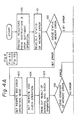
- a microprogram stored in the CPU starts to execute the operation of Fig. 4.
- the contents of all registers of the CPU are protected from destruction, and the software operation controlled by software stored in the MU is stopped.
- the CPU finds the status of the memory error. Namely, the CPU feeds a memory control signal S, for reading out the contents of maintenance register 14 to the memory control circuit 13.
- the circuit 13 reads out the contents of register 14 in response to the signal S, and feeds the read contents as read data signals S 5 to the CPU through the inversion and selection circuit 10.
- the status of the memory error is judged. That is, it is judged whether the memory error is a 1 bit or 2 bit error in accordance with 1 bit error indicating bit 14-1-1 and 2 bit error indicating bit 14-1-2 of the maintenance register 14.
- the operation of point 103 is carried out.
- the CPU sets a write back (rewrite) and check operation mode. This is carried out by feeding a control signal S 1 to the memory control circuit 13 and by feeding certain instruction data with address data S 3 so as to set a rewrite and check operation mode indicating bit 14-5 of the maintenance register 14 to "1".
- the CPU feeds an instruction for starting a rewrite and check operation. That is, the CPU instructs the MU to read out again the contents of the memory address x where the memory error was detected.
- the MU executes the rewrite and check operation in response to this instruction.
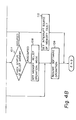
- the CPU finds the result of the rewrite and check operation executed by the MU.
- the MU performs the rewrite and check operation and thereafter feeds a memory response signal S 2 to the CPU.
- the CPU feeds a memory control signal S 1 for reading out the contents of the maintenance register 14 to the memory control circuit 13.
- the memory control circuit 13 reads out and feeds the contents to the CPU through the inversion and selection circuit 10 as read data signals S s .
- the status of the memory error is judged. That is, it is judged whether there is an error in the read data by checking the content in the 1 bit error indicating bit 14-1-1 of the maintenance register 14. if the content is "1", it is judged that this error cannot be corrected by the operation of the above points 103 to 105.
- the memory error is treated as a hard error due to a permanent fault of a memory cell. Then, the operation at point 107 for relieving the faulty bit using relief memory 4 is carried out.
- the CPU checks whether the memory block of the relief memory 4 corresponding to the memory block of the normal memory 3, in which the error address x is included, is occupied or unoccupied (used or unused), by checking the relief memory status indicating bits 14-2-1 to 14-2-4 of the maintenance register 14. If any of the memory blocks 4-1 to 4-4 are occupied, their respective relief memory status indicating bits 14-2-1 to 14-2-4 contain "1".
- the operation at a point 108 is carried out.
- the CPU feeds an instruction for setting the memory relief operation mode to the MU.
- This setting is carried out by feeding a control signal S 1 to the memory control circuit 13 and by feeding certain instruction data with the address data S 3 to the MU.
- the error bit position information Sg which has been stored in the error bit position indicating bit 14-4 of the maintenance register 14 is written into the register (one of the registers 5-1 to 5-4) corresponding to the normal memory block including the error address x.
- the corresponding one of the relief memory condition indicating bits 14-2-1 to 14-2-4 and the corresponding one of the memory relief operation mode indicating bits 14-3-1 to 14-3-4 are set to 111".
- the MU executes a transcription operation from the normal memory 3 to the relief memory 4. This operation is described in detail later.
- the CPU resumes software operation from the error address x (point 109). This software operation is carried out in accordance with the software stored in the MU.
- the program proceeds to a point 110 wherein an interrupt source of the memory fault is set, whereupon the operation is completed (terminated). Furthermore, if it is judged at the point 102 that the memory error is a 2 bit error, since the error correction cannot save it, the program also proceeds to the above point 110 and an interrupt source of the memory fault is set.
- Figure 5 indicates the rewrite and check operation executed by the MU.
- the MU starts this rewrite and check operation of Fig. 5.
- the contents in the error address x of the normal memory 3 are read out again in accordance with the memory address signal S 3 which is fed from the CPU with the memory control signal S, instructing to read out data from the normal memory 3.
- the read data is temporarily set (stored) in the read data register 6 and then applied to the inversion and selection circuit 10 and to the error detecting circuit 9 through the selection circuit 8.
- the read data is checked for error by the error detecting circuit 9.
- the status of the memory error is judged in response to the error detection signal S a . If a 1 bit error is detected, the program proceeds to a point 203 wherein the error bit is corrected. That is, in response to the error bit position information Sg from the error detecting circuit 9, the inversion and selection circuit 10 inverts the error bit in the read data which is fed thereto through the selection circuit 8.
- the corrected read data is, at a point 204, fed from circuit 10 to the normal memory 3 through the distribution and selection circuit 2 and then rewritten in the address x of the normal memory 3.
- the status of the memory error is judged in response to the error detecting signal S a from the error detecting circuit 9. If the memory error detected at the point 202 is a temporary error, since the error is corrected by the inversion and selection circuit 10 using ECC, no error will be detected at the point 207. Namely the temporary error has been corrected by the rewrite operation. In that case, the program proceeds to a point 210 wherein the memory control circuit 13 feeds a memory response signal S 2 to the CPU. Thus, the MU ends the rewrite and check operation.
- the read data from the normal memory 3 is not sent to the CPU.
- the above memory response signal S 2 is sent after the complete end of the rewrite and check operation. After receiving the memory response signal S 2 , the CPU executes the operation at point 105 of Fig. 4.
- the program proceeds to a point 209 wherein the status of the memory error is set to the maintenance register 14.
- the 1 bit error indicating bit 14-1-1 of the maintenance register 14 is set to "1" by means of the error detection signal S a from the error detecting circuit 9.
- the program proceeds to the point 209 wherein the 2 bit error indicating bit 14-1-2 of the maintenance register 14 is set to "1" by the error detection signal S a from the error detecting circuit 9.
- the program directly jumps to the point 210 wherein a memory response signal S 2 is fed to the CPU.
- the MU is provided with a relief memory 4 having the four memory blocks 4-1 to 4-4 as mentioned before. If a hard error occurs in one of the sub-blocks 3-1-1 to 3-4-39 in the normal memory 3, the one of the memory blocks 4-1 to 4-4 which corresponds to the normal memory block including the faulty sub-block is used to relieve the faulty sub-block.
- the MU is further provided with registers 5-1 to 5-4 for storing the bit position (sub-block position) of a hard error, which registers 5-1 to 5-4 correspond to the memory blocks 3-1 to 3-4, respectively.
- the relief memory condition indicating bits 14-2-1 to 14-2-4 and the memory relief operation mode indicating bits 14-3-1 to 14-3-4 are provided as mentioned before.
- the contents at a memory relief address y in the memory block 3-2, forming one word of data, are read out to the read data register 6 and then fed to the error detecting circuit 9 and to the inversion and selctive circuit 10 through the selection circuit 8.
- the read data word is checked for error by the error detecting circuit 9. Then, at a point 302, the status of the memory error is judged in response to the error detection signal S a from the error detecting circuit 9.
- the program proceeds to a point 303 wherein the error bit is corrected by inverting it at the inversion and selection circuit 10, depending upon the error bit position information Sg from the error detecting circuit 9. Then, the program proceeds to a point 304. If there is no error, the program directly proceeds from the point 302 to the point 304.
- the read data or corrected read data is rewritten into the memory relief address y of both the normal memory block 3-2 and the relief memory block 4-2.
- the sub-block 3-2-1 (I from 1 to 39) includes a faulty cell; the read data or corrected read data of the bit position of / is rewritten into the memory relief address y of both the sub-block 3-2-1 and the relief memory block 4-2.
- Other read data of bit positions different from / that is, the rest of the word is rewritten into the memory relief address y of the respective sub-blocks of the normal memory block 3-2.
- the above distribution of the rewrite data is executed by the distribution and selection circuit 2 in accordance with the value / in the register 5-2.
- a similar transcription operation is carried out in sequence from the first word (first memory address) to the 256 K-th word at (memory address 256 K) of the memory block 3-2 in response to the refresh timing signal S f .
- the transcription operation mode ends.
- the relief memory block 4-2 relieves the sub-block 3-2-i including the faulty cell, all the data of all memory addresses (1 to 256 K) in the sub-block 3-2-1 is transcribed into the relief memory block 4-2 after correcting the error data from the faulty cell.
- the above-mentioned one-word transcription operation of Fig. 6 is executed every time the refresh timing signal S f is produced.
- the memory refresh period which is a dead period of time for accessing the MU from the CPU, is used for executing the transcription operation.
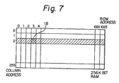
- FIG. 7 indicates a memory cell array of a dynamic RAM of 256 K bit. In this RAM, all cells (1024 bits) in a column are simultaneously refreshed at an interval of 15 usec. All cells in the RAM (256 columns) can be refreshed in about 4 msec. As is known, in Fig. 7, if a refresh address (column address) of "2" and a row address of "3" are applied to the RAM, the contents in a cell 18 are read out.
- Figure 8 illustrates a circuit for forming the memory relief address y and a start signal of the transcription operation.
- the memory relief address y is composed of the refresh address (column address) S d , produced by the refresh address counter 12 having 8 bits and the row address S a , produced by the row address counter 15 having 10 bits.
- a flip-flop 19 for indicating the memory relief operation mode is set by the instruction for setting the memory relief operation mode fed from the CPU. During this mode, therefore, the flip-flop 19 outputs a signal of "1".
- a flip-flop 20 is used for indicating the relief memory condition, namely whether it is occupied or unoccupied. When unoccupied, a signal of "0" is output from the flip-flop 20.
- the refresh timing signal S f which is produced at an interval of 15 psec, is applied to the refresh address counter 12 for counting.
- the refresh address counter 12 has counted up to "255", that is, when the column address becomes "255”, an overflow signal So is produced.
- the first refresh start signal S is input following the first overflow signal S c to be produced, a flip-flop 21 is set causing a signal (memory relief operation signal) of "1" to output.
- This output signal of "1" from the flip-flop 21 in fact indicates that it is under the memory relief operation. Therefore, during this memory relief operation, when the refresh timing signal S f is produced, the start signal for starting the transcription operation (operation of Fig. 6) is produced.
- the row address counter 15 is counted up (incremented).
- the memory relief operation signal is also used for switching the distribution and selection circuit 2 so as to select the data from the inversion and selection circuit 10 instead of the write data from the write data register 1.
- the transcript;on operation is completed for all the words of 256 K in the memory block 3-2 (where each sub-memory and relief memory block is composed of a dynamic RAM of 256 K bits).
- the flip-flop 19 and 20 are reset and the flip-flop 20 is set.
- the memory relief operation indicating bit 14-3-2 of the maintenance register 14 (Fig. 2) is cleared.
- the information / indicating the bit position (sub-block position) of the faulty cell has been stored in the register 5-2.
- the MU is not allowed to be accessed by the CPU and the DCH, etc.
- the memory refresh period is a dead period of time which cannot be used for a software operation.
- the CPU and the DCH are not employed for so long a time for the memory relief operation.
- the processing capability thereof can be prevented from being greatly decreased.
- a refresh address counter which has been already provided can be used for the relief operation. This enables reduction of the manufacturing cost of the system.
- the relief memory condition indicating bit 14-2-2 corresponding to the memory block 3-2 is set to "1", indicating that relief memory block 4-2 is occupied, and the memory relief operation mode indicating bit 14-3-2 is reset to "0", which means that operation is no longer under the memory relief operation mode.
- the MU resumes the normal operation mode wherein read out data is fed to the CPU or to the DCH before checking for a read data error by the error detection circuit 9 in response to a data read instruction. Therefore, a short access time and high processing speed can be maintained.
- sub-block 3-2-i having the permanent fault is not accessed after the memory relief operation. Instead of the sub-block 3-2-i, the relief memory block 4-2 is accessed. This switching is executed by the distribution and selection circuit 2 in response to the content in the register 5-2.
- the number of memory blocks of the normal and relief memories 3 and 4 can be freely determined.
- the storage capacities of the memory element (RAM) and the memory block are not limited to 256 K bits and 256 K words.
- the word used in the MU is not limited to 39 bits (data of 32 bits and ECC of 7 bits).
- the error detection capability is not limited to 2 bit detection and the error correction capability is not limited to 1 bit correction.
- n bits In order to be able to correct n bits (n>1), it is necessary to provide n registers for storing error bit positions of the hard error for each memory block and to modify the error detection circuit 9, distribution and selection circuit 2, selection circuit 8, and inversion and selection circuit 10, correspondingly.
- Memory relief operations for a plurality of memory blocks may be simultaneously executed. In order to do this, it is necessary to provide a row address counter 15 for each memory block.
- a part of the software operation of the CPU (operation from point 100 to point 103 of Fig. 4) may be partly or wholly executed by the MU.
- the present invention is not limited to an MU and CPU executing a stored program (software) and may also be used for a memory device operated by hardware.
- data processing may be completely stopped during the memory relief operation, which lasts for over 100 msec.
Landscapes
- Engineering & Computer Science (AREA)
- Theoretical Computer Science (AREA)
- Quality & Reliability (AREA)
- Physics & Mathematics (AREA)
- General Engineering & Computer Science (AREA)
- General Physics & Mathematics (AREA)
- Techniques For Improving Reliability Of Storages (AREA)
- For Increasing The Reliability Of Semiconductor Memories (AREA)
Claims (14)
Applications Claiming Priority (2)
| Application Number | Priority Date | Filing Date | Title |
|---|---|---|---|
| JP58039674A JPS59165300A (ja) | 1983-03-10 | 1983-03-10 | メモリ障害訂正方式 |
| JP39674/83 | 1983-03-10 |
Publications (3)
| Publication Number | Publication Date |
|---|---|
| EP0119075A2 EP0119075A2 (de) | 1984-09-19 |
| EP0119075A3 EP0119075A3 (en) | 1988-01-13 |
| EP0119075B1 true EP0119075B1 (de) | 1990-10-24 |
Family
ID=12559640
Family Applications (1)
| Application Number | Title | Priority Date | Filing Date |
|---|---|---|---|
| EP84301592A Expired EP0119075B1 (de) | 1983-03-10 | 1984-03-09 | Verfahren und Gerät zur Bearbeitung eines defekten Speichers |
Country Status (5)
| Country | Link |
|---|---|
| US (1) | US4617660A (de) |
| EP (1) | EP0119075B1 (de) |
| JP (1) | JPS59165300A (de) |
| CA (1) | CA1209269A (de) |
| DE (1) | DE3483434D1 (de) |
Families Citing this family (32)
| Publication number | Priority date | Publication date | Assignee | Title |
|---|---|---|---|---|
| US4692923A (en) * | 1984-09-28 | 1987-09-08 | Ncr Corporation | Fault tolerant memory |
| JPS63176798U (de) * | 1986-12-03 | 1988-11-16 | ||
| DE3866902D1 (de) * | 1987-03-10 | 1992-01-30 | Siemens Ag | Verfahren und einrichtung zur steuerung der fehlerkorrektur innerhalb einer datenuebertragungssteuerung bei von bewegten peripheren speichern, insbesondere plattenspeichern, eines datenverarbeitungssystems gelesenen daten. |
| US6330240B1 (en) | 1987-04-24 | 2001-12-11 | Hitachi, Ltd. | ATM cell switching system |
| JP2865692B2 (ja) * | 1989-02-22 | 1999-03-08 | 株式会社日立製作所 | スイッチングシステム及びその構成方法 |
| US5365519A (en) | 1991-03-05 | 1994-11-15 | Hitachi, Ltd. | ATM switch1ng system connectable to I/O links having different transmission rates |
| USRE36716E (en) * | 1987-07-15 | 2000-05-30 | Hitachi, Ltd. | Switching system for switching cells having error detection apparatus |
| USRE36751E (en) * | 1987-07-15 | 2000-06-27 | Hitachi, Ltd. | ATM switching system connectable to I/O links having different transmission rates |
| JPH0821238B2 (ja) * | 1987-11-12 | 1996-03-04 | 三菱電機株式会社 | 半導体記憶装置 |
| JPH0365726A (ja) * | 1989-08-02 | 1991-03-20 | Shikoku Nippon Denki Software Kk | マイクロプログラム格納方式 |
| JPH0423055A (ja) * | 1990-05-17 | 1992-01-27 | Fujitsu Ltd | 交代割付制御方式 |
| JPH065823A (ja) * | 1992-06-19 | 1994-01-14 | Toshiba Corp | 不揮発性半導体記憶装置及びその使用方法 |
| FR2757305B1 (fr) * | 1996-12-17 | 1999-01-15 | Sgs Thomson Microelectronics | Dispositif et procede de lecture incrementale d'une memoire |
| JP3184129B2 (ja) | 1997-09-29 | 2001-07-09 | 甲府日本電気株式会社 | 記憶装置 |
| JP3177207B2 (ja) | 1998-01-27 | 2001-06-18 | インターナショナル・ビジネス・マシーンズ・コーポレ−ション | リフレッシュ間隔制御装置及び方法、並びにコンピュータ |
| JP4180757B2 (ja) * | 1999-11-05 | 2008-11-12 | 株式会社東芝 | シミュレーション装置 |
| US6701480B1 (en) * | 2000-03-08 | 2004-03-02 | Rockwell Automation Technologies, Inc. | System and method for providing error check and correction in memory systems |
| US7278083B2 (en) * | 2003-06-27 | 2007-10-02 | International Business Machines Corporation | Method and system for optimized instruction fetch to protect against soft and hard errors |
| US7099221B2 (en) * | 2004-05-06 | 2006-08-29 | Micron Technology, Inc. | Memory controller method and system compensating for memory cell data losses |
| US7116602B2 (en) | 2004-07-15 | 2006-10-03 | Micron Technology, Inc. | Method and system for controlling refresh to avoid memory cell data losses |
| KR100643288B1 (ko) * | 2004-11-16 | 2006-11-10 | 삼성전자주식회사 | 플래시 메모리의 데이터 처리 장치 및 방법 |
| KR100643287B1 (ko) * | 2004-11-19 | 2006-11-10 | 삼성전자주식회사 | 플래시 메모리의 데이터 처리 장치 및 방법 |
| US20070094569A1 (en) * | 2005-10-24 | 2007-04-26 | Thayer Larry J | Determining hard errors vs. soft errors in memory |
| JP4736828B2 (ja) * | 2006-02-03 | 2011-07-27 | 株式会社デンソー | 電子制御装置 |
| US7894289B2 (en) | 2006-10-11 | 2011-02-22 | Micron Technology, Inc. | Memory system and method using partial ECC to achieve low power refresh and fast access to data |
| US7900120B2 (en) * | 2006-10-18 | 2011-03-01 | Micron Technology, Inc. | Memory system and method using ECC with flag bit to identify modified data |
| JP6040627B2 (ja) * | 2012-08-15 | 2016-12-07 | 富士通株式会社 | メモリ制御装置、情報処理装置およびメモリ制御装置の制御方法 |
| JP5548789B2 (ja) * | 2013-01-22 | 2014-07-16 | 株式会社日立製作所 | 半導体装置 |
| US9685217B2 (en) * | 2013-07-22 | 2017-06-20 | Taiwan Semiconductor Manufacturing Company Ltd. | Memory device with over-refresh and method thereof |
| CN103942119A (zh) * | 2013-12-26 | 2014-07-23 | 杭州华为数字技术有限公司 | 一种存储器错误的处理方法和装置 |
| US10020822B2 (en) * | 2014-07-21 | 2018-07-10 | Rensselaer Polytechnic Institute | Error tolerant memory system |
| US10268541B2 (en) * | 2016-08-15 | 2019-04-23 | Samsung Electronics Co., Ltd. | DRAM assist error correction mechanism for DDR SDRAM interface |
Family Cites Families (12)
| Publication number | Priority date | Publication date | Assignee | Title |
|---|---|---|---|---|
| JPS54160137A (en) * | 1978-06-09 | 1979-12-18 | Hitachi Ltd | Memory error recovery system |
| US4506362A (en) * | 1978-12-22 | 1985-03-19 | Gould Inc. | Systematic memory error detection and correction apparatus and method |
| US4360915A (en) * | 1979-02-07 | 1982-11-23 | The Warner & Swasey Company | Error detection means |
| US4255808A (en) * | 1979-04-19 | 1981-03-10 | Sperry Corporation | Hard or soft cell failure differentiator |
| JPS598852B2 (ja) * | 1979-07-30 | 1984-02-28 | 富士通株式会社 | エラ−処理方式 |
| JPS6051749B2 (ja) * | 1979-08-31 | 1985-11-15 | 富士通株式会社 | エラ−訂正方式 |
| JPS5942398B2 (ja) * | 1979-12-13 | 1984-10-15 | 富士通株式会社 | エラ−訂正方式 |
| US4380812A (en) * | 1980-04-25 | 1983-04-19 | Data General Corporation | Refresh and error detection and correction technique for a data processing system |
| US4371930A (en) * | 1980-06-03 | 1983-02-01 | Burroughs Corporation | Apparatus for detecting, correcting and logging single bit memory read errors |
| JPS57143799A (en) * | 1981-02-27 | 1982-09-06 | Hitachi Ltd | Storage device |
| JPS57212698A (en) * | 1981-06-23 | 1982-12-27 | Fujitsu Ltd | Data transfer system |
| US4535455A (en) * | 1983-03-11 | 1985-08-13 | At&T Bell Laboratories | Correction and monitoring of transient errors in a memory system |
-
1983
- 1983-03-10 JP JP58039674A patent/JPS59165300A/ja active Pending
-
1984
- 1984-03-05 CA CA000448845A patent/CA1209269A/en not_active Expired
- 1984-03-08 US US06/587,518 patent/US4617660A/en not_active Expired - Fee Related
- 1984-03-09 EP EP84301592A patent/EP0119075B1/de not_active Expired
- 1984-03-09 DE DE8484301592T patent/DE3483434D1/de not_active Expired - Lifetime
Also Published As
| Publication number | Publication date |
|---|---|
| EP0119075A2 (de) | 1984-09-19 |
| CA1209269A (en) | 1986-08-05 |
| DE3483434D1 (de) | 1990-11-29 |
| US4617660A (en) | 1986-10-14 |
| JPS59165300A (ja) | 1984-09-18 |
| EP0119075A3 (en) | 1988-01-13 |
Similar Documents
| Publication | Publication Date | Title |
|---|---|---|
| EP0119075B1 (de) | Verfahren und Gerät zur Bearbeitung eines defekten Speichers | |
| US5495491A (en) | System using a memory controller controlling an error correction means to detect and correct memory errors when and over a time interval indicated by registers in the memory controller | |
| US4393500A (en) | Method of modifying data stored in non-volatile memory and testing for power failure occurring during modification | |
| CA1165451A (en) | Refresh and error detection and correction technique for a data processing system | |
| US4535455A (en) | Correction and monitoring of transient errors in a memory system | |
| EP0986783B1 (de) | Zeitverteilte entfernung von fehlerkorrekturcodes (ecc) zur korrektur von speicherfehlern | |
| US4456993A (en) | Data processing system with error processing apparatus and error processing method | |
| US4483001A (en) | Online realignment of memory faults | |
| US4359771A (en) | Method and apparatus for testing and verifying the operation of error control apparatus within a memory | |
| US4598402A (en) | System for treatment of single bit error in buffer storage unit | |
| GB2153116A (en) | Memory refresh circuit with varying system transparency | |
| US3444526A (en) | Storage system using a storage device having defective storage locations | |
| EP0370529B1 (de) | Mikrorechner mit EEPROM | |
| US7246257B2 (en) | Computer system and memory control method thereof | |
| EP0386719B1 (de) | Steuerungsschaltung zum Zugriff auf partiellen Speicher | |
| US5261084A (en) | Error judgment method | |
| US5479640A (en) | Memory access system including a memory controller with memory redrive circuitry | |
| US5168558A (en) | Apparatus and method for providing distributed control in a main memory unit of a data processing system | |
| JPS6146864B2 (de) | ||
| JPS63187500A (ja) | 半導体記憶装置 | |
| EP0288479B1 (de) | Vorrichtung und verfahren für das vorsehen einer verteilten steuerung in dem hauptspeicher eines datenverarbeitungssystems | |
| JPS59168997A (ja) | コンピユ−タの主記憶パトロ−ル方法 | |
| JPH0423294B2 (de) | ||
| JPS61123957A (ja) | 記憶装置 | |
| JPH01288947A (ja) | バッファメモリ障害処理方式 |
Legal Events
| Date | Code | Title | Description |
|---|---|---|---|
| PUAI | Public reference made under article 153(3) epc to a published international application that has entered the european phase |
Free format text: ORIGINAL CODE: 0009012 |
|
| AK | Designated contracting states |
Designated state(s): DE FR GB SE |
|
| PUAL | Search report despatched |
Free format text: ORIGINAL CODE: 0009013 |
|
| AK | Designated contracting states |
Kind code of ref document: A3 Designated state(s): DE FR GB SE |
|
| 17P | Request for examination filed |
Effective date: 19880321 |
|
| 17Q | First examination report despatched |
Effective date: 19890414 |
|
| GRAA | (expected) grant |
Free format text: ORIGINAL CODE: 0009210 |
|
| AK | Designated contracting states |
Kind code of ref document: B1 Designated state(s): DE FR GB SE |
|
| PGFP | Annual fee paid to national office [announced via postgrant information from national office to epo] |
Ref country code: FR Payment date: 19901030 Year of fee payment: 8 |
|
| ET | Fr: translation filed | ||
| REF | Corresponds to: |
Ref document number: 3483434 Country of ref document: DE Date of ref document: 19901129 |
|
| PGFP | Annual fee paid to national office [announced via postgrant information from national office to epo] |
Ref country code: GB Payment date: 19910226 Year of fee payment: 8 |
|
| PGFP | Annual fee paid to national office [announced via postgrant information from national office to epo] |
Ref country code: SE Payment date: 19910318 Year of fee payment: 8 |
|
| PGFP | Annual fee paid to national office [announced via postgrant information from national office to epo] |
Ref country code: DE Payment date: 19910522 Year of fee payment: 8 |
|
| PLBE | No opposition filed within time limit |
Free format text: ORIGINAL CODE: 0009261 |
|
| STAA | Information on the status of an ep patent application or granted ep patent |
Free format text: STATUS: NO OPPOSITION FILED WITHIN TIME LIMIT |
|
| 26N | No opposition filed | ||
| PG25 | Lapsed in a contracting state [announced via postgrant information from national office to epo] |
Ref country code: GB Effective date: 19920309 |
|
| PG25 | Lapsed in a contracting state [announced via postgrant information from national office to epo] |
Ref country code: SE Effective date: 19920310 |
|
| GBPC | Gb: european patent ceased through non-payment of renewal fee | ||
| PG25 | Lapsed in a contracting state [announced via postgrant information from national office to epo] |
Ref country code: FR Effective date: 19921130 |
|
| PG25 | Lapsed in a contracting state [announced via postgrant information from national office to epo] |
Ref country code: DE Effective date: 19921201 |
|
| REG | Reference to a national code |
Ref country code: FR Ref legal event code: ST |
|
| EUG | Se: european patent has lapsed |
Ref document number: 84301592.6 Effective date: 19921005 |