EP0119352A2 - Ausgangsschaltung eines Speichers - Google Patents
Ausgangsschaltung eines Speichers Download PDFInfo
- Publication number
- EP0119352A2 EP0119352A2 EP83307341A EP83307341A EP0119352A2 EP 0119352 A2 EP0119352 A2 EP 0119352A2 EP 83307341 A EP83307341 A EP 83307341A EP 83307341 A EP83307341 A EP 83307341A EP 0119352 A2 EP0119352 A2 EP 0119352A2
- Authority
- EP
- European Patent Office
- Prior art keywords
- circuit
- output
- pair
- transistors
- bootstrapped
- Prior art date
- Legal status (The legal status is an assumption and is not a legal conclusion. Google has not performed a legal analysis and makes no representation as to the accuracy of the status listed.)
- Withdrawn
Links
- 230000015654 memory Effects 0.000 title claims description 12
- 239000004065 semiconductor Substances 0.000 claims description 6
- 230000003068 static effect Effects 0.000 abstract description 3
- 210000004027 cell Anatomy 0.000 description 2
- 230000007704 transition Effects 0.000 description 2
- 230000003321 amplification Effects 0.000 description 1
- 239000003990 capacitor Substances 0.000 description 1
- 238000010276 construction Methods 0.000 description 1
- 230000000694 effects Effects 0.000 description 1
- 238000005516 engineering process Methods 0.000 description 1
- 238000003199 nucleic acid amplification method Methods 0.000 description 1
- 210000000352 storage cell Anatomy 0.000 description 1
Images

Classifications
-
- H—ELECTRICITY
- H03—ELECTRONIC CIRCUITRY
- H03K—PULSE TECHNIQUE
- H03K19/00—Logic circuits, i.e. having at least two inputs acting on one output; Inverting circuits
- H03K19/01—Modifications for accelerating switching
- H03K19/017—Modifications for accelerating switching in field-effect transistor circuits
- H03K19/01707—Modifications for accelerating switching in field-effect transistor circuits in asynchronous circuits
- H03K19/01714—Modifications for accelerating switching in field-effect transistor circuits in asynchronous circuits by bootstrapping, i.e. by positive feed-back
-
- G—PHYSICS
- G11—INFORMATION STORAGE
- G11C—STATIC STORES
- G11C7/00—Arrangements for writing information into, or reading information out from, a digital store
- G11C7/10—Input/output [I/O] data interface arrangements, e.g. I/O data control circuits, I/O data buffers
- G11C7/1051—Data output circuits, e.g. read-out amplifiers, data output buffers, data output registers, data output level conversion circuits
- G11C7/1057—Data output buffers, e.g. comprising level conversion circuits, circuits for adapting load
-
- G—PHYSICS
- G11—INFORMATION STORAGE
- G11C—STATIC STORES
- G11C7/00—Arrangements for writing information into, or reading information out from, a digital store
- G11C7/10—Input/output [I/O] data interface arrangements, e.g. I/O data control circuits, I/O data buffers
- G11C7/1051—Data output circuits, e.g. read-out amplifiers, data output buffers, data output registers, data output level conversion circuits
- G11C7/106—Data output latches
-
- H—ELECTRICITY
- H03—ELECTRONIC CIRCUITRY
- H03K—PULSE TECHNIQUE
- H03K5/00—Manipulating of pulses not covered by one of the other main groups of this subclass
- H03K5/01—Shaping pulses
- H03K5/02—Shaping pulses by amplifying
- H03K5/023—Shaping pulses by amplifying using field effect transistors
-
- G—PHYSICS
- G11—INFORMATION STORAGE
- G11C—STATIC STORES
- G11C11/00—Digital stores characterised by the use of particular electric or magnetic storage elements; Storage elements therefor
- G11C11/21—Digital stores characterised by the use of particular electric or magnetic storage elements; Storage elements therefor using electric elements
- G11C11/34—Digital stores characterised by the use of particular electric or magnetic storage elements; Storage elements therefor using electric elements using semiconductor devices
- G11C11/40—Digital stores characterised by the use of particular electric or magnetic storage elements; Storage elements therefor using electric elements using semiconductor devices using transistors
- G11C11/401—Digital stores characterised by the use of particular electric or magnetic storage elements; Storage elements therefor using electric elements using semiconductor devices using transistors forming cells needing refreshing or charge regeneration, i.e. dynamic cells
- G11C11/4063—Auxiliary circuits, e.g. for addressing, decoding, driving, writing, sensing or timing
- G11C11/407—Auxiliary circuits, e.g. for addressing, decoding, driving, writing, sensing or timing for memory cells of the field-effect type
- G11C11/409—Read-write [R-W] circuits
- G11C11/4093—Input/output [I/O] data interface arrangements, e.g. data buffers
-
- G—PHYSICS
- G11—INFORMATION STORAGE
- G11C—STATIC STORES
- G11C11/00—Digital stores characterised by the use of particular electric or magnetic storage elements; Storage elements therefor
- G11C11/21—Digital stores characterised by the use of particular electric or magnetic storage elements; Storage elements therefor using electric elements
- G11C11/34—Digital stores characterised by the use of particular electric or magnetic storage elements; Storage elements therefor using electric elements using semiconductor devices
- G11C11/40—Digital stores characterised by the use of particular electric or magnetic storage elements; Storage elements therefor using electric elements using semiconductor devices using transistors
- G11C11/41—Digital stores characterised by the use of particular electric or magnetic storage elements; Storage elements therefor using electric elements using semiconductor devices using transistors forming static cells with positive feedback, i.e. cells not needing refreshing or charge regeneration, e.g. bistable multivibrator or Schmitt trigger
- G11C11/413—Auxiliary circuits, e.g. for addressing, decoding, driving, writing, sensing, timing or power reduction
- G11C11/417—Auxiliary circuits, e.g. for addressing, decoding, driving, writing, sensing, timing or power reduction for memory cells of the field-effect type
- G11C11/419—Read-write [R-W] circuits
Definitions
- This invention relates to semiconductor memories and in particular to output circuits for such memories.
- Semiconductor memories e.g. static random access memories, comprise an array of storage cells in which data is stored in the form of binary ones and zeros. Since the quantity of energy stored in an individual cell is extremely small it is essential to provide some means of amplification to effect read-out from the memory.
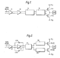
- the standard output chain in a static memory consists of a number of cascaded amplifiers to boost the energy read from a cell. Only the final one or two stages are driven into a limiting condition in order to provide clearly defined logic levels at the output.
- the output chain comprises two or more preamplifiers 12 and 13 which feed a pair of output transistors TRI, TR2, via a high gain clipping amplifier 14 and a quad output driver stage 15.
- the output transistors present a high capacitive load, typically 2pF, on the driver stage.
- the driver stage To provide a high operating speed it is necessary for the driver stage to be a high current circuit. This in turn presents a large load to the clipping amplifiers.
- the overall design thus consumes excessive power and has a poor delay-power product.
- the object of the present invention is to minimise or to overcome this disadvantage.
- a semiconductor memory output circuit including an output transistor series pair, characterised in that each transistor of the pair is coupled to a bootstrapped respective driver circuit, and that means are provided for driving said bootstrapped driver circuits with signals corresponding to memory output data.
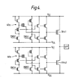
- the memory output chain which is fabricated typically in NMOS technology, comprises a preamplifier 21 provided with positive capacitive feedback via capacitors C211, C212 and coupled to the memory data buses via a first preamplifier or sense amplifier 22.
- the output of the preamplifier 21 is coupled via a logic level converter/gating circuit 23 to a pair of bootstrapped output driver circuits 241, 242.
- Each driver circuit drives a respective one of a series pair of output transistors TR251, TR252.
- Bootstrapped driver circuits are used in this application as they are capable of driving the high capacitive loads presented by the gates of the output transistors whilst consuming very low continuous supply current. Furthermore, these bootstrapped driver circuits present very little capacitive loading to the previous stage and may be controlled by a small input signal. Thus the constraints on preceding stages are significantly reduced.
- Fig. 2 The circuitry of Fig. 2 is shown in some detail in Figs. 3, 4. It should be noted that the associated power-down and gating circuitry, and some additional bootstrap assistance circuitry, has been omitted for clarity.
- the first input preamplifier (22) is fed by signals from a data bus pair DB, DB.
- Differential voltages are amplified by the "long tail pair” configuration and applied to the inputs of the second preamplifier (21).
- This preamplifier is also arranged as a "long tail pair' but controlled positive feedback is used to improve signal rise and fall times.
- the differential output signal from the second preamplifier is of the order of 2 volts.
- the purpose of the next stage is to convert these 2 volt differential voltages to a logic signal suitable for driving the bootstrapped circuits.
- a suitable signal would have a logical zero level of less than 0.5 volts and have fast transitions between logic states.
- the driven cross-coupled arrangement shown in Fig. 3 fulfills these requirements and provides a logical one output level of the order of 3 volts with a 5 volt supply.
- the amount of hysteresis and the speed of transitions may be controlled by the ratio of dimensions between the enhancement and the natural transistors in the cross-couple.
- the outputs DRIV, DRIV go to the inputs of the bootstrap driver circuits shown in Fig. 4.
- the logic level convertor of Fig. 3 comprises a pair of source follower transistors TR31, TR32 each provided with a source load comprising a further transistor 311, 321 or advantageously, two or more parallel converted transistors. These load transistors are cross-coupled and their sources are connected to the circuit ground.
- each driver circuit 40a, 40b there are two bootstrapped driver circuits 40a, 40b, one for each output transistor TR41, TR42. Dimensions in each driver circuit may be optimised individually to match the different loads presented by each output transistor.
- a bootstrapped driver circuit is described in detail in our published specification No. 1,520,078 (Obermeier 4).
- the circuit used in Fig. 4 differs from that of specification No. 1,520.078 in the use of depletion transistor loads and the provision of an extra inverter to permit fast operation from the 0/3 volt logic levels provided by the DRIV, DRIV input signals.
Landscapes
- Physics & Mathematics (AREA)
- Engineering & Computer Science (AREA)
- Computer Hardware Design (AREA)
- Computing Systems (AREA)
- General Engineering & Computer Science (AREA)
- Mathematical Physics (AREA)
- Nonlinear Science (AREA)
- Dram (AREA)
- Logic Circuits (AREA)
- Static Random-Access Memory (AREA)
Applications Claiming Priority (2)
| Application Number | Priority Date | Filing Date | Title |
|---|---|---|---|
| GB08301057A GB2133946B (en) | 1983-01-14 | 1983-01-14 | Memory output circuit |
| GB8301057 | 1983-01-14 |
Publications (2)
| Publication Number | Publication Date |
|---|---|
| EP0119352A2 true EP0119352A2 (de) | 1984-09-26 |
| EP0119352A3 EP0119352A3 (de) | 1987-05-20 |
Family
ID=10536365
Family Applications (1)
| Application Number | Title | Priority Date | Filing Date |
|---|---|---|---|
| EP83307341A Withdrawn EP0119352A3 (de) | 1983-01-14 | 1983-12-02 | Ausgangsschaltung eines Speichers |
Country Status (4)
| Country | Link |
|---|---|
| US (1) | US4583203A (de) |
| EP (1) | EP0119352A3 (de) |
| JP (1) | JPS59140689A (de) |
| GB (1) | GB2133946B (de) |
Cited By (3)
| Publication number | Priority date | Publication date | Assignee | Title |
|---|---|---|---|---|
| DE3524662A1 (de) * | 1985-07-10 | 1987-01-22 | Siemens Ag | Verfahren und schaltungsanordnung zur verkuerzung der lesezugriffszeit bei einem ecl-speicher |
| DE3700403A1 (de) * | 1986-01-17 | 1987-07-23 | Mitsubishi Electric Corp | Halbleiterspeichereinrichtung |
| EP0259861A1 (de) * | 1986-09-09 | 1988-03-16 | Nec Corporation | Mit verringertem Energieverbrauch arbeitende Pufferschaltung |
Families Citing this family (24)
| Publication number | Priority date | Publication date | Assignee | Title |
|---|---|---|---|---|
| KR890003373B1 (ko) * | 1986-11-30 | 1989-09-19 | 삼성전자 주식회사 | 씨모오스 반도체 메모리 장치의 입출력 회로 |
| DE3739467A1 (de) * | 1987-11-21 | 1989-06-01 | Philips Nv | Schaltungsanordnung fuer eine doppel-busleitung |
| JPH01226213A (ja) * | 1988-03-04 | 1989-09-08 | Mitsubishi Electric Corp | ドライバ回路 |
| US4964083A (en) * | 1989-04-27 | 1990-10-16 | Motorola, Inc. | Non-address transition detection memory with improved access time |
| KR920000962B1 (ko) * | 1989-05-26 | 1992-01-31 | 삼성전자 주식회사 | 반도체 메모리 장치의 데이터 출력단 전압레벨 조절회로 |
| JP3059737B2 (ja) * | 1989-12-25 | 2000-07-04 | シャープ株式会社 | 半導体記憶装置 |
| US5089789A (en) * | 1990-05-16 | 1992-02-18 | Texas Instruments Incorporated | Differential amplifier |
| JP3094469B2 (ja) * | 1991-01-18 | 2000-10-03 | ソニー株式会社 | 出力バッファ回路 |
| US5257238A (en) * | 1991-07-11 | 1993-10-26 | Micron Technology, Inc. | Dynamic memory having access transistor turn-off state |
| DE4128290C1 (de) * | 1991-08-27 | 1992-12-03 | Samsung Electronics Co., Ltd., Suwon, Kr | |
| US5387826A (en) * | 1993-02-10 | 1995-02-07 | National Semiconductor Corporation | Overvoltage protection against charge leakage in an output driver |
| JP3071605B2 (ja) * | 1993-04-23 | 2000-07-31 | 日本電気株式会社 | 半導体記憶装置 |
| US5406140A (en) * | 1993-06-07 | 1995-04-11 | National Semiconductor Corporation | Voltage translation and overvoltage protection |
| WO1994029961A1 (en) * | 1993-06-07 | 1994-12-22 | National Semiconductor Corporation | Overvoltage protection |
| US5793225A (en) * | 1996-01-02 | 1998-08-11 | Pmc-Sierra, Inc. | CMOS SONET/ATM receiver suitable for use with pseudo ECL and TTL signaling environments |
| EP0821362B1 (de) | 1996-07-24 | 2004-05-26 | STMicroelectronics S.r.l. | Ausgabestufe für Speicheranlage und für Niederspannungsanwendungen |
| TW361010B (en) * | 1996-09-30 | 1999-06-11 | Hitachi Ltd | Semiconductor device |
| JPH10188574A (ja) * | 1996-12-20 | 1998-07-21 | Nec Corp | 半導体記憶装置 |
| US5945847A (en) * | 1997-05-20 | 1999-08-31 | Lucent Technologies | Distributed amplifier logic designs |
| US5900750A (en) * | 1997-08-15 | 1999-05-04 | Lsi Logic Corporation | 5V output driver on 2.5V technology |
| GB2349996A (en) | 1999-05-12 | 2000-11-15 | Sharp Kk | Voltage level converter for an active matrix LCD |
| US6300800B1 (en) | 1999-11-24 | 2001-10-09 | Lsi Logic Corporation | Integrated circuit I/O buffer with series P-channel and floating well |
| US7148723B2 (en) | 2002-01-30 | 2006-12-12 | Caterpillar Inc | Common controller area network interface |
| KR100857875B1 (ko) | 2007-03-05 | 2008-09-10 | 주식회사 하이닉스반도체 | 반도체 소자의 라이트 드라이버 |
Family Cites Families (1)
| Publication number | Priority date | Publication date | Assignee | Title |
|---|---|---|---|---|
| DE2521949A1 (de) * | 1975-05-16 | 1976-11-25 | Itt Ind Gmbh Deutsche | Monolithisch integrierbare mis- treiberstufe |
-
1983
- 1983-01-14 GB GB08301057A patent/GB2133946B/en not_active Expired
- 1983-12-02 EP EP83307341A patent/EP0119352A3/de not_active Withdrawn
- 1983-12-08 US US06/559,251 patent/US4583203A/en not_active Expired - Fee Related
- 1983-12-27 JP JP58252231A patent/JPS59140689A/ja active Pending
Non-Patent Citations (2)
| Title |
|---|
| IBM TECHNICAL DISCLOSURE BULLETIN, vol. 16, no. 4, September 1973, pages 1272-1273, New York, US; D.T. COX et al.: "Bootstrap capacitor control" * |
| IEEE JOURNAL OF SOLID-STATE CIRCUITS, vol. SC-15, no. 3, June 1980, pages 346-353, IEEE, New York, US; T. HAGIWARA et al.: "A 16 kbit electrically erasable PROM using n-channel Si-gate MNOS technology" * |
Cited By (3)
| Publication number | Priority date | Publication date | Assignee | Title |
|---|---|---|---|---|
| DE3524662A1 (de) * | 1985-07-10 | 1987-01-22 | Siemens Ag | Verfahren und schaltungsanordnung zur verkuerzung der lesezugriffszeit bei einem ecl-speicher |
| DE3700403A1 (de) * | 1986-01-17 | 1987-07-23 | Mitsubishi Electric Corp | Halbleiterspeichereinrichtung |
| EP0259861A1 (de) * | 1986-09-09 | 1988-03-16 | Nec Corporation | Mit verringertem Energieverbrauch arbeitende Pufferschaltung |
Also Published As
| Publication number | Publication date |
|---|---|
| GB8301057D0 (en) | 1983-02-16 |
| JPS59140689A (ja) | 1984-08-13 |
| EP0119352A3 (de) | 1987-05-20 |
| GB2133946B (en) | 1986-02-26 |
| GB2133946A (en) | 1984-08-01 |
| US4583203A (en) | 1986-04-15 |
Similar Documents
| Publication | Publication Date | Title |
|---|---|---|
| US4583203A (en) | Memory output circuit | |
| US4931994A (en) | Static semiconductor memory with section and block sense amplifiers | |
| US4618785A (en) | CMOS sense amplifier with level shifter | |
| EP0098060A2 (de) | Taktimpulsgeneratorschaltung | |
| US4695748A (en) | Comparing device | |
| KR100303735B1 (ko) | 메모리회로 | |
| US4649301A (en) | Multiple-input sense amplifier with two CMOS differential stages driving a high-gain stage | |
| US4871933A (en) | High-speed static differential sense amplifier | |
| US4871978A (en) | High-speed static differential sense amplifier | |
| KR870002592A (ko) | 메모리 회로 | |
| KR960001860B1 (ko) | 반도체집적회로의 데이타 입출력선 센싱회로 | |
| EP0750310A1 (de) | Hochgeschwindigkeitsdifferentialstromleseverstärker mit positiver Rückmeldung | |
| US4860257A (en) | Level shifter for an input/output bus in a CMOS dynamic ram | |
| EP0499460A2 (de) | Halbleiterspeicheranordnung | |
| JPS6374196A (ja) | Cmos半導体メモリ回路 | |
| US5083295A (en) | Integrated memory circuit with interconnected sense amplifiers | |
| US4658160A (en) | Common gate MOS differential sense amplifier | |
| US5724299A (en) | Multiport register file memory using small voltage swing for write operation | |
| KR100692988B1 (ko) | 반도체 기억 장치 | |
| US4825409A (en) | NMOS data storage cell for clocked shift register applications | |
| EP0060115A2 (de) | Statische RAM-Speicherschaltung | |
| US4627031A (en) | CMOS memory arrangement | |
| US4707808A (en) | Small size, high speed GaAs data latch | |
| US4636988A (en) | CMOS memory arrangement with reduced data line compacitance | |
| CN1144226C (zh) | 读出放大器电路 |
Legal Events
| Date | Code | Title | Description |
|---|---|---|---|
| PUAI | Public reference made under article 153(3) epc to a published international application that has entered the european phase |
Free format text: ORIGINAL CODE: 0009012 |
|
| AK | Designated contracting states |
Designated state(s): DE FR IT NL |
|
| PUAL | Search report despatched |
Free format text: ORIGINAL CODE: 0009013 |
|
| AK | Designated contracting states |
Kind code of ref document: A3 Designated state(s): DE FR IT NL |
|
| STAA | Information on the status of an ep patent application or granted ep patent |
Free format text: STATUS: THE APPLICATION IS DEEMED TO BE WITHDRAWN |
|
| 18D | Application deemed to be withdrawn |
Effective date: 19871121 |
|
| RIN1 | Information on inventor provided before grant (corrected) |
Inventor name: MONK, TREVOR KENNETH |