EP0119400B1 - MOSFET de type vertical et procédé pour sa fabrication - Google Patents
MOSFET de type vertical et procédé pour sa fabrication Download PDFInfo
- Publication number
- EP0119400B1 EP0119400B1 EP84100612A EP84100612A EP0119400B1 EP 0119400 B1 EP0119400 B1 EP 0119400B1 EP 84100612 A EP84100612 A EP 84100612A EP 84100612 A EP84100612 A EP 84100612A EP 0119400 B1 EP0119400 B1 EP 0119400B1
- Authority
- EP
- European Patent Office
- Prior art keywords
- wafer
- portions
- regions
- forming
- well regions
- Prior art date
- Legal status (The legal status is an assumption and is not a legal conclusion. Google has not performed a legal analysis and makes no representation as to the accuracy of the status listed.)
- Expired
Links
- 238000004519 manufacturing process Methods 0.000 title claims description 9
- 238000000034 method Methods 0.000 claims description 72
- VYPSYNLAJGMNEJ-UHFFFAOYSA-N Silicium dioxide Chemical compound O=[Si]=O VYPSYNLAJGMNEJ-UHFFFAOYSA-N 0.000 claims description 24
- 229910052814 silicon oxide Inorganic materials 0.000 claims description 24
- 238000005468 ion implantation Methods 0.000 claims description 20
- 229910021420 polycrystalline silicon Inorganic materials 0.000 claims description 20
- 229920005591 polysilicon Polymers 0.000 claims description 20
- 238000009792 diffusion process Methods 0.000 claims description 18
- 239000012535 impurity Substances 0.000 claims description 16
- 230000003647 oxidation Effects 0.000 claims description 15
- 238000007254 oxidation reaction Methods 0.000 claims description 15
- 239000004065 semiconductor Substances 0.000 claims description 11
- 238000010438 heat treatment Methods 0.000 claims description 9
- XUIMIQQOPSSXEZ-UHFFFAOYSA-N Silicon Chemical compound [Si] XUIMIQQOPSSXEZ-UHFFFAOYSA-N 0.000 claims description 6
- 229910052710 silicon Inorganic materials 0.000 claims description 6
- 239000010703 silicon Substances 0.000 claims description 6
- 238000000151 deposition Methods 0.000 claims description 2
- 230000001590 oxidative effect Effects 0.000 claims description 2
- 239000012212 insulator Substances 0.000 claims 4
- -1 boron ion Chemical class 0.000 description 20
- 229910052581 Si3N4 Inorganic materials 0.000 description 11
- 229910052698 phosphorus Inorganic materials 0.000 description 11
- 239000011574 phosphorus Substances 0.000 description 11
- HQVNEWCFYHHQES-UHFFFAOYSA-N silicon nitride Chemical compound N12[Si]34N5[Si]62N3[Si]51N64 HQVNEWCFYHHQES-UHFFFAOYSA-N 0.000 description 11
- 239000000758 substrate Substances 0.000 description 11
- 229910052796 boron Inorganic materials 0.000 description 9
- 238000005229 chemical vapour deposition Methods 0.000 description 9
- XAGFODPZIPBFFR-UHFFFAOYSA-N aluminium Chemical compound [Al] XAGFODPZIPBFFR-UHFFFAOYSA-N 0.000 description 8
- 229910052782 aluminium Inorganic materials 0.000 description 8
- 239000011248 coating agent Substances 0.000 description 8
- 238000000576 coating method Methods 0.000 description 8
- 238000001771 vacuum deposition Methods 0.000 description 7
- 229910021421 monocrystalline silicon Inorganic materials 0.000 description 6
- IJGRMHOSHXDMSA-UHFFFAOYSA-N Atomic nitrogen Chemical compound N#N IJGRMHOSHXDMSA-UHFFFAOYSA-N 0.000 description 5
- 229910052785 arsenic Inorganic materials 0.000 description 5
- 238000001259 photo etching Methods 0.000 description 5
- 230000000694 effects Effects 0.000 description 4
- 230000002093 peripheral effect Effects 0.000 description 4
- RQNWIZPPADIBDY-UHFFFAOYSA-N arsenic atom Chemical compound [As] RQNWIZPPADIBDY-UHFFFAOYSA-N 0.000 description 3
- 238000005530 etching Methods 0.000 description 3
- 239000011521 glass Substances 0.000 description 3
- 238000002513 implantation Methods 0.000 description 3
- NBIIXXVUZAFLBC-UHFFFAOYSA-N Phosphoric acid Chemical compound OP(O)(O)=O NBIIXXVUZAFLBC-UHFFFAOYSA-N 0.000 description 2
- OAICVXFJPJFONN-UHFFFAOYSA-N Phosphorus Chemical compound [P] OAICVXFJPJFONN-UHFFFAOYSA-N 0.000 description 2
- 238000005275 alloying Methods 0.000 description 2
- 229910052757 nitrogen Inorganic materials 0.000 description 2
- 230000002411 adverse Effects 0.000 description 1
- 229910045601 alloy Inorganic materials 0.000 description 1
- 239000000956 alloy Substances 0.000 description 1
- 229910000147 aluminium phosphate Inorganic materials 0.000 description 1
- 238000011161 development Methods 0.000 description 1
- 230000018109 developmental process Effects 0.000 description 1
- 238000001312 dry etching Methods 0.000 description 1
Images




Classifications
-
- H—ELECTRICITY
- H10—SEMICONDUCTOR DEVICES; ELECTRIC SOLID-STATE DEVICES NOT OTHERWISE PROVIDED FOR
- H10D—INORGANIC ELECTRIC SEMICONDUCTOR DEVICES
- H10D30/00—Field-effect transistors [FET]
- H10D30/60—Insulated-gate field-effect transistors [IGFET]
- H10D30/64—Double-diffused metal-oxide semiconductor [DMOS] FETs
- H10D30/66—Vertical DMOS [VDMOS] FETs
-
- H—ELECTRICITY
- H10—SEMICONDUCTOR DEVICES; ELECTRIC SOLID-STATE DEVICES NOT OTHERWISE PROVIDED FOR
- H10D—INORGANIC ELECTRIC SEMICONDUCTOR DEVICES
- H10D30/00—Field-effect transistors [FET]
- H10D30/01—Manufacture or treatment
- H10D30/021—Manufacture or treatment of FETs having insulated gates [IGFET]
- H10D30/028—Manufacture or treatment of FETs having insulated gates [IGFET] of double-diffused metal oxide semiconductor [DMOS] FETs
- H10D30/0291—Manufacture or treatment of FETs having insulated gates [IGFET] of double-diffused metal oxide semiconductor [DMOS] FETs of vertical DMOS [VDMOS] FETs
-
- H—ELECTRICITY
- H10—SEMICONDUCTOR DEVICES; ELECTRIC SOLID-STATE DEVICES NOT OTHERWISE PROVIDED FOR
- H10D—INORGANIC ELECTRIC SEMICONDUCTOR DEVICES
- H10D30/00—Field-effect transistors [FET]
- H10D30/60—Insulated-gate field-effect transistors [IGFET]
- H10D30/64—Double-diffused metal-oxide semiconductor [DMOS] FETs
- H10D30/66—Vertical DMOS [VDMOS] FETs
- H10D30/662—Vertical DMOS [VDMOS] FETs having a drift region having a doping concentration that is higher between adjacent body regions relative to other parts of the drift region
-
- H—ELECTRICITY
- H10—SEMICONDUCTOR DEVICES; ELECTRIC SOLID-STATE DEVICES NOT OTHERWISE PROVIDED FOR
- H10D—INORGANIC ELECTRIC SEMICONDUCTOR DEVICES
- H10D64/00—Electrodes of devices having potential barriers
- H10D64/20—Electrodes characterised by their shapes, relative sizes or dispositions
- H10D64/27—Electrodes not carrying the current to be rectified, amplified, oscillated or switched, e.g. gates
- H10D64/311—Gate electrodes for field-effect devices
- H10D64/411—Gate electrodes for field-effect devices for FETs
- H10D64/511—Gate electrodes for field-effect devices for FETs for IGFETs
- H10D64/514—Gate electrodes for field-effect devices for FETs for IGFETs characterised by the insulating layers
- H10D64/516—Gate electrodes for field-effect devices for FETs for IGFETs characterised by the insulating layers the thicknesses being non-uniform
-
- H—ELECTRICITY
- H10—SEMICONDUCTOR DEVICES; ELECTRIC SOLID-STATE DEVICES NOT OTHERWISE PROVIDED FOR
- H10D—INORGANIC ELECTRIC SEMICONDUCTOR DEVICES
- H10D62/00—Semiconductor bodies, or regions thereof, of devices having potential barriers
- H10D62/10—Shapes, relative sizes or dispositions of the regions of the semiconductor bodies; Shapes of the semiconductor bodies
- H10D62/13—Semiconductor regions connected to electrodes carrying current to be rectified, amplified or switched, e.g. source or drain regions
- H10D62/149—Source or drain regions of field-effect devices
- H10D62/151—Source or drain regions of field-effect devices of IGFETs
-
- H—ELECTRICITY
- H10—SEMICONDUCTOR DEVICES; ELECTRIC SOLID-STATE DEVICES NOT OTHERWISE PROVIDED FOR
- H10D—INORGANIC ELECTRIC SEMICONDUCTOR DEVICES
- H10D62/00—Semiconductor bodies, or regions thereof, of devices having potential barriers
- H10D62/10—Shapes, relative sizes or dispositions of the regions of the semiconductor bodies; Shapes of the semiconductor bodies
- H10D62/13—Semiconductor regions connected to electrodes carrying current to be rectified, amplified or switched, e.g. source or drain regions
- H10D62/149—Source or drain regions of field-effect devices
- H10D62/151—Source or drain regions of field-effect devices of IGFETs
- H10D62/156—Drain regions of DMOS transistors
- H10D62/157—Impurity concentrations or distributions
-
- H—ELECTRICITY
- H10—SEMICONDUCTOR DEVICES; ELECTRIC SOLID-STATE DEVICES NOT OTHERWISE PROVIDED FOR
- H10D—INORGANIC ELECTRIC SEMICONDUCTOR DEVICES
- H10D64/00—Electrodes of devices having potential barriers
- H10D64/20—Electrodes characterised by their shapes, relative sizes or dispositions
- H10D64/27—Electrodes not carrying the current to be rectified, amplified, oscillated or switched, e.g. gates
- H10D64/311—Gate electrodes for field-effect devices
- H10D64/411—Gate electrodes for field-effect devices for FETs
- H10D64/511—Gate electrodes for field-effect devices for FETs for IGFETs
- H10D64/517—Gate electrodes for field-effect devices for FETs for IGFETs characterised by the conducting layers
- H10D64/518—Gate electrodes for field-effect devices for FETs for IGFETs characterised by the conducting layers characterised by their lengths or sectional shapes
Definitions
- the present invention relates to a vertical-type MOSFET comprising a semiconductor waferfunc- tioning as drain region, a drain electrode joined to the lower surface of said wafer, a plurality of well regions formed in the upper surface of said wafer spaced from each other, a plurality of source regions each of which is formed in one of said well regions respectively, a gate electrode formed on said adjacent well regions and the portion of said wafer between said adjacent well regions and separated from the upper surface of said wafer by a gate insulating film and a source electrode electrically contacting said source regions; and a method for manufacturing said MOSFET.
- a MOSFET is known in accordance with the precharacterising parts of claims 1 and 5 from DE-A-3 114 972.
- 54(3) shows a thyristor structure including a MOSFET in which the gate electrode is more distant from the drain drift region than from the channel region. The gate electrode does not cover the whole portion of the wafer between adjacent well regions.
- EP-A-0 112 607 also falling within the terms of Art. 54(3), a vertical MOSFET is described, the gate electrode of which may be perforated between adjacent well regions in order to reduce the gate to drain capacitance.
- EP-A-0 077 737 again falling under Art. 54(3) discloses a lateral MOSFET with a different configuration providing a shorter distance of the gate electrode from the channel region than from the drain and source regions.
- Fig. 1 a typical cell or chip structure of a prior art vertical-type MOSFET is shown.
- the term "vertical" is derived from the fact that currents flow in the vertical direction of the transistor cell.
- the prior art vertical MOSFET cell is fabricated in accordance with the following fabrication processes;
- both the well region 6 and the source region 7 are formed by the double diffusion method. For this reason, when a large number of transistor elements are fabricated on the silicon wafer, following advantages will accrue. Namely, uniformity in characteristics of each transistor can be obtained. The production yield can be remarkably improved. The transistor device can be small-sized.
- the completed transistor cell has the geometrical configuration in which the polysilicon film exists still in an area corresponding to the upper surface of the drain region, which area corresponds to areas or portions except for the upper surface of the channel region required for the gate electrode. From a structural view point, the gate electrode and the drain region are spaced from each other solely through the thin insulating film interposed therebetween. Accordingly, this results in large capacity between the drain and gate electrodes. Further, the capacity serves as a feedback circuit from the output of the switching element to the input thereof, thereby making it impossible or difficult to effect switching at a high speed.
- the capacity between the drain and gate is reduced without providing adverse effects on the advantages based on the double diffusion method.
- the method is constituted so that the distance between the gate electrode and the drain region is larger than the distance between the gate electrode and well region functioning as channels.
- FIG. 2 there is shown the first embodiment of the invention.
- An example of fabricating processes or steps of an n-channel vertical-type MOSFET according to the first embodiment will be described with reference to Figs. 2(A) to 2(1).
- the method comprises the step of epitaxially growing an N-- type monocrystalline silicon layer 21 of high resistivity, having low donor impurity concentration No of about 2 x 10 15 atoms/cm 3 and thickness of about 15 ⁇ m, on a drain substrate 20 of low resistivity comprising an N +- type monocrystalline silicon wafer of high concentration of donor impurities No of about 1 ⁇ 10 18 atoms/cm 3 to form a drain region 21 of high resistivity.
- a semiconductor wafer 10 is defined by the drain substrate 20 and the drain region 21.
- the method further comprises the steps of covering or coating areas or portions, in which well regions for forming channels will be formed, with a resist 22 on an upper surface of the drain region 21 of high resistivity, effecting dryetching the surface of opened window portions form in the resist 22 by about 1um to form recess portions 21a, and thereafter removing the resist 22.
- the method comprising the steps of depositing a silicon oxide film 23 including therein arsenic (As) having molecular concentration of about 3% by the CVD (Chemical Vapour Deposition) method so that the thickness thereof is 1 ⁇ m on the whole surface thereof, and removing the silicon oxide film 23 except for the recess portions 21a by photo-etching techniques.
- the silicon oxide films 23 filled in the recess portions 21a is formed in such a manner that each upper end is projected from the surface of the drain region 21. More particularly, the silicon oxide films 23 having gradually inclined peripheral edges projected from the surface of the drain region 21.
- the method further comprises the steps of forming a silicon oxide film 24 for a gate on the surface of the drain region by thermal oxidation so that the thickness thereof is approximately 10 2 nm (1,000 A), and forming a polysilicon layer constituting a gate electrode 25 on the upper surface thereof by a CVD method.
- N-type impurities of arsenic (As) contained in the silicon oxide film 23 provided within the recess portions 21a diffuses due to the thermal oxidation mentioned above.
- N +- type regions 23a of high concentration are formed along the interface between the periphery of the silicon oxide film 23 and the drain region 21 of high resistivity.
- the method further comprises the steps of selectively removing by photo-etching techniques the portions of the polysilicon layer in which the well region will be formed, except for gate electrodes 25, effecting boron ion (B + ) implantation with the gate electrode portions 25 serving as a mask, and effecting heat treatment for 24 hours at a temperature of about 1,100°C, whereby a P-type well region 26 for forming channels having depth of 4 to 6 ⁇ m are formed.
- the energy for ion implantation is about 60 KeV, and the implanted quantity thereof is about 4 x 10 13 atoms/cm 2.
- the method further comprises the steps of effecting implantation of boron ion (8 * ) from windows opened in the central portion of the upper surface of the well regions 26 with the resist 27 (shown by dotted line) serving as a mask, and removing the resist 27 upon completion of the ion implantation, whereby regions which will serve as P-type well contact regions are formed in the central portion of the well region 26.
- the energy for ion implantation is about 50 KeV
- the implanted quantity thereof is about 5 x 10 15 atoms/cm 2 .
- the method comprises the steps of covering regions which will serve as P-type well contact regions with resists 28 (shown by dotted lines), and effecting ion implantation of phosphorus ion (P + ) with the resists 28 and the gate electrodes 25 serving as a mask.
- the energy for ion implantation is about 100 KeV, and the implanted quantity is 5 x 10 15 atoms/cm 2 .
- the phosphorus ion is also entered into the polysilicon layer 25.
- resists 28 are removed.
- the regions which will serve as a source region including a phosphorus ion (P+) are formed along the periphery of the regions which will serve as the well contact region.
- the method comprises the steps of forming an insulating film 29 essentially consisting of phosphoric glass in which molecular concentration of phosphorus (P) is about 3% and the thickness thereof is 7 x 10 2 nm (7,000 A) so as to cover the whole surface, and effecting heat treatment in an atmosphere of nitrogen (N 2 ) at a temperature of about 1,050 C, whereby boron ion (B + ) and phosphorus ion (P + ) diffuse from the center to the periphery within the well region 26 to complete a P-type well contact region 30 and N +- type source regions 31 respectively.
- P molecular concentration of phosphorus
- N 2 nitrogen
- the method further comprises the steps of opening windows for the surface of the source region 31 and the well contact region 30 as well as windows for the leading-out port (not shown) of the gate electrodes, thereafter coating aluminum (Al) on the surface thereof by vacuum deposition so that the thickness thereof is 1.5 pm, forming a source electrode 32 and a lead electrode for a gate (not shown) by etching, coating aluminum (AI) having the thickness of about 1 ⁇ m on the lower surface of the drain substrate 20 of low resistivity by vacuum deposition, and alloying the aluminum at a temperature of about 450°C, thereby to form a drain electrode 33.
- the completed vertical-type MOSFET of the first embodiment is obtained.
- the N-type impurity such as, arsenic is mixed or included in the silicon oxide film 23 embedded in the drain region 21 of high resistivity, and then the silicon oxide film 24 is formed on the surface of the drain region 21 of high resistivity.
- N +- type regions 23a of high impurity concentration are formed along the boundary portions between the oxide film 23 and the drain region 21 of high resistivity by thermal diffusion. As a result, currents flow through the N +- regions 23a, thereby making it possible to reduce resistance which originates in the drain region of high resistivity to lessen "ON" resistance in current path.
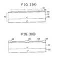
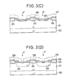
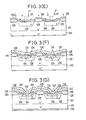
- FIGs. 3 there is shown the second embodiment of the invention.
- the method comprises the steps of epitaxially growing an N-- type monocrystalline silicon layer 121 of low impurity concentration having donor concentration No of about 2 x 10 15 atoms/cm 3 and the thickness of about 15 ⁇ m on a drain substrate 120 of low resistivity comprising an N +- type monocrystalline silicon wafer of high concentration of donor impurities N D of about 1 x 10 18 atoms/cm 3 , thereby to form a drain region 121 of high resistivity, thereafter forming silicon nitride (Si 3 N 4 ) film 123 on the surface of the drain region 121 of high resistivity of a semiconductor wafer 110 through a thin silicon oxide film 122 having the thickness of about 6 x 10 nm (600 A) by a CVD method so that the thickness of the silicon nitrode film 123 is about 10 2 nm (1,000 A), and the removing silicon nitride film 123 except for portions in which well regions functioning as channels are to be formed with resist
- the method comprises the steps growing an silicon oxide film by a thermal oxidation method on the removed portions to form oxide insulating film regions 125 having the thickness of about 1 pm, then removing the silicon nitride films 123 and the resists 124 using phosphoric acid, at the same time removing the thin oxide film 122 located at the lower surface of the silicon nitride film 123, and thereafter forming a silicon oxide insulating film 126 for a gate on the surface of the drain region 121 of high resistivity except for the thick oxide film region 125 by a thermal oxidation method so that the thickness thereof is about 10 2 nm (1,000 A).
- each periphery of the region 125 grows in the upper and lower directions in such a manner as to push up the periphery portion of the silicon nitride film 123. Accordingly, the thick oxide insulating film regions 125 are formed in such a manner that each upper part is projected with respect to the surface of the insulating film 126 for a gate. More particularly, the oxide insulating films 125 are trapezoid-shaped in appearance, which have gradually inclined peripheral edges, respectively.
- the method further comprises the steps of forming a polysilicon film 128 having the thickness of about 4 x 10 2 nm (4,000 A) by a CVD method, selectively removing the polysilicon film by photo-etching techniques with resists 127 serving as a mask so that gate electrodes 128 are left, and injecting boron ions (B + ) into the portions in which there exist no gate electrode 128 on the upper surface of the drain region 121 of high resistivity by an ion implantation method with the gate electrodes 128 serving as a mask.
- the energy for ion implantation is about 60 KeV, and the implanted quantity is about 4 x 10 13 atoms/cm 2 .
- the method further comprises effecting heat treatment for 24 hours at a temperature of about 1,100°C thereby to form well regions 129 having the depth of 5 to 6 ⁇ m by diffusion, and injecting boron ions (B + ) into a predetermined surface of the well regions 129 with the resists 130 (shown with dotted lines) serving as a mask.
- the energy for ion implantation is about 50 KeV, and the implanted quantity if 5 x 10 15 atoms/cm 2 .
- the method further comprises the steps of covering with resists 131 the regions into which the boron ions (B + ) have been injected in the preceding step, and then injecting phosphorus ions (P + ) into the surface of the well region 129 with the resists 131 and the gate electrodes 129 serving as masks.
- a great amount of phosphorus ions (P + ) are immersed into the polysilicon films constituting the gate electrodes 128.
- the energy for ion implantation is about 100 KeV, and the implanted quantity is about 5 x 10 15 atoms/cm 2 .
- the method further comprises the steps of forming an insulating film 132 essentially consisting of phosphoric glass having molecular concentration of about 3% by a CVD method so that the thickness thereof is 7 x 10 2 nm (7,000 A), and effecting heat treatment in the presence of a current of nitrogen at a temperature of about 1,050°C, whereby source regions 133 and well contact regions 134 are formed within the well region 129 by thermal diffusion.
- the method further comprises the steps of opening windows exposed to the surface of the source regions 133 and the well contact region 134 as well as windows for the leading-out port (not shown) of the gate electrodes, then coating aluminum of about 1.5 ⁇ m in thickness by vacuum deposition, thereafter forming source electrode 135 and lead electrodes for a gate (not shown) by etching, coating aluminum having the thickness of 1 ⁇ m on the rear surface of the drain substrate 120 of low resistivity by vacuum deposition, and then effecting heat treatment at a temperature of about 450°C, whereby an alloy drain electrode 136 is formed.
- the vertical-type MOSFET shown in Fig. 3(G) of the second embodiment is completed.
- the peripheral portion of the thick oxide insulating film region 125 rises so as to be gradually sloped surface. Accordingly, when the gate electrode 128, the insulating film 132 and the source electrode 135 are successively stacked, there occurs no crack between respective layers due to the offset structure by the gentle slopes thereof. Further, the stress applied to each films of the layers can become substantially uniform throughout the whole portion of each film.
- another method may be employed, which comprises the steps of effecting arsenic ions (As) implantation with a resist 124 serving as a mask into the surface of the drain region 121 of high resistivity, and then forming a thick oxide insulating film region 125 and then forming a thick oxide insulating film region 125 in the same portions as stated above.
- As arsenic ions
- the arsenic ions (As) thus implanted form an N +- type region of high impurity concentration along the interface between the insulating film region 125 and the drain region 121 of high resistivity by thermal diffusion in Fig. 3(G). Accordingly, similar to the first embodiment, electric currents flow through the N + -type region, thereby making it possible to reduce resistance which originates in the drain region of high resistivity to lessen "ON" resistance in current paths.
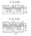
- FIG. 4 there is shown the third embodiment of the invention.
- An example of fabricating processes of an N-channel vertical type MOSFET according to the third embodiment will be described with reference to Figs. 4(A) to 4(H).
- the method comprises the steps of epitaxially growing an N-- type monocrystalline silicon layer of low impurity concentration having donor concentration No of about 2 x 10" atoms/cm 3 and the thickness of about 15 ⁇ m on a drain substrate 220 of low resistivity essentially consisting of an N +- type monocrystalline silicon wafer of high impurity concentration having donor concentration N c of about 1 ⁇ 10 18 atoms/cm 3 thereby to form a drain region 221 of high resistivity, forming a silicon oxide insulating film 222 for a gate on the surface of the drain region 221 of high resistivity of a semiconductor wafer 210 by a thermal oxidation method so that the thickness thereof is about 10 2 nm (1,000 A), thereafter forming a polysilicon film 223 having the thickness of 4 x 10 2 nm (4,000 A) by a CVD method and forming a silicon nitride film (Si 3 N 4 ) 224 on the surface thereof by
- the method further comprises the step of selectively removing the silicon nitride film 224 with resists 225 (shown with dotted lines) serving as masks.
- the removed portions of the film 224 correspond to the portions of the drain region 221 that is to interpose between two well regions and the portions that is to be source regions.
- the method further comprises the step of oxidizing the polysilicon film 223 except for the gate electrode portions by thermal oxidation to change them into silicon oxide films 226.
- the silicon oxide insulating film 226 grows in a manner to push up the opened inner peripheral edge in the window provided in the silicon nitride film 224. Accordingly, the insulating films 226 rise on the surface so as to have trapezoidal shape in cross section.
- the method further comprises the steps of removing the silicon nitride film 224 by photo-etching techniques, selectively removing the polysilicon oxide insulating films 226 which coat the portions in which the well regions will be formed, covering the upper surface of the gate electrodes 223 and the insulating films 226 with resists 227 (shown with dotted line), and injecting boron ions (B + ) into the surface of the drain region 221 of high resistivity by an ion implantation method under the condition that the gate electrode 223 and the resists 227 serve as a mask.
- the energy for ion implantation is about 60 KeV, and the implanted quantity is about 4 x 10 13 atoms/cm 2.
- the method further, comprises the steps of effecting heat treatment for 24 hours at a temperature of 1,100°C to form P well regions 228 by thermal diffusion, and injecting boron ions (B + ) into the surface of the well region 228 from windows opened in the center thereof with the resists 229 serving as masks.
- the energy for ion implantation is about 50 KeV, and the implanted quantity if about 5 x 10 15 atoms/cm 2 .
- the method further comprises the steps of covering the region into which the boron ions are injected at the preceding process with resists 230, and injecting phosphorus ions (P + ) into the well regions 228 with the resist 230, the silicon film 223 and the insulating film 226 serving as a mask.
- phosphorus ions P +
- a great amount of phosphorus ions are entered into the gate electrode 223.
- the energy for ion implantation is about 100 KeV, and the implanted quantity is about 5 x 10 15 atoms/cm 2.
- the method further comprises the steps of forming an insulating film 231 essentially consisting of phosphoric glass, the molecular concentration of phosphorus being about 3%, by a CVD method so that the thickness thereof is 7 x 10 2 cm (7,000 A), and effecting heat treatment in the atmosphere of nitrogen at a temperature of about 1,050°C, whereby source regions 232 and well contact regions 233 are formed within the well region 228 by thermal diffusion.
- the method further comprises the steps of opening windows in the insulating films 222, 231 for forming electrodes on the source regions 232 and well contact regions 233, opening window in the insulating film 231 for leading-out ports of gate electrodes (not shown), coating aluminum on the whole surface thereof by vacuum deposition so that the thickness thereof is 1.5 ⁇ m, forming a source electrode 234, and a lead electrode (not shown), for a gate by etching, thereafter coating aluminum having the thickness of about 1 11m on the whole rear surface of the wafer 210 by vacuum deposition, and alloying it at a temperature of about 450°C thereby to form a drain electrode 235.
- the vertical MOSFET of the third embodiment shown in Fig. 4(H) is completed.
- the oxide insulating film 226 rises so as to be gradual inclined at its surface.
- the insulating film 231 and the source electrode 234 are successively stacked as described above and illustrated in the figures, there occurs no crack between layers due to offset structure by the gentle slopes thereof. Further, the stresses applied to the films of each layers can became substantial uniform as well as the thicknesses thereof.
- another method may be employed, which comprises the steps of injecting an N-type impurity, such as phosphorus ions (P + ) into the silicon polycrystalline 223 with the resists 225 by an ion implantation method in advance.
- an N-type impurity such as phosphorus ions (P + )
- P + phosphorus ions
- the P-type well region is formed on the N-type substrate.
- the present invention is applicable to a P-channel vertical-type MOSFET that an N-type well region is formed on a P-type substrate.
- the vertical-type MOSFET according to the present invention is constituted so as to increase the effective distance between the gate electrode film and the drain region in the central portion of the gate electrode film located between adjacent well regions for forming a channel. Accordingly, this makes it possible to remarkably decrease feedback capacity between the gate and the drain, thereby to effect switching at a high speed.
Landscapes
- Insulated Gate Type Field-Effect Transistor (AREA)
Claims (13)
Applications Claiming Priority (6)
| Application Number | Priority Date | Filing Date | Title |
|---|---|---|---|
| JP25337/83 | 1983-02-17 | ||
| JP25336/83 | 1983-02-17 | ||
| JP58025337A JPS59151467A (ja) | 1983-02-17 | 1983-02-17 | 縦型mosfet |
| JP58025335A JPS59151465A (ja) | 1983-02-17 | 1983-02-17 | 縦型mosfet |
| JP58025336A JPS59151466A (ja) | 1983-02-17 | 1983-02-17 | 縦型mosfet |
| JP25335/83 | 1983-02-17 |
Publications (2)
| Publication Number | Publication Date |
|---|---|
| EP0119400A1 EP0119400A1 (fr) | 1984-09-26 |
| EP0119400B1 true EP0119400B1 (fr) | 1987-08-05 |
Family
ID=27284984
Family Applications (1)
| Application Number | Title | Priority Date | Filing Date |
|---|---|---|---|
| EP84100612A Expired EP0119400B1 (fr) | 1983-02-17 | 1984-01-20 | MOSFET de type vertical et procédé pour sa fabrication |
Country Status (2)
| Country | Link |
|---|---|
| EP (1) | EP0119400B1 (fr) |
| DE (1) | DE3465225D1 (fr) |
Cited By (5)
| Publication number | Priority date | Publication date | Assignee | Title |
|---|---|---|---|---|
| US7910983B2 (en) | 2008-09-30 | 2011-03-22 | Infineon Technologies Austria Ag | MOS transistor having an increased gate-drain capacitance |
| US8030153B2 (en) | 2007-10-31 | 2011-10-04 | Freescale Semiconductor, Inc. | High voltage TMOS semiconductor device with low gate charge structure and method of making |
| CN105225952A (zh) * | 2014-06-10 | 2016-01-06 | 北大方正集团有限公司 | 一种vdmos器件的制作方法及vdmos器件 |
| CN107507860A (zh) * | 2016-06-14 | 2017-12-22 | 株洲中车时代电气股份有限公司 | 倒台面栅igbt结构及其制作方法 |
| CN108110045A (zh) * | 2017-12-18 | 2018-06-01 | 深圳市晶特智造科技有限公司 | 平面型垂直双扩散金属氧化物晶体管及其制作方法 |
Families Citing this family (24)
| Publication number | Priority date | Publication date | Assignee | Title |
|---|---|---|---|---|
| US4571606A (en) * | 1982-06-21 | 1986-02-18 | Eaton Corporation | High density, high voltage power FET |
| JPH04152536A (ja) * | 1990-10-16 | 1992-05-26 | Fuji Electric Co Ltd | Mis型半導体装置の製造方法 |
| JP2962136B2 (ja) * | 1994-03-16 | 1999-10-12 | 株式会社日立製作所 | 絶縁ゲート型半導体装置及びそれを用いた電力変換装置 |
| EP0729186B1 (fr) * | 1995-02-24 | 1999-05-06 | Consorzio per la Ricerca sulla Microelettronica nel Mezzogiorno | Structure intégrée de dispositif de puissance en technologie MOS et procédé pour sa fabrication |
| US5798554A (en) * | 1995-02-24 | 1998-08-25 | Consorzio Per La Ricerca Sulla Microelettronica Nel Mezzogiorno | MOS-technology power device integrated structure and manufacturing process thereof |
| US5869371A (en) * | 1995-06-07 | 1999-02-09 | Stmicroelectronics, Inc. | Structure and process for reducing the on-resistance of mos-gated power devices |
| EP0768714B1 (fr) * | 1995-10-09 | 2003-09-17 | Consorzio per la Ricerca sulla Microelettronica nel Mezzogiorno - CoRiMMe | Méthode de fabrication d'un dispositif de puissance avec anneau de guide profond |
| DE69534919T2 (de) * | 1995-10-30 | 2007-01-25 | Stmicroelectronics S.R.L., Agrate Brianza | Leistungsvorrichtung in MOS-Technologie mit einer einzigen kritischen Größe |
| DE69533134T2 (de) * | 1995-10-30 | 2005-07-07 | Stmicroelectronics S.R.L., Agrate Brianza | Leistungsbauteil hoher Dichte in MOS-Technologie |
| US6228719B1 (en) | 1995-11-06 | 2001-05-08 | Stmicroelectronics S.R.L. | MOS technology power device with low output resistance and low capacitance, and related manufacturing process |
| DE69515876T2 (de) * | 1995-11-06 | 2000-08-17 | Consorzio Per La Ricerca Sulla Microelettronica Nel Mezzogiorno, Catania | Leistungsbauelement in MOS-Technologie mit niedrigem Ausgangswiderstand und geringer Kapazität und dessen Herstellungsverfahren |
| DE69518653T2 (de) * | 1995-12-28 | 2001-04-19 | Consorzio Per La Ricerca Sulla Microelettronica Nel Mezzogiorno, Catania | MOS-Technologie-Leistungsanordnung in integrierter Struktur |
| US6087697A (en) | 1997-10-31 | 2000-07-11 | Stmicroelectronics, Inc. | Radio frequency power MOSFET device having improved performance characteristics |
| US5977588A (en) * | 1997-10-31 | 1999-11-02 | Stmicroelectronics, Inc. | Radio frequency power MOSFET device having improved performance characteristics |
| DE69839439D1 (de) | 1998-05-26 | 2008-06-19 | St Microelectronics Srl | MOS-Technologie-Leistungsanordnung mit hoher Integrationsdichte |
| US6207508B1 (en) | 1999-08-03 | 2001-03-27 | Stmicroelectronics, Inc. | Method for fabricating a radio frequency power MOSFET device having improved performance characteristics |
| US6870221B2 (en) * | 2002-12-09 | 2005-03-22 | Semiconductor Components Industries, Llc | Power switching transistor with low drain to gate capacitance |
| US7067363B2 (en) | 2002-12-30 | 2006-06-27 | Stmicroelectronics S.R.L. | Vertical-conduction and planar-structure MOS device with a double thickness of gate oxide and method for realizing power vertical MOS transistors with improved static and dynamic performances and high scaling down density |
| EP1455397A3 (fr) * | 2002-12-30 | 2005-08-17 | STMicroelectronics S.r.l. | Dispositif MOS vertical et sa méthode de fabrication |
| US20040164346A1 (en) * | 2003-02-20 | 2004-08-26 | Semiconductor Components Industries, Llc. | Power switching transistor with low drain to gate capacitance |
| US7189608B2 (en) | 2003-12-22 | 2007-03-13 | Semiconductor Components Industries, L.L.C. | Semiconductor device having reduced gate charge and reduced on resistance and method |
| WO2007070050A1 (fr) * | 2005-12-14 | 2007-06-21 | Freescale Semiconductor, Inc. | Structure a faible charge de grille pour transistor mos a effet de champ d'alimentation |
| US20090159927A1 (en) | 2007-12-21 | 2009-06-25 | Infineon Technologies Austria Ag | Integrated circuit device and method for its production |
| WO2013128480A1 (fr) * | 2012-02-28 | 2013-09-06 | Stmicroelectronics S.R.L. | Dispositif vertical à semi-conducteur et son processus de fabrication |
Citations (3)
| Publication number | Priority date | Publication date | Assignee | Title |
|---|---|---|---|---|
| EP0077737A2 (fr) * | 1981-10-19 | 1983-04-27 | FAIRCHILD CAMERA & INSTRUMENT CORPORATION | Dispositif à effet de champ à basse capacité |
| WO1983002852A1 (fr) * | 1982-02-09 | 1983-08-18 | Western Electric Co | Thyristor lateral bidirectionnel commande par effet de champ |
| EP0112607A2 (fr) * | 1982-09-03 | 1984-07-04 | Western Electric Company, Incorporated | Transistor MOS de puissance |
Family Cites Families (4)
| Publication number | Priority date | Publication date | Assignee | Title |
|---|---|---|---|---|
| JPS52132684A (en) * | 1976-04-29 | 1977-11-07 | Sony Corp | Insulating gate type field effect transistor |
| IT1133869B (it) * | 1979-10-30 | 1986-07-24 | Rca Corp | Dispositivo mosfet |
| SE456291B (sv) * | 1980-02-22 | 1988-09-19 | Rca Corp | Vertikal mosfet-anordning innefattande en over kollektoromradet belegen skermelektrod for minimering av miller- kapacitansen och stromfortrengningen |
| US4345265A (en) * | 1980-04-14 | 1982-08-17 | Supertex, Inc. | MOS Power transistor with improved high-voltage capability |
-
1984
- 1984-01-20 EP EP84100612A patent/EP0119400B1/fr not_active Expired
- 1984-01-20 DE DE8484100612T patent/DE3465225D1/de not_active Expired
Patent Citations (3)
| Publication number | Priority date | Publication date | Assignee | Title |
|---|---|---|---|---|
| EP0077737A2 (fr) * | 1981-10-19 | 1983-04-27 | FAIRCHILD CAMERA & INSTRUMENT CORPORATION | Dispositif à effet de champ à basse capacité |
| WO1983002852A1 (fr) * | 1982-02-09 | 1983-08-18 | Western Electric Co | Thyristor lateral bidirectionnel commande par effet de champ |
| EP0112607A2 (fr) * | 1982-09-03 | 1984-07-04 | Western Electric Company, Incorporated | Transistor MOS de puissance |
Cited By (6)
| Publication number | Priority date | Publication date | Assignee | Title |
|---|---|---|---|---|
| US8030153B2 (en) | 2007-10-31 | 2011-10-04 | Freescale Semiconductor, Inc. | High voltage TMOS semiconductor device with low gate charge structure and method of making |
| US7910983B2 (en) | 2008-09-30 | 2011-03-22 | Infineon Technologies Austria Ag | MOS transistor having an increased gate-drain capacitance |
| CN105225952A (zh) * | 2014-06-10 | 2016-01-06 | 北大方正集团有限公司 | 一种vdmos器件的制作方法及vdmos器件 |
| CN105225952B (zh) * | 2014-06-10 | 2018-06-15 | 北大方正集团有限公司 | 一种vdmos器件的制作方法及vdmos器件 |
| CN107507860A (zh) * | 2016-06-14 | 2017-12-22 | 株洲中车时代电气股份有限公司 | 倒台面栅igbt结构及其制作方法 |
| CN108110045A (zh) * | 2017-12-18 | 2018-06-01 | 深圳市晶特智造科技有限公司 | 平面型垂直双扩散金属氧化物晶体管及其制作方法 |
Also Published As
| Publication number | Publication date |
|---|---|
| DE3465225D1 (en) | 1987-09-10 |
| EP0119400A1 (fr) | 1984-09-26 |
Similar Documents
| Publication | Publication Date | Title |
|---|---|---|
| EP0119400B1 (fr) | MOSFET de type vertical et procédé pour sa fabrication | |
| US4980306A (en) | Method of making a CMOS device with trench isolation device | |
| KR100415490B1 (ko) | 파워 모스 소자 및 그 제조 방법 | |
| US5849616A (en) | Method of manufacturing a semiconductor device | |
| EP0034910B1 (fr) | Procédé de fabrication d'un dispositif à semi-conducteur et dispositif ainsi obtenu | |
| EP0052450B1 (fr) | Procédé de fabrication d'un dispositif semiconducteur comprenant des électrodes en semiconducteur polycristallin et métal | |
| EP0067206B1 (fr) | Procede de fabrication de dispositifs semi-conducteurs complementaires | |
| US4890142A (en) | Power MOS transistor structure | |
| EP0176747B1 (fr) | Substrat semi-conducteur en silicium à couche isolante enterrée et son procédé de fabrication | |
| US4593459A (en) | Monolithic integrated circuit structure and method of fabrication | |
| EP0083816B1 (fr) | Dispositif semi-conducteur comprenant une configuration d'interconnexion | |
| EP0091984B1 (fr) | Dispositifs à circuits intégrés comprenant des régions d'isolation diélectriques et procédé pour la fabrication de ces dispositifs | |
| US4070687A (en) | Composite channel field effect transistor and method of fabrication | |
| EP0118921A2 (fr) | MOSFET à haute densité d'intégration et à faible résistance à l'état conducteur | |
| JP2002170955A (ja) | 半導体装置およびその製造方法 | |
| US4648909A (en) | Fabrication process employing special masks for the manufacture of high speed bipolar analog integrated circuits | |
| GB2080024A (en) | Semiconductor Device and Method for Fabricating the Same | |
| US5202573A (en) | Dual anode mos scr with anti crosstalk collecting region | |
| US5100814A (en) | Semiconductor device and method of manufacturing the same | |
| EP0337823A2 (fr) | Transistor à effet de champ ayant une tension de claquage élevée | |
| JPH0244154B2 (fr) | ||
| US4942448A (en) | Structure for isolating semiconductor components on an integrated circuit and a method of manufacturing therefor | |
| US4633290A (en) | Monolithic CMOS integrated circuit structure with isolation grooves | |
| JP3402548B2 (ja) | 半導体装置の製造方法 | |
| EP0481965B1 (fr) | Procédé de fabrication des transistors à induction statique à grille isolée formée sur la paroi d'un sillon |
Legal Events
| Date | Code | Title | Description |
|---|---|---|---|
| PUAI | Public reference made under article 153(3) epc to a published international application that has entered the european phase |
Free format text: ORIGINAL CODE: 0009012 |
|
| 17P | Request for examination filed |
Effective date: 19840120 |
|
| AK | Designated contracting states |
Designated state(s): DE FR GB |
|
| RAP1 | Party data changed (applicant data changed or rights of an application transferred) |
Owner name: NISSAN MOTOR CO., LTD. |
|
| 17Q | First examination report despatched |
Effective date: 19860403 |
|
| GRAA | (expected) grant |
Free format text: ORIGINAL CODE: 0009210 |
|
| AK | Designated contracting states |
Kind code of ref document: B1 Designated state(s): DE FR GB |
|
| PG25 | Lapsed in a contracting state [announced via postgrant information from national office to epo] |
Ref country code: FR Free format text: THE PATENT HAS BEEN ANNULLED BY A DECISION OF A NATIONAL AUTHORITY Effective date: 19870805 |
|
| REF | Corresponds to: |
Ref document number: 3465225 Country of ref document: DE Date of ref document: 19870910 |
|
| EN | Fr: translation not filed | ||
| PLBE | No opposition filed within time limit |
Free format text: ORIGINAL CODE: 0009261 |
|
| STAA | Information on the status of an ep patent application or granted ep patent |
Free format text: STATUS: NO OPPOSITION FILED WITHIN TIME LIMIT |
|
| 26N | No opposition filed | ||
| GBPC | Gb: european patent ceased through non-payment of renewal fee | ||
| PG25 | Lapsed in a contracting state [announced via postgrant information from national office to epo] |
Ref country code: DE Effective date: 19881001 |
|
| PG25 | Lapsed in a contracting state [announced via postgrant information from national office to epo] |
Ref country code: GB Free format text: LAPSE BECAUSE OF NON-PAYMENT OF DUE FEES Effective date: 19881122 |