EP0119616A2 - Circuit de retard programmable - Google Patents
Circuit de retard programmable Download PDFInfo
- Publication number
- EP0119616A2 EP0119616A2 EP84102947A EP84102947A EP0119616A2 EP 0119616 A2 EP0119616 A2 EP 0119616A2 EP 84102947 A EP84102947 A EP 84102947A EP 84102947 A EP84102947 A EP 84102947A EP 0119616 A2 EP0119616 A2 EP 0119616A2
- Authority
- EP
- European Patent Office
- Prior art keywords
- input
- delay
- multiplexer
- input port
- port
- Prior art date
- Legal status (The legal status is an assumption and is not a legal conclusion. Google has not performed a legal analysis and makes no representation as to the accuracy of the status listed.)
- Withdrawn
Links
Images


Classifications
-
- H—ELECTRICITY
- H03—ELECTRONIC CIRCUITRY
- H03K—PULSE TECHNIQUE
- H03K3/00—Circuits for generating electric pulses; Monostable, bistable or multistable circuits
- H03K3/02—Generators characterised by the type of circuit or by the means used for producing pulses
- H03K3/027—Generators characterised by the type of circuit or by the means used for producing pulses by the use of logic circuits, with internal or external positive feedback
- H03K3/03—Astable circuits
- H03K3/0315—Ring oscillators
-
- H—ELECTRICITY
- H03—ELECTRONIC CIRCUITRY
- H03K—PULSE TECHNIQUE
- H03K5/00—Manipulating of pulses not covered by one of the other main groups of this subclass
- H03K5/13—Arrangements having a single output and transforming input signals into pulses delivered at desired time intervals
- H03K5/131—Digitally controlled
-
- H—ELECTRICITY
- H03—ELECTRONIC CIRCUITRY
- H03K—PULSE TECHNIQUE
- H03K5/00—Manipulating of pulses not covered by one of the other main groups of this subclass
- H03K2005/00013—Delay, i.e. output pulse is delayed after input pulse and pulse length of output pulse is dependent on pulse length of input pulse
- H03K2005/00078—Fixed delay
- H03K2005/00097—Avoiding variations of delay using feedback, e.g. controlled by a PLL
-
- H—ELECTRICITY
- H03—ELECTRONIC CIRCUITRY
- H03K—PULSE TECHNIQUE
- H03K5/00—Manipulating of pulses not covered by one of the other main groups of this subclass
- H03K2005/00013—Delay, i.e. output pulse is delayed after input pulse and pulse length of output pulse is dependent on pulse length of input pulse
- H03K2005/0015—Layout of the delay element
- H03K2005/00234—Layout of the delay element using circuits having two logic levels
-
- Y—GENERAL TAGGING OF NEW TECHNOLOGICAL DEVELOPMENTS; GENERAL TAGGING OF CROSS-SECTIONAL TECHNOLOGIES SPANNING OVER SEVERAL SECTIONS OF THE IPC; TECHNICAL SUBJECTS COVERED BY FORMER USPC CROSS-REFERENCE ART COLLECTIONS [XRACs] AND DIGESTS
- Y10—TECHNICAL SUBJECTS COVERED BY FORMER USPC
- Y10S—TECHNICAL SUBJECTS COVERED BY FORMER USPC CROSS-REFERENCE ART COLLECTIONS [XRACs] AND DIGESTS
- Y10S331/00—Oscillators
- Y10S331/03—Logic gate active element oscillator
Definitions
- the present invention relates to a delay circuit for delaying a logic signal by a predetermined time which can be digitally programmed.
- timing of logic (digital) signals is very important.
- the delay time of the signal path must be stable in order for the logic circuit to operate properly.
- the delay times of the signal paths must be equal to each other for maintaining the timing relation of the logic signals.
- the correct timing relation of a plurality of logic signals cannot be measured, if the delay time of each signal path is different, i.e. if the skew time of each logic signal is different.
- the delay time of the signal path is not constant and stable, since it depends on the length of the path, the propagation delay times of logic devices (ICs) in the signal path, etc. In particular, the propagation delay times of logic devices are affected by production variations, and vary in accordance with temperature.
- variable delay circuit is necessary to adjust the delay time of the signal path.
- Many variable delay circuits have been proposed, and one of them is shown in FIG. 1.
- Four individual delay devices comprising buffer ICs 12 through 18 are connected in series, and the input of the buffer 12 is connected to the input terminal 10 of the delay circuit.
- Terminal pairs 20 through 28 are connected between the input/output of each buffer and the output terminal 30 of the delay circuit.
- Delay lines may be used for the delay devices instead of buffers 12 through 18.
- the delay time of this variable delay circuit is adjusted by selectively shorting one of terminal pairs 20 through 28. However, it is troublesome to change the delay time frequently, since the previously shorted terminal pair must be opened before shorting another terminal pair.
- Another conventional variable delay circuit employs mechanical switches instead of terminal pairs 20 through 28 of FIG. 1.
- the switches are cumbersome, an the disadvantages of FIG. 1 are not improved.
- a programmable delay circuit comprising a delay device having an input port and an output port, and a multiplexer having a first input port connected to the input port of the delay device, a second input port connected to the output port of the delay device, and an output port, said multiplexer being operative to connect selectively either the first input port or the second input port of the multiplexer to the output port, thereof, whereby the circuit can be programmed and provide delay time from the input port of the delay device to the output port of the multiplexer either including or excluding the propagation delay of the delay device.
- a preferred embodiment of the invention comprises at least one delay device such as a logic gate, buffer and delay line, and a plurality of multiplexers.
- An input multiplexer selects an input logic signal or a feedback logic signal, and the output logic signal therefrom is applied to both the delay device and a direct (non-delay) signal path.
- the output multiplexer selects the delay device or the direct signal path, and a part of the output therefrom is a feedback signal. It should be noted that this feedback is negative.
- the delay time depends on the selection of the output multiplexer. If the output multiplexer selects the delay device, the delay time is the total of the propagation delay times of the delay device and the input and output multiplexers.
- the delay time is the total of the propagation delay times of the input and output multiplexers. Since the multiplexers are controlled by logic signals, the variable delay circuit can be programmed and controlled remotely. When the input multiplexer selects the negative feedback signal (oscillation mode), the variable delay circuit operates as a ring oscillator generating a square wave signal whose period is twice the total delay time of the variable delay circuit. Therefore, the delay time can be measured easily by measuring the frequency or period of the square wave. Additional delay devices and multiplexers may be inserted between the input and output multiplexers for increasing the dealy time selections.
- An input multiplexer 32 selects either an input logic signal at input terminal 10 or a feedback logic signal from an output multiplexer 36 in accordance with a logic control signal CI, and the non-inverted output signal from the mutliplexer 32 is applied to the output multiplexer 36 both directly and through a delay device 34.
- the output multiplexer 36 selects either the delay device 34 or the direct signal path from the input multiplexer 32 in accordance with a logic control signal CO.
- the non-inverted output multiplexer 36 is connected to output terminal 30, and the inverted output thereof is connected to input multiplexer 32 for applying the feedback signal. It should be noted that this feedback is negative, since the delay device is 34 is a non-inverting device.
- the delay device 34 may be a logic gate, buffer, delay line, C-R or L-R network.
- the control signal CI causes the multiplexer 32 to select the input logic signal.
- the delay time of the circuit of FIG. 2 is adjusted by the control signal CO. If the multiplexer 36 selects the delay device 34, the multiplexers 32 and 36 and the delay device 34 are inserted between the input and output terminals 10 and 30, and the delay time is determined by the propagation delay times of the inserted devices. If the multiplexer 36 selects the direct path, only the multiplexers 32 and 36 are inserted between the input and output terminals 10 and 30, and the delay time is determined by the total propagation delay times of the multiplexers 10 and 30.
- the multiplexer 32 selects the feedback signal to form a ring oscillator.
- a square-wave signal is derived at the output terminal 30, and the period thereof is twice the total delay time. Therefore, the actual delay time selected by the control signal CO can be measured easily by measuring the frequency or period of the square-wave signal at the terminal 30.
- the delay circuit of the present invention is programmable and can be controlled remotely. If the delay device 34 is a logic gate or buffer, all components of the present invention can be formed in an IC such as a gate array IC and thereby the programmable delay circuit may be compact in construction.
- the feedback signal may be derived from the output terminal 30, if an inverter is inserted into the feedback path or the delay device 34 is an inverting device.
- FIG. 3 illustrates a second embodiment of the preset invention.
- the delay devices are an AND gate 38, NAND gates 44 and 54, and inverters 42, 48, 50 adn 52.
- the AND gate 38 is inserted between the multiplexers 32 and 40, the inverter 42 and the NAND gate 44 are inserted between the multiplexers 40 and 46, and the inverters 48 through 52 and the NAND gate 54 are inserted between the multiplexers 46 and 36.
- Respective inputs of the gates 38, 44 and 54 are connected to a terminal 56 to receive a disable signal (DISABLE). This disable signal aids in testing the circuit.
- DISABLE disable signal
- the inverting outputs from all the multiplexers are used in order to compensate for differences inpropagation speeds for rising and falling edges of the logic signal.
- the logic level at terminal 56 is normally "High”.
- the control signal CI selects the delay or oscillation mode, and the control signals C0, Cl and C2 adjust the delay time, wherein the signals Cl and CO correspond to the LSB and MSB of the logic control signal respectively. All devices in FIG. 3 may be formed in an IC.
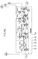
- FIG. 4 illustrates a circuit schematic of a third embodiment of the present invention.
- This embodiment includes three signal delay paths wherein each delay path includes input and output multiplexers 32, 34 and 36, NAND gates 60 through 66 and 70 through 74 operating as delay devices, multiplexers 68, 76, 78 and 80 operating as delay devices, and multiplexers 40, 46 and 58 operating as delay time selectors.
- the NAND 60, 62, 64, 72 and 74 each receive a "High" at one input and thus operate as inverters and multiplexers 68 and 76 each receive a "Low" at the selection terminal S and the input terminal Dl so that they always select the input DO.
- the NAND gates 66 and 70 and multiplexers 78 and 80 receive the disable signal from the terminal 56.
- the disable signal When the disable signal is "High”, the NAND gates 66 and 70 are enabled, and the multiplexers 78 and 80 select the inputs Dl.
- the disable signal When the disable signal is "Low”, the delay paths are off, because the NAND gates 66 and 70 are disabled and the multiplexers 78 and 80 select the input DO.
- the non-inverting output Q of the multiplexer 36-1 is connected to the input Dl of the multiplexer 32-2
- the non-inverting output Q of the multiplexer 36-2 is connected to the input Dl of the multiplexer 32-3
- the non-inverting output Q of the multiplexer 36-3 is connected to the input Dl of the multiplexer 32-1 through the NAND gate (inverter) 82.
- control signal CI selects one of the delay and oscillation modes, and the control signals CO through C3 adjust the delay time, wherein the signals CO and Cl are LSB and MSB of the logic control signal. Since this embodiment employs the NAND gates and multiplexers as delay devices, many combinations of delay times are available.
- the control signal CI is "Low" so that the multiplexers 32 select the input terminals 10.
- each delay path operates independently.
- the delay time is controlled by the signals CO through C3.
- the multiplexers 32 select the inputs Dl and the three delay paths are connected in a single closed loop to form the ring oscillator.
- the frequency or period of the square-wave signal depends on the total delay time of the three delay paths. Since the delay times of the several delay paths are equal to each other and the total delay time is three times the delay time of each individual delay path, the oscillation frequency is low. Thus, it is easy to measure the frequency.
- the FIG. 4 circuit controls the three delay paths in common, but, each delay path may be controlled independently of the others, in which case three logic signals having different skew times can be matched with each other. All the logic devices in FIG. 4 may be formed in an IC.
- the present invention may be used to provide a programmable delay circuit, the delay time of which can be adjusted digitally and remotely. Since the circuit can act as a ring oscillator, it is easy to measure the delay time. Moreover, all components can be formed in an IC.
- latch circuits may be provided for the logic control signals and the disable signal.
Landscapes
- Physics & Mathematics (AREA)
- Nonlinear Science (AREA)
- Pulse Circuits (AREA)
- Stabilization Of Oscillater, Synchronisation, Frequency Synthesizers (AREA)
Applications Claiming Priority (2)
| Application Number | Priority Date | Filing Date | Title |
|---|---|---|---|
| US06/478,606 US4458165A (en) | 1983-03-23 | 1983-03-23 | Programmable delay circuit |
| US478606 | 1983-03-23 |
Publications (2)
| Publication Number | Publication Date |
|---|---|
| EP0119616A2 true EP0119616A2 (fr) | 1984-09-26 |
| EP0119616A3 EP0119616A3 (fr) | 1986-12-30 |
Family
ID=23900608
Family Applications (1)
| Application Number | Title | Priority Date | Filing Date |
|---|---|---|---|
| EP84102947A Withdrawn EP0119616A3 (fr) | 1983-03-23 | 1984-03-16 | Circuit de retard programmable |
Country Status (3)
| Country | Link |
|---|---|
| US (1) | US4458165A (fr) |
| EP (1) | EP0119616A3 (fr) |
| JP (1) | JPS59181819A (fr) |
Cited By (2)
| Publication number | Priority date | Publication date | Assignee | Title |
|---|---|---|---|---|
| EP0244052A3 (en) * | 1986-04-30 | 1989-02-08 | Tektronix, Inc. | Programmable sampling time base circuit |
| FR2695273A1 (fr) * | 1992-08-26 | 1994-03-04 | Nippon Denso Co | Ligne à retard programmable, circuit à retard programmable et oscillateur programmable. |
Families Citing this family (40)
| Publication number | Priority date | Publication date | Assignee | Title |
|---|---|---|---|---|
| US4737670A (en) * | 1984-11-09 | 1988-04-12 | Lsi Logic Corporation | Delay control circuit |
| EP0220454B1 (fr) * | 1985-09-27 | 1990-09-05 | Siemens Aktiengesellschaft | Circuit pour la compensation des variations de temps de propagation de portes en fonction de la température |
| US4626798A (en) * | 1985-12-11 | 1986-12-02 | Gte Laboratories Incorporated | Phase-lock loop including integrated circuit voltage controlled oscillator |
| US4686489A (en) * | 1986-06-16 | 1987-08-11 | Tektronix, Inc. | Triggered voltage controlled oscillator using fast recovery gate |
| US4745310A (en) * | 1986-08-04 | 1988-05-17 | Motorola, Inc. | Programmable delay circuit |
| US5013944A (en) * | 1989-04-20 | 1991-05-07 | International Business Machines Corporation | Programmable delay line utilizing measured actual delays to provide a highly accurate delay |
| US5251228A (en) * | 1989-12-05 | 1993-10-05 | Vlsi Technology, Inc. | Reliability qualification vehicle for application specific integrated circuits |
| US5210450A (en) * | 1990-04-16 | 1993-05-11 | Tektronix, Inc. | Active selectable digital delay circuit |
| US5175452A (en) * | 1991-09-30 | 1992-12-29 | Data Delay Devices, Inc. | Programmable compensated digital delay circuit |
| US5214680A (en) * | 1991-11-01 | 1993-05-25 | Hewlett-Packard Company | CMOS pseudo-NMOS programmable capacitance time vernier and method of calibration |
| US5420467A (en) * | 1992-01-31 | 1995-05-30 | International Business Machines Corporation | Programmable delay clock chopper/stretcher with fast recovery |
| US5389843A (en) * | 1992-08-28 | 1995-02-14 | Tektronix, Inc. | Simplified structure for programmable delays |
| JP2576366B2 (ja) * | 1993-06-23 | 1997-01-29 | 日本電気株式会社 | 可変遅延バッファ回路 |
| US5365204A (en) * | 1993-10-29 | 1994-11-15 | International Business Machines Corporation | CMOS voltage controlled ring oscillator |
| US5621705A (en) * | 1994-05-02 | 1997-04-15 | Colorado Seminary | Programmable timing unit for generating multiple coherent timing signals |
| US5543730A (en) * | 1995-05-17 | 1996-08-06 | Altera Corporation | Techniques for programming programmable logic array devices |
| US5789969A (en) * | 1996-03-15 | 1998-08-04 | Adaptec, Inc. | Digital delay circuit and method |
| US6384630B2 (en) | 1996-06-05 | 2002-05-07 | Altera Corporation | Techniques for programming programmable logic array devices |
| JPH10215156A (ja) * | 1997-01-29 | 1998-08-11 | Nec Corp | 遅延時間可変装置 |
| FR2766275B1 (fr) * | 1997-07-21 | 1999-10-15 | Sgs Thomson Microelectronics | Circuit de validation de modeles de simulation |
| US6137334A (en) | 1998-07-06 | 2000-10-24 | Micron Technology, Inc. | Logic circuit delay stage and delay line utilizing same |
| US6255878B1 (en) * | 1998-09-18 | 2001-07-03 | Lsi Logic Corporation | Dual path asynchronous delay circuit |
| DE10035424A1 (de) * | 2000-07-20 | 2002-01-31 | Infineon Technologies Ag | Zwischenspeichereinrichtung |
| JP2002290217A (ja) * | 2001-03-28 | 2002-10-04 | Fujitsu Ltd | 遅延回路、遅延回路を含む半導体集積回路装置、及び遅延方法 |
| US6650190B2 (en) * | 2001-04-11 | 2003-11-18 | International Business Machines Corporation | Ring oscillator with adjustable delay |
| US6850107B2 (en) | 2001-08-29 | 2005-02-01 | Micron Technology, Inc. | Variable delay circuit and method, and delay locked loop, memory device and computer system using same |
| US7702004B2 (en) * | 2002-12-09 | 2010-04-20 | Alexander Roger Deas | Simultaneous bidirectional differential signalling interface |
| ITMI20040919A1 (it) * | 2004-05-06 | 2004-08-06 | St Microelectronics Srl | Linea di ritardo per circuito oscillatore ad anello |
| ITMI20040918A1 (it) * | 2004-05-06 | 2004-08-06 | St Microelectronics Srl | Circuito oscillatore ad anello |
| EP1643644B1 (fr) * | 2004-09-30 | 2017-07-12 | Infineon Technologies AG | Un circuit à retard avec conversion précise temps-fréquence |
| US7576580B2 (en) * | 2005-04-27 | 2009-08-18 | University Of Connecticut | Energy efficient clock deskew systems and methods |
| US7755402B1 (en) | 2006-04-28 | 2010-07-13 | Nvidia | Calibration of separate delay effects for multiple data strobe signals |
| US7468616B1 (en) * | 2006-08-30 | 2008-12-23 | Xilinx, Inc. | Circuit for and method of generating a delay in an input/output port of an integrated circuit device |
| US8228126B2 (en) * | 2007-04-19 | 2012-07-24 | Mediatek Inc. | Multi-band burst-mode clock and data recovery circuit |
| JP5158764B2 (ja) * | 2007-09-27 | 2013-03-06 | 川崎マイクロエレクトロニクス株式会社 | 位相シフト方法および回路 |
| US9825618B2 (en) * | 2015-01-20 | 2017-11-21 | Mediatek Singapore Pte. Ltd. | Tunable delay circuit and operating method thereof |
| JP6812781B2 (ja) | 2016-12-19 | 2021-01-13 | セイコーエプソン株式会社 | 遅延回路、カウント値生成回路および物理量センサー |
| JP6972660B2 (ja) | 2017-05-29 | 2021-11-24 | セイコーエプソン株式会社 | アイドルトーン分散装置および周波数比計測装置 |
| JP2020072549A (ja) * | 2018-10-31 | 2020-05-07 | 株式会社豊田中央研究所 | 電源装置 |
| US11595032B2 (en) * | 2021-05-27 | 2023-02-28 | Skyworks Solutions, Inc. | Signal delay control using a recirculating delay loop and a phase interpolator |
Family Cites Families (6)
| Publication number | Priority date | Publication date | Assignee | Title |
|---|---|---|---|---|
| US3862406A (en) * | 1973-11-12 | 1975-01-21 | Interstate Electronics Corp | Data reordering system |
| US4017747A (en) * | 1975-08-18 | 1977-04-12 | Rca Corporation | First timing circuit controlled by a second timing circuit for generating long timing intervals |
| US4016511A (en) * | 1975-12-19 | 1977-04-05 | The United States Of America As Represented By The Secretary Of The Air Force | Programmable variable length high speed digital delay line |
| JPS55114018A (en) * | 1979-02-23 | 1980-09-03 | Nippon Telegr & Teleph Corp <Ntt> | Correctable delay unit |
| CH646287A5 (de) * | 1979-09-28 | 1984-11-15 | Siemens Ag Albis | Schaltungsanordnung zur zeitlichen verschiebung von impulsen. |
| JPS5663143U (fr) * | 1979-10-22 | 1981-05-27 |
-
1983
- 1983-03-23 US US06/478,606 patent/US4458165A/en not_active Expired - Fee Related
-
1984
- 1984-03-16 EP EP84102947A patent/EP0119616A3/fr not_active Withdrawn
- 1984-03-23 JP JP59055940A patent/JPS59181819A/ja active Granted
Cited By (2)
| Publication number | Priority date | Publication date | Assignee | Title |
|---|---|---|---|---|
| EP0244052A3 (en) * | 1986-04-30 | 1989-02-08 | Tektronix, Inc. | Programmable sampling time base circuit |
| FR2695273A1 (fr) * | 1992-08-26 | 1994-03-04 | Nippon Denso Co | Ligne à retard programmable, circuit à retard programmable et oscillateur programmable. |
Also Published As
| Publication number | Publication date |
|---|---|
| EP0119616A3 (fr) | 1986-12-30 |
| US4458165A (en) | 1984-07-03 |
| JPH0354898B2 (fr) | 1991-08-21 |
| JPS59181819A (ja) | 1984-10-16 |
Similar Documents
| Publication | Publication Date | Title |
|---|---|---|
| US4458165A (en) | Programmable delay circuit | |
| EP0181047B1 (fr) | Circuit de commande de retard et méthode pour commander les retards dans un élément semi-conducteur | |
| US4504749A (en) | Delay pulse generating circuit | |
| US6469493B1 (en) | Low cost CMOS tester with edge rate compensation | |
| US4489342A (en) | MOSFET Integrated delay circuit for digital signals and its use in color-televison receivers | |
| US5087842A (en) | Delay circuit having one of a plurality of delay lines which may be selected to provide an operation of a ring oscillator | |
| US5459402A (en) | Delay time measuring circuit | |
| JPH06350416A (ja) | デジタルデータ遅延回路 | |
| US6486698B2 (en) | LSI device capable of adjusting the output impedance to match the characteristic impedance | |
| US4527126A (en) | AC parametric circuit having adjustable delay lock loop | |
| KR890017866A (ko) | 필터회로 | |
| KR900002553A (ko) | 위상 검출회로 | |
| US5801562A (en) | Variable delay circuit | |
| MXPA02008946A (es) | Aparato oscilador que se puede probar y controlar para un circuito integrado. | |
| US9059716B1 (en) | Digital PVT compensation for delay chain | |
| US5329240A (en) | Apparatus for measuring clock pulse delay in one or more circuits | |
| JP3522126B2 (ja) | 同期検出方法及び装置、並びに位相同期方法及び装置 | |
| KR19980080257A (ko) | 다중화 회로 | |
| KR100211230B1 (ko) | 열밸런스회로 | |
| JPS5799841A (en) | Automatic signal phase matching circuit | |
| SU641663A1 (ru) | Устройство дл автоматической калибровки | |
| KR0158490B1 (ko) | 프로그래머블 직렬 입출력회로 | |
| JPH03181098A (ja) | フリップフロップ回路 | |
| JPH04265873A (ja) | 遅延時間測定回路付論理回路 | |
| JP2749036B2 (ja) | 位相比較回路 |
Legal Events
| Date | Code | Title | Description |
|---|---|---|---|
| PUAI | Public reference made under article 153(3) epc to a published international application that has entered the european phase |
Free format text: ORIGINAL CODE: 0009012 |
|
| AK | Designated contracting states |
Designated state(s): DE FR GB NL |
|
| PUAL | Search report despatched |
Free format text: ORIGINAL CODE: 0009013 |
|
| AK | Designated contracting states |
Kind code of ref document: A3 Designated state(s): DE FR GB NL |
|
| 17P | Request for examination filed |
Effective date: 19870402 |
|
| 17Q | First examination report despatched |
Effective date: 19880324 |
|
| STAA | Information on the status of an ep patent application or granted ep patent |
Free format text: STATUS: THE APPLICATION IS DEEMED TO BE WITHDRAWN |
|
| 18D | Application deemed to be withdrawn |
Effective date: 19880804 |
|
| RIN1 | Information on inventor provided before grant (corrected) |
Inventor name: JACKSON, RONALD MARK |