EP0220454B1 - Circuit pour la compensation des variations de temps de propagation de portes en fonction de la température - Google Patents
Circuit pour la compensation des variations de temps de propagation de portes en fonction de la température Download PDFInfo
- Publication number
- EP0220454B1 EP0220454B1 EP86112707A EP86112707A EP0220454B1 EP 0220454 B1 EP0220454 B1 EP 0220454B1 EP 86112707 A EP86112707 A EP 86112707A EP 86112707 A EP86112707 A EP 86112707A EP 0220454 B1 EP0220454 B1 EP 0220454B1
- Authority
- EP
- European Patent Office
- Prior art keywords
- differential amplifier
- circuit arrangement
- signal
- multiplexer
- output
- Prior art date
- Legal status (The legal status is an assumption and is not a legal conclusion. Google has not performed a legal analysis and makes no representation as to the accuracy of the status listed.)
- Expired - Lifetime
Links
- 230000003111 delayed effect Effects 0.000 claims abstract description 11
- 230000000295 complement effect Effects 0.000 claims description 3
- 238000011084 recovery Methods 0.000 description 4
- 230000001934 delay Effects 0.000 description 3
- 238000010586 diagram Methods 0.000 description 3
- 230000007704 transition Effects 0.000 description 3
- 239000008186 active pharmaceutical agent Substances 0.000 description 2
- 238000005516 engineering process Methods 0.000 description 1
Images

Classifications
-
- H—ELECTRICITY
- H03—ELECTRONIC CIRCUITRY
- H03K—PULSE TECHNIQUE
- H03K17/00—Electronic switching or gating, i.e. not by contact-making and –breaking
- H03K17/14—Modifications for compensating variations of physical values, e.g. of temperature
-
- H—ELECTRICITY
- H03—ELECTRONIC CIRCUITRY
- H03K—PULSE TECHNIQUE
- H03K17/00—Electronic switching or gating, i.e. not by contact-making and –breaking
- H03K17/51—Electronic switching or gating, i.e. not by contact-making and –breaking characterised by the components used
- H03K17/56—Electronic switching or gating, i.e. not by contact-making and –breaking characterised by the components used by the use, as active elements, of semiconductor devices
- H03K17/60—Electronic switching or gating, i.e. not by contact-making and –breaking characterised by the components used by the use, as active elements, of semiconductor devices the devices being bipolar transistors
- H03K17/603—Electronic switching or gating, i.e. not by contact-making and –breaking characterised by the components used by the use, as active elements, of semiconductor devices the devices being bipolar transistors with coupled emitters
Definitions
- the invention relates to a circuit arrangement according to the preamble of patent claim 1.
- Circuits are therefore usually dimensioned such that phase changes and time differences of signals occurring with increasing temperature can still be tolerated.
- the signal paths are adapted with additional gates so that the same transit times and the same phase changes occur. This cannot compensate for the positive temperature response.
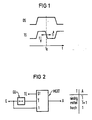
- FIG. 1 shows signal diagrams and the influence of temperature on a time decision to be made by the clock signal.
- the clock is recovered from the data signal DS at the data input of the decision block via internal and external circuits.
- the clock is processed via the clock recovery, filter and amplifier and is passed to the clock input of a decision-maker flip-flop, at whose data input the data signal DS is present.
- Each of the internal and external clock recovery circuits has a positive temperature response. The greater the temperature response of the clock signal path from the data input of the decision module to the clock input of the decision flip-flop, the more the decision time changes with respect to the fixed data signal.
- the decision time t e should be given by the falling edge of the clock signal TS, so this time shifts at lower temperatures in accordance with the faster transit times at earlier points in time, while it increases at higher temperatures due to the longer transit time of the recovered clock signal TS postponed later.
- the invention has for its object to provide a circuit arrangement with a negative temperature response to compensate for the temperature response of gate delays.
- the circuit arrangement according to the invention contains a temperature-controlled multiplexer MUXT and a delay gate GD.
- the temperature-controlled multiplexer MUXT is controlled via a temperature signal at the control input TE.
- the signal to be processed is connected to the signal input E of the circuit arrangement, which is connected directly to the input of the multiplexer corresponding to a logic 1 of the control input TE and via the delay gate DG to the input of the temperature-controlled multiplexer MUXT corresponding to a logic 0 of the control input TE.
- the output A of the circuit arrangement according to the invention is the output of the multiplexer.
- the signal to be processed is now divided up and supplied to the inputs of the temperature-controlled multiplexer MUXT both with and without delay.
- the multiplexer works in such a way that the running time is artificially delayed at low temperatures and the delayed signal is switched to the output. At high temperatures, however, the undelayed signal is switched to the output. In the transition range or in the middle temperature range, the delayed signal is mixed with the undelayed signal and switched to output A.
- This mode of operation is illustrated on the basis of the function table belonging to FIG. 2, which indicates the input of the multiplexer MUXT which is connected to output A as a function of the temperature T.
- the switching of the temperature-controlled multiplexer MUXT is linearized in such a way that it takes place over the entire operating temperature range. Since this area also contains the transition area in which the undelayed and the delayed signal are mixed, only sinusoidal signals can be processed below 500 MHz, but pulses above this frequency.
- the negative temperature response thus results from the fact that the delayed signal is sent to the A output of the multiplexer MUXT in the case of normally fast gate delays and the longer delay in the case of larger gate delays.
- a circuit arrangement according to the invention can therefore lie in the cycle path for the recovery and processing of the cycle.
- Fig. 3 shows a specific embodiment of a circuit according to Fig. 2.
- the circuit is implemented in ECL technology and is connected to the poles VCC and VEE of a supply voltage source.
- the signal to be processed is in complementary form, ie inverted and not inverted at the signal inputs E and E.
- the two signal inputs are connected in parallel to the inputs of two differential amplifiers DV and DV2.
- the collectors of the transistors forming the differential amplifier DV are connected to the positive pole of the supply voltage source VCC via the two load resistors RV1 and RV2.
- the two outputs of the differential amplifier DV are connected to the inputs of a subsequent differential amplifier DV1.
- the respective outputs of the two differential amplifiers DV1 and DV2 are connected in parallel and connected to the positive pole VCC of the supply voltage source via the two load resistors RA1 and RA2.
- the collectors of the transistors of the differential amplifiers DV1 and DV2 assigned to the inverted signal inputs form the signal output A
- the collectors of the respectively assigned transistors of the differential amplifiers DV1 and DV2 connected to the load resistor RA1 form the inverted signal output A.
- the transistor of the differential amplifier DV1 connected to the non-inverted output A is controlled by the output of the transistor of the differential amplifier DV located at the non-inverted signal input E.
- the emitters of the three differential amplifiers DV, DV1 and DV2 are each directly connected to one another.
- the emitters of the differential amplifier DV are connected to the negative pole VEE of the supply voltage source via a current source SV.
- the emitters of the differential amplifier DV1 are connected to the collector of a transistor T1 and the emitters of the differential amplifier DV2 to the collector of a transistor T2.
- the two transistors T1 and T2 form a further differential amplifier, the emitters of which are connected to the negative pole VEE of the supply voltage source via a current source SD.
- a resistor RL is arranged between the emitter of the transistor T1 and the current source SD.
- the series connection of two diodes D1 and D2, a resistor R and a current source S1 is connected between the poles VCC and VEE of the supply voltage source.
- the base of the transistor T1 is connected to the connection point of the resistor R to the current source S1.
- the series connection of a diode D and a current source S2 leads from the connection point of the resistor R to the diode D2 to the pole VEE of the supply voltage source.
- the base of transistor T2 is connected to the connection point of diode D with current source S2.
- the current sources SV, S1, S2 and SD are usually formed by the output circuits of transistors with or without an emitter resistor, the bases of which are controlled by a voltage, preferably a common base voltage.
- the gate formed from the differential amplifier DV is used for signal delay.
- the delay time can be changed using the load resistors RV1 and RV2.
- the delayed signal reaches the input of the differential amplifier DV1, which forms an AND gate with the transistor T1.
- the undelayed signal arrives at the differential amplifier DV2, which together with the transistor T2 is an AND gate.
- Both AND gates realized with series gating are connected to the output via an OR operation in the form of the respective parallel connection of the outputs.
- the thermal switching of the multiplexer is achieved with the help of the opposite voltage temperature responses of the resistor R and the diode D.
- the voltage drop across the resistor R is small and the threshold voltage for the diode is relatively large, so that essentially the transistor T1 conducts and the delayed signal is thus switched to the output A or ⁇ .
- Due to the positive temperature coefficient of the resistor R the voltage drop across the resistor increases with increasing temperature, while at the same time the threshold voltage of the diode D drops due to its negative temperature coefficient. This increasingly switches from transistor T1 to transistor T2 and the undelayed input signal reaches the output via differential amplifier DV2.
- the transition characteristic for the switchover range is linearized using a resistor RL in order to obtain the largest possible temperature range for the switchover.
- the diodes D1 and D2 are used to adapt the voltage level of the series gating stage formed by the transistors T1 and T2 to the potentially higher series gating stage represented by the differential amplifiers DV, DV1 and DV2.
Landscapes
- Amplifiers (AREA)
- Pulse Circuits (AREA)
- Electronic Switches (AREA)
- Logic Circuits (AREA)
- Manipulation Of Pulses (AREA)
Claims (10)
Priority Applications (1)
| Application Number | Priority Date | Filing Date | Title |
|---|---|---|---|
| AT86112707T ATE56326T1 (de) | 1985-09-27 | 1986-09-15 | Schaltungsanordnung zur kompensation des temperaturganges von gatterlaufzeiten. |
Applications Claiming Priority (2)
| Application Number | Priority Date | Filing Date | Title |
|---|---|---|---|
| DE3534561 | 1985-09-27 | ||
| DE3534561 | 1985-09-27 |
Publications (2)
| Publication Number | Publication Date |
|---|---|
| EP0220454A1 EP0220454A1 (fr) | 1987-05-06 |
| EP0220454B1 true EP0220454B1 (fr) | 1990-09-05 |
Family
ID=6282157
Family Applications (1)
| Application Number | Title | Priority Date | Filing Date |
|---|---|---|---|
| EP86112707A Expired - Lifetime EP0220454B1 (fr) | 1985-09-27 | 1986-09-15 | Circuit pour la compensation des variations de temps de propagation de portes en fonction de la température |
Country Status (5)
| Country | Link |
|---|---|
| US (1) | US4758740A (fr) |
| EP (1) | EP0220454B1 (fr) |
| JP (1) | JPS6278910A (fr) |
| AT (1) | ATE56326T1 (fr) |
| DE (1) | DE3673942D1 (fr) |
Families Citing this family (5)
| Publication number | Priority date | Publication date | Assignee | Title |
|---|---|---|---|---|
| US4980586A (en) * | 1987-10-07 | 1990-12-25 | Tektronix, Inc. | Digital integrated circuit propagation delay regulator |
| EP0316607B1 (fr) * | 1987-11-19 | 1992-12-30 | Siemens Aktiengesellschaft | Oscillateur commandé par la tension et déphaseur intégré monolithique à semi-conducteurs |
| DE4110340C2 (de) * | 1990-04-16 | 1993-11-25 | Tektronix Inc | Aktive ansteuerbare digitale Verzögerungsschaltung |
| US6082177A (en) * | 1997-09-22 | 2000-07-04 | Snap-On Tools Company | Nitric oxide enhanced response circuit for gas analyzer |
| US7453302B2 (en) * | 2003-12-23 | 2008-11-18 | Infineon Technologies Ag | Temperature compensated delay signals |
Family Cites Families (11)
| Publication number | Priority date | Publication date | Assignee | Title |
|---|---|---|---|---|
| US3576468A (en) * | 1967-01-04 | 1971-04-27 | Automation Ind Inc | Stroboscope control system |
| US3515998A (en) * | 1967-12-08 | 1970-06-02 | Ibm | Real-time detection of latch resolution using threshold means |
| US3769528A (en) * | 1972-12-27 | 1973-10-30 | Ibm | Low power fet driver circuit |
| DE2723386C3 (de) * | 1976-06-01 | 1981-08-13 | Motorola, Inc., 60196 Schaumburg, Ill. | Logik Schaltungsanordnung |
| DE2855724A1 (de) * | 1978-12-22 | 1980-07-03 | Ibm Deutschland | Verfahren und vorrichtung zur angleichung der unterschiedlichen signalverzoegerungszeiten von halbleiterchips |
| JPS6042659B2 (ja) * | 1980-07-17 | 1985-09-24 | テクトロニクス・インコ−ポレイテツド | スイツチ回路 |
| JPS58114622A (ja) * | 1981-12-28 | 1983-07-08 | Fujitsu Ltd | 遅延回路 |
| FR2519211A1 (fr) * | 1981-12-30 | 1983-07-01 | Radiotechnique Compelec | Etage de sortie pour circuit integre a reseau de portes de la technique ecl regule vis-a-vis des variations liees aux temperatures de fonctionnement |
| US4458165A (en) * | 1983-03-23 | 1984-07-03 | Tektronix, Inc. | Programmable delay circuit |
| US4593205A (en) * | 1983-07-01 | 1986-06-03 | Motorola, Inc. | Macrocell array having an on-chip clock generator |
| US4641048A (en) * | 1984-08-24 | 1987-02-03 | Tektronix, Inc. | Digital integrated circuit propagation delay time controller |
-
1986
- 1986-09-15 DE DE8686112707T patent/DE3673942D1/de not_active Expired - Lifetime
- 1986-09-15 AT AT86112707T patent/ATE56326T1/de not_active IP Right Cessation
- 1986-09-15 EP EP86112707A patent/EP0220454B1/fr not_active Expired - Lifetime
- 1986-09-24 JP JP61225762A patent/JPS6278910A/ja active Pending
- 1986-09-29 US US06/913,410 patent/US4758740A/en not_active Expired - Fee Related
Also Published As
| Publication number | Publication date |
|---|---|
| JPS6278910A (ja) | 1987-04-11 |
| ATE56326T1 (de) | 1990-09-15 |
| EP0220454A1 (fr) | 1987-05-06 |
| DE3673942D1 (de) | 1990-10-11 |
| US4758740A (en) | 1988-07-19 |
Similar Documents
| Publication | Publication Date | Title |
|---|---|---|
| DE69427667T2 (de) | Differenz-Abtast- und Halteschaltung | |
| DE3883323T2 (de) | Ausgangspufferschaltungen. | |
| DE2555297C2 (de) | Digitalschaltung mit Feldeffekttransistoren | |
| DE69122189T2 (de) | Flip-Flop-Schaltung vom "Master-Slave"-Typ | |
| DE68919021T2 (de) | Zweipegel-ECL-Multiplexer ohne gemeinsame Emitterpille. | |
| DE69202157T2 (de) | Lasertreiber zur Verwendung in einem optischen Plattenlaufwerk. | |
| DE68917111T2 (de) | BICMOS-Treiberschaltung für CMOS-logische Schaltungen hoher Dichte. | |
| DE4140564A1 (de) | Pulssignalgenerator und zugeordnete kaskodeschaltung | |
| DE3854319T2 (de) | ECL/TTL-Pegelumsetzer mit TTL Tri-State Ausgang und ECL Steuereingang. | |
| EP0220454B1 (fr) | Circuit pour la compensation des variations de temps de propagation de portes en fonction de la température | |
| DE68919447T2 (de) | Bei schwacher Betriebsspannung betreibbare logische Schaltung. | |
| DE2944034C2 (de) | Flip-Flop-Schaltung sowie damit ausgerüstete Frequenzteilerschaltung | |
| EP0360888B1 (fr) | Modulateur CMOS d'impulsions en durée | |
| DE1807219C3 (de) | J-K-Master- Slave Flip-Flop | |
| DE68925799T2 (de) | Einen metastabilen Zustand zulassende Kippschaltung | |
| DE1537379A1 (de) | Sicherheitsschaltung zum Durchfuehren logischer Verknuepfungen,insbesondere fuer das Eisenbahnsicherungswesen | |
| DE3501274A1 (de) | Schalter | |
| DE69107432T2 (de) | Einstellbare Verzögerungsanordnung. | |
| DE68924426T2 (de) | Selbstreferenzierte Stromschaltungslogik mit Push-Pull-Ausgangspuffer. | |
| DE1512513A1 (de) | Bistabile logische Schaltung | |
| EP0371163B1 (fr) | Circuit de retard pour signaux impulsionnels, pouvant être intégré | |
| DE2027991C3 (de) | Mehrstufige bistabile Kippschaltung | |
| DE3783436T2 (de) | Transistor-transistor-logikschaltung mit internen verzoegerungsgliedern. | |
| DE69735075T2 (de) | Verzögerungsschaltkreis | |
| EP0448744A1 (fr) | Circuit de synchronisation d'horloge |
Legal Events
| Date | Code | Title | Description |
|---|---|---|---|
| PUAI | Public reference made under article 153(3) epc to a published international application that has entered the european phase |
Free format text: ORIGINAL CODE: 0009012 |
|
| AK | Designated contracting states |
Kind code of ref document: A1 Designated state(s): AT DE FR GB IT NL |
|
| 17P | Request for examination filed |
Effective date: 19871102 |
|
| 17Q | First examination report despatched |
Effective date: 19900212 |
|
| GRAA | (expected) grant |
Free format text: ORIGINAL CODE: 0009210 |
|
| PGFP | Annual fee paid to national office [announced via postgrant information from national office to epo] |
Ref country code: AT Payment date: 19900830 Year of fee payment: 5 |
|
| AK | Designated contracting states |
Kind code of ref document: B1 Designated state(s): AT DE FR GB IT NL |
|
| REF | Corresponds to: |
Ref document number: 56326 Country of ref document: AT Date of ref document: 19900915 Kind code of ref document: T |
|
| REF | Corresponds to: |
Ref document number: 3673942 Country of ref document: DE Date of ref document: 19901011 |
|
| ET | Fr: translation filed | ||
| ITF | It: translation for a ep patent filed | ||
| GBT | Gb: translation of ep patent filed (gb section 77(6)(a)/1977) | ||
| PLBE | No opposition filed within time limit |
Free format text: ORIGINAL CODE: 0009261 |
|
| STAA | Information on the status of an ep patent application or granted ep patent |
Free format text: STATUS: NO OPPOSITION FILED WITHIN TIME LIMIT |
|
| 26N | No opposition filed | ||
| PG25 | Lapsed in a contracting state [announced via postgrant information from national office to epo] |
Ref country code: AT Effective date: 19910915 |
|
| ITTA | It: last paid annual fee | ||
| PGFP | Annual fee paid to national office [announced via postgrant information from national office to epo] |
Ref country code: GB Payment date: 19940815 Year of fee payment: 9 |
|
| PGFP | Annual fee paid to national office [announced via postgrant information from national office to epo] |
Ref country code: FR Payment date: 19940920 Year of fee payment: 9 |
|
| PGFP | Annual fee paid to national office [announced via postgrant information from national office to epo] |
Ref country code: NL Payment date: 19940930 Year of fee payment: 9 |
|
| PGFP | Annual fee paid to national office [announced via postgrant information from national office to epo] |
Ref country code: DE Payment date: 19941118 Year of fee payment: 9 |
|
| PG25 | Lapsed in a contracting state [announced via postgrant information from national office to epo] |
Ref country code: GB Effective date: 19950915 |
|
| PG25 | Lapsed in a contracting state [announced via postgrant information from national office to epo] |
Ref country code: NL Effective date: 19960401 |
|
| GBPC | Gb: european patent ceased through non-payment of renewal fee |
Effective date: 19950915 |
|
| PG25 | Lapsed in a contracting state [announced via postgrant information from national office to epo] |
Ref country code: FR Effective date: 19960531 |
|
| PG25 | Lapsed in a contracting state [announced via postgrant information from national office to epo] |
Ref country code: DE Effective date: 19960601 |
|
| NLV4 | Nl: lapsed or anulled due to non-payment of the annual fee |
Effective date: 19960401 |
|
| REG | Reference to a national code |
Ref country code: FR Ref legal event code: ST |
|
| PG25 | Lapsed in a contracting state [announced via postgrant information from national office to epo] |
Ref country code: IT Free format text: LAPSE BECAUSE OF NON-PAYMENT OF DUE FEES;WARNING: LAPSES OF ITALIAN PATENTS WITH EFFECTIVE DATE BEFORE 2007 MAY HAVE OCCURRED AT ANY TIME BEFORE 2007. THE CORRECT EFFECTIVE DATE MAY BE DIFFERENT FROM THE ONE RECORDED. Effective date: 20050915 |