EP0120389A2 - Verfahren zur Steuerung eines Halbleiterlasers - Google Patents
Verfahren zur Steuerung eines Halbleiterlasers Download PDFInfo
- Publication number
- EP0120389A2 EP0120389A2 EP84102694A EP84102694A EP0120389A2 EP 0120389 A2 EP0120389 A2 EP 0120389A2 EP 84102694 A EP84102694 A EP 84102694A EP 84102694 A EP84102694 A EP 84102694A EP 0120389 A2 EP0120389 A2 EP 0120389A2
- Authority
- EP
- European Patent Office
- Prior art keywords
- laser
- current
- semiconductor laser
- high frequency
- noise
- Prior art date
- Legal status (The legal status is an assumption and is not a legal conclusion. Google has not performed a legal analysis and makes no representation as to the accuracy of the status listed.)
- Granted
Links
- 239000004065 semiconductor Substances 0.000 title claims abstract description 21
- 238000000034 method Methods 0.000 title claims description 11
- 230000010355 oscillation Effects 0.000 claims abstract description 15
- 230000003287 optical effect Effects 0.000 claims description 10
- 238000010586 diagram Methods 0.000 description 5
- 230000000694 effects Effects 0.000 description 4
- 239000003990 capacitor Substances 0.000 description 1
- 230000008878 coupling Effects 0.000 description 1
- 238000010168 coupling process Methods 0.000 description 1
- 238000005859 coupling reaction Methods 0.000 description 1
- 230000010365 information processing Effects 0.000 description 1
- 230000003595 spectral effect Effects 0.000 description 1
- 239000000758 substrate Substances 0.000 description 1
- 230000001629 suppression Effects 0.000 description 1
Images



Classifications
-
- H—ELECTRICITY
- H01—ELECTRIC ELEMENTS
- H01S—DEVICES USING THE PROCESS OF LIGHT AMPLIFICATION BY STIMULATED EMISSION OF RADIATION [LASER] TO AMPLIFY OR GENERATE LIGHT; DEVICES USING STIMULATED EMISSION OF ELECTROMAGNETIC RADIATION IN WAVE RANGES OTHER THAN OPTICAL
- H01S3/00—Lasers, i.e. devices using stimulated emission of electromagnetic radiation in the infrared, visible or ultraviolet wave range
-
- G—PHYSICS
- G11—INFORMATION STORAGE
- G11B—INFORMATION STORAGE BASED ON RELATIVE MOVEMENT BETWEEN RECORD CARRIER AND TRANSDUCER
- G11B7/00—Recording or reproducing by optical means, e.g. recording using a thermal beam of optical radiation by modifying optical properties or the physical structure, reproducing using an optical beam at lower power by sensing optical properties; Record carriers therefor
- G11B7/12—Heads, e.g. forming of the optical beam spot or modulation of the optical beam
- G11B7/125—Optical beam sources therefor, e.g. laser control circuitry specially adapted for optical storage devices; Modulators, e.g. means for controlling the size or intensity of optical spots or optical traces
- G11B7/126—Circuits, methods or arrangements for laser control or stabilisation
-
- G—PHYSICS
- G11—INFORMATION STORAGE
- G11B—INFORMATION STORAGE BASED ON RELATIVE MOVEMENT BETWEEN RECORD CARRIER AND TRANSDUCER
- G11B7/00—Recording or reproducing by optical means, e.g. recording using a thermal beam of optical radiation by modifying optical properties or the physical structure, reproducing using an optical beam at lower power by sensing optical properties; Record carriers therefor
- G11B7/12—Heads, e.g. forming of the optical beam spot or modulation of the optical beam
- G11B7/13—Optical detectors therefor
-
- H—ELECTRICITY
- H01—ELECTRIC ELEMENTS
- H01S—DEVICES USING THE PROCESS OF LIGHT AMPLIFICATION BY STIMULATED EMISSION OF RADIATION [LASER] TO AMPLIFY OR GENERATE LIGHT; DEVICES USING STIMULATED EMISSION OF ELECTROMAGNETIC RADIATION IN WAVE RANGES OTHER THAN OPTICAL
- H01S5/00—Semiconductor lasers
- H01S5/06—Arrangements for controlling the laser output parameters, e.g. by operating on the active medium
- H01S5/062—Arrangements for controlling the laser output parameters, e.g. by operating on the active medium by varying the potential of the electrodes
- H01S5/06209—Arrangements for controlling the laser output parameters, e.g. by operating on the active medium by varying the potential of the electrodes in single-section lasers
- H01S5/06216—Pulse modulation or generation
-
- H—ELECTRICITY
- H01—ELECTRIC ELEMENTS
- H01S—DEVICES USING THE PROCESS OF LIGHT AMPLIFICATION BY STIMULATED EMISSION OF RADIATION [LASER] TO AMPLIFY OR GENERATE LIGHT; DEVICES USING STIMULATED EMISSION OF ELECTROMAGNETIC RADIATION IN WAVE RANGES OTHER THAN OPTICAL
- H01S5/00—Semiconductor lasers
- H01S5/06—Arrangements for controlling the laser output parameters, e.g. by operating on the active medium
- H01S5/065—Mode locking; Mode suppression; Mode selection ; Self pulsating
- H01S5/0651—Mode control
- H01S5/0653—Mode suppression, e.g. specific multimode
- H01S5/0654—Single longitudinal mode emission
Definitions
- the present invention relates to a method of driving a semiconductor laser, and more particularly to a driving method which suppresses laser noise in the case of employing a semiconductor laser as an information processing light source.
- Semiconductor lasers are being put into practical use as pickup light sources for an optical video disc, an optical digital audio disc, etc. Since, however, the coherency of the semiconductor laser is too good, there is the problem that the laser output fluctuates due to the feedback of reflected light from an external optical system. Laser noise attributed to the feedback of the reflected light develops conspicuously in a semiconductor laser which oscillates in single mode under direct-current drive. Further, the single mode laser has the problem that, even when the feedback of reflected light is not involved, two or more modes oscillate competitively within a certain temperature range, to increase laser noise.
- An object of the present invention is to provide a method of driving a semiconductor laser which is remarkably effective to suppress even laser noise attendant upon a temperature change by means of the high frequency superposition-laser drive.
- the present invention for accomplishing such object is characterized in that a semiconductor laser oscillating in a single mode under direct-current drive is driven by a signal with a high frequency current superposed on a direct current, so as to be brought into continuous wave pulsed oscillation at a pulse width of at most 1.2 ns.
- Figure 1 is a diagram illustrative of an example of a circuit arrangement for performing the present invention.
- a semiconductor laser 1 is driven by the superposed currents of a direct current source 2 and a high frequency current source 3.
- Letters L and C in Figure 1 denote a coil and a capacitor, respectively, which are inserted so as to permit the two current sources to drive the semiconductor laser independently.
- the semiconductor laser 1 as an information playback light source, the laser beam from the semiconductor laser 1 is guided to a recording medium and condensed as a minute light spot by optical means such as lenses.
- Figure 2(a) is a diagram showing the current - optical output characteristic of the semiconductor laser.
- the laser is driven by a current I in which the direct current I and the high frequency current ⁇ I ⁇ cos (2 ⁇ f t):
- Figure 2(b) shows the time variation-of the laser driving current.
- I th denotes the oscillation threshold current
- L 0 and ⁇ L denote the D.C. light output and A.C. light output corresponding to I 0 and ⁇ I, respectively.
- the laser oscillates only when the laser driving current I exceeds I th , so that the laser output L becomes a continuous wave pulsed oscillation.
- the high frequency current is set at a sufficiently large amplitude so that the laser oscillation may be turned “on” and “off” at the high frequency as described above. Even in a semiconductor laser having a uniform spectral spread, several longitudinal modes oscillate at the rise of laser oscillation. In contrast, when the laser oscillation is turned “on” and “off” at the high frequency as described above, a multiple longitudinal mode oscillation state is held, and the continuous wave pulsed oscillation is established.
- the high frequency current is defined by the frequency f and the amplitude ⁇ I, while the continuous wave pulses are defined by a pulse repetition frequency f and a modulation depth ⁇ :
- L m denotes the average optical output during the modulation.
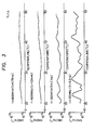
- Figure 3 shows the temperature variation of laser noise in the absence of feedback of reflected light.
- the laser noise is indicated by RIll (Relative Intensity Noise):
- i N and i DC denote noise current and direct current in the case of photoelectrically converting and detecting the emergent light of the laser by means of a photodetector, respectively
- ⁇ f denotes the measured bandwidth of the noise current.
- the RIN shown in Figure 3 is at 8 MHz which is the signal frequency of an optical video disc.
- f is taken on the axis of abscissas, while the changing magnitudes of the RINs at temperatures of 20 °C - 50 °C are represented on the axis of ordinates.
- Each solid line corresponds to the case of Figure 3 where no reflected light was fed back.
- the RINs are indicated as their changing magnitudes in the temperature range of 20 °C- 50 °C. It is understood that, for ⁇ not smaller than 1.2 or for ⁇ not greater than 1.15 ns, the RIN values are small, stable against temperature changes and scarecely affected by the feedback - of reflected light.
- the noise suppressing effect is greater as f is higher and ⁇ is greater.
- ⁇ is greater.
- the upper limit of the pulse width at which the noise suppressing effect becomes particularly remarkable is given from Equation (4) as follows in correspondence with f ⁇ 550 MHz and ⁇ ⁇ 1.2: ns
- the upper limit of f is approximately 4 GHz in view of the modulation characteristic of the laser, and the upper limit of ⁇ is approximately 3 in view of the present-day technique of a high frequency oscillator circuit.
- the lower limit of-the light pulse width corresponding to these values is given from Equation (4) as follows: ns To sum up, the effect of suppressing laser noise becomes especially remarkable in such a way that the laser is brought into multiple mode oscillation by performing high frequency modulation so as to render the pulse width Z at most 1.2 ns.
- the present invention can provide a semiccnductor laser whose noise level is low and stable against temperatures and is scarcely affected by the feedback of reflected light. Therefore, an information playback apparatus of high quality can be provided by employing the semiconductor laser according to the present invention as a light source for information playback.
Landscapes
- Physics & Mathematics (AREA)
- Optics & Photonics (AREA)
- Electromagnetism (AREA)
- Condensed Matter Physics & Semiconductors (AREA)
- General Physics & Mathematics (AREA)
- Engineering & Computer Science (AREA)
- Plasma & Fusion (AREA)
- Semiconductor Lasers (AREA)
- Optical Head (AREA)
Applications Claiming Priority (2)
| Application Number | Priority Date | Filing Date | Title |
|---|---|---|---|
| JP44230/83 | 1983-03-18 | ||
| JP58044230A JPS59171037A (ja) | 1983-03-18 | 1983-03-18 | 半導体レーザの駆動方法及び駆動装置 |
Publications (3)
| Publication Number | Publication Date |
|---|---|
| EP0120389A2 true EP0120389A2 (de) | 1984-10-03 |
| EP0120389A3 EP0120389A3 (en) | 1985-04-24 |
| EP0120389B1 EP0120389B1 (de) | 1987-09-09 |
Family
ID=12685730
Family Applications (1)
| Application Number | Title | Priority Date | Filing Date |
|---|---|---|---|
| EP84102694A Expired EP0120389B1 (de) | 1983-03-18 | 1984-03-12 | Verfahren zur Steuerung eines Halbleiterlasers |
Country Status (5)
| Country | Link |
|---|---|
| US (1) | US4712218A (de) |
| EP (1) | EP0120389B1 (de) |
| JP (1) | JPS59171037A (de) |
| KR (1) | KR910003217B1 (de) |
| DE (1) | DE3466141D1 (de) |
Cited By (7)
| Publication number | Priority date | Publication date | Assignee | Title |
|---|---|---|---|---|
| FR2595857A1 (fr) * | 1986-03-17 | 1987-09-18 | Pioneer Electronic Corp | Appareil d'enregistrement et de reproduction de donnees optiques |
| EP0189295A3 (de) * | 1985-01-22 | 1988-07-20 | Sharp Kabushiki Kaisha | Modulationsverfahren für einen Halbleiterlaser |
| FR2683401A1 (fr) * | 1991-10-31 | 1993-05-07 | Alcatel Nv | Generateur optique, notamment pour le transport d'un signal hyperfrequence. |
| EP0551121A1 (de) * | 1992-01-10 | 1993-07-14 | Fujitsu Limited | Stromversorgungsgerät für eine Halbleiterlichtquelle mit optimierter Einstellung für den Betrieb einer Laserdiode |
| EP0645766A1 (de) * | 1993-09-29 | 1995-03-29 | Sony Corporation | Aufzeichnungs- und/oder Wiedergabevorrichtung für magnetooptisches Medium |
| KR970023243A (ko) * | 1995-10-16 | 1997-05-30 | 이데이 노부유키 | 반도체 레이저 소자의 출력 제어장치 |
| WO2000039793A1 (en) * | 1998-12-24 | 2000-07-06 | Koninklijke Philips Electronics N.V. | Optical recording/reproducing device having a system for the reduction of laser noise when reading data from the record carrier |
Families Citing this family (16)
| Publication number | Priority date | Publication date | Assignee | Title |
|---|---|---|---|---|
| JPH0743841B2 (ja) * | 1985-06-25 | 1995-05-15 | シャープ株式会社 | 半導体レ−ザ駆動方法 |
| US4799069A (en) * | 1986-04-18 | 1989-01-17 | Minolta Camera Kabushiki Kaisha | Laser recording apparatus |
| JPH03227585A (ja) * | 1989-10-30 | 1991-10-08 | Minolta Camera Co Ltd | レ−ザ光源ユニット |
| US5065401A (en) * | 1991-02-26 | 1991-11-12 | Spectra Diode Laboratories, Inc. | Pulse jitter reduction method for a laser diode or array |
| JPH0589465A (ja) * | 1991-06-28 | 1993-04-09 | Hitachi Ltd | 光学式情報記録再生方法およびその装置 |
| JP3045357B2 (ja) * | 1992-07-28 | 2000-05-29 | 富士写真フイルム株式会社 | 光走査記録装置 |
| US5309461A (en) * | 1992-07-29 | 1994-05-03 | International Business Machines Corporation | Compensated laser drive circuit |
| DE19607880C2 (de) * | 1996-03-01 | 1998-01-22 | Agfa Gevaert Ag | Verfahren und Schaltung zum Betrieb einer Laserdiode |
| JP3780650B2 (ja) * | 1997-08-05 | 2006-05-31 | ソニー株式会社 | 半導体レーザの平均光出力の設定方法および半導体レーザの高周波電流の重畳条件の設定方法 |
| JPH11121871A (ja) * | 1997-10-15 | 1999-04-30 | Fujitsu Ltd | ペルチェ素子を有するモジュール |
| EP1341164A3 (de) * | 2002-02-21 | 2004-12-01 | Mitsumi Electric Co., Ltd. | Vorrichtung zur Steuerung des Pegels der optischen Leistung zur Stabilisierung der Oszillation in einer Laserdiode |
| US20080212455A1 (en) * | 2004-05-25 | 2008-09-04 | Koninklijke Philips Electronics, N.V. | Method of Enhancing Laser Operating Efficiency |
| JP2006303332A (ja) * | 2005-04-22 | 2006-11-02 | Ricoh Opt Ind Co Ltd | 光源装置およびそれを用いた光ピックアップ装置、光ビーム走査装置 |
| US7873085B2 (en) * | 2007-10-23 | 2011-01-18 | Andrei Babushkin | Method and device for controlling optical output of laser diode |
| US8750341B2 (en) * | 2008-01-04 | 2014-06-10 | Mindspeed Technologies, Inc. | Method and apparatus for reducing optical signal speckle |
| US20120250707A1 (en) * | 2011-03-31 | 2012-10-04 | Electro Scientific Industries, Inc. | Stabilization of pulsed mode seed lasers |
Family Cites Families (9)
| Publication number | Priority date | Publication date | Assignee | Title |
|---|---|---|---|---|
| US3577018A (en) * | 1968-03-15 | 1971-05-04 | Nippon Electric Co | High-speed logic device employing a gunn-effect element and a semiconductor laser element |
| US3614447A (en) * | 1969-06-16 | 1971-10-19 | Bell Telephone Labor Inc | Method for modulating semiconductor lasers |
| US3641459A (en) * | 1969-06-16 | 1972-02-08 | Bell Telephone Labor Inc | Apparatus and method for narrowing the pulse width and stabilizing the repetition rate in semiconductor lasers exhibiting self-induced pulsing |
| US4243952A (en) * | 1978-10-30 | 1981-01-06 | Rca Corporation | Temperature compensated bias circuit for semiconductor lasers |
| NL8004159A (nl) * | 1979-08-03 | 1981-01-22 | Hitachi Ltd | Optische opneeminrichting. |
| JPS599086B2 (ja) * | 1980-08-20 | 1984-02-29 | 株式会社日立製作所 | 光学的情報再生装置 |
| JPS57128089A (en) * | 1981-01-31 | 1982-08-09 | Nippon Telegr & Teleph Corp <Ntt> | Driving circuit for semiconductor laser |
| US4484331A (en) * | 1981-07-20 | 1984-11-20 | Rca Corporation | Regulator for bias current of semiconductor laser diode |
| US4485475A (en) * | 1983-05-27 | 1984-11-27 | The Mitre Corporation | Optical source peak wavelength control using a wavelength feedback network |
-
1983
- 1983-03-18 JP JP58044230A patent/JPS59171037A/ja active Granted
-
1984
- 1984-03-09 KR KR1019840001197A patent/KR910003217B1/ko not_active Expired
- 1984-03-12 DE DE8484102694T patent/DE3466141D1/de not_active Expired
- 1984-03-12 EP EP84102694A patent/EP0120389B1/de not_active Expired
- 1984-03-19 US US06/590,871 patent/US4712218A/en not_active Expired - Lifetime
Cited By (12)
| Publication number | Priority date | Publication date | Assignee | Title |
|---|---|---|---|---|
| EP0189295A3 (de) * | 1985-01-22 | 1988-07-20 | Sharp Kabushiki Kaisha | Modulationsverfahren für einen Halbleiterlaser |
| FR2595857A1 (fr) * | 1986-03-17 | 1987-09-18 | Pioneer Electronic Corp | Appareil d'enregistrement et de reproduction de donnees optiques |
| FR2683401A1 (fr) * | 1991-10-31 | 1993-05-07 | Alcatel Nv | Generateur optique, notamment pour le transport d'un signal hyperfrequence. |
| EP0541420A1 (de) * | 1991-10-31 | 1993-05-12 | Alcatel N.V. | Optischer Generator zur Übertragung eines Mikrowellensignals |
| US5311531A (en) * | 1991-10-31 | 1994-05-10 | Alcatel N.V. | Light generator, in particular for conveying a microwave signal |
| EP0551121A1 (de) * | 1992-01-10 | 1993-07-14 | Fujitsu Limited | Stromversorgungsgerät für eine Halbleiterlichtquelle mit optimierter Einstellung für den Betrieb einer Laserdiode |
| US5987044A (en) * | 1992-01-10 | 1999-11-16 | Fujitsu Limited | Semiconductor light source system having an optimized setting for driving a laser diode |
| EP0645766A1 (de) * | 1993-09-29 | 1995-03-29 | Sony Corporation | Aufzeichnungs- und/oder Wiedergabevorrichtung für magnetooptisches Medium |
| US5495456A (en) * | 1993-09-29 | 1996-02-27 | Sony Corporation | Magneto-optical recording and reproducing apparatus having a laser driving circuit which superimposes a signal having a frequency at least double the maximum recording signal frequency |
| KR970023243A (ko) * | 1995-10-16 | 1997-05-30 | 이데이 노부유키 | 반도체 레이저 소자의 출력 제어장치 |
| WO2000039793A1 (en) * | 1998-12-24 | 2000-07-06 | Koninklijke Philips Electronics N.V. | Optical recording/reproducing device having a system for the reduction of laser noise when reading data from the record carrier |
| US6414919B1 (en) | 1998-12-24 | 2002-07-02 | Koninklijke Philips Electronics N.V. | Device having a first operational state for writing information onto a record carrier |
Also Published As
| Publication number | Publication date |
|---|---|
| DE3466141D1 (en) | 1987-10-15 |
| EP0120389A3 (en) | 1985-04-24 |
| US4712218A (en) | 1987-12-08 |
| KR910003217B1 (ko) | 1991-05-22 |
| EP0120389B1 (de) | 1987-09-09 |
| JPS59171037A (ja) | 1984-09-27 |
| JPH0578093B2 (de) | 1993-10-28 |
| KR840008229A (ko) | 1984-12-13 |
Similar Documents
| Publication | Publication Date | Title |
|---|---|---|
| EP0120389B1 (de) | Verfahren zur Steuerung eines Halbleiterlasers | |
| EP0411120B1 (de) | Laserwiedergabegerät | |
| NL8004159A (nl) | Optische opneeminrichting. | |
| US4787078A (en) | Optical data recording and reproducing system with control of high frequency superposed signal applied to semiconductor laser | |
| JPH0589465A (ja) | 光学式情報記録再生方法およびその装置 | |
| KR100210982B1 (ko) | 반도체 레이저 구동회로, 반도체 레이저장치, 화상기록장치 및 광디스크장치 | |
| Biesterbos et al. | Low-frequency mode-hopping optical noise in AlGaAs channeled substrate lasers induced by optical feedback | |
| JP2715206B2 (ja) | レーザ記録装置 | |
| JPS62178920A (ja) | 光ビ−ム走査装置 | |
| JP2005209988A (ja) | 半導体レーザの駆動方法および光ディスク装置 | |
| US20020196727A1 (en) | Optical disc device | |
| US5859813A (en) | Magneto-optical recording method and apparatus to be used in the method | |
| US5357534A (en) | Light beam scanning recording apparatus | |
| US5909425A (en) | Optical information reproduction apparatus having a semiconductor laser device light source | |
| JPH01262683A (ja) | 半導体レーザの駆動方法 | |
| JPS58153239A (ja) | 光ピツクアツプ装置 | |
| JPS563441A (en) | Optical information recorder | |
| JP2000228559A (ja) | 光学装置 | |
| EP1492091A4 (de) | Aufzeichnungs-/wiedergabeverfahren für einen optischen datenträger und aufzeichnungs-/wiedergabevorrichtung damit | |
| JP2616987B2 (ja) | 半導体レーザ駆動装置 | |
| JPS60242527A (ja) | レ−ザ光発生装置 | |
| JPH01191339A (ja) | 半導体レーザ駆動装置 | |
| JPS6136298B2 (de) | ||
| JPH02151455A (ja) | 半導体レーザの光強度変調回路 | |
| JPH08139418A (ja) | 半導体レーザ発光装置および光学情報記録再生装置 |
Legal Events
| Date | Code | Title | Description |
|---|---|---|---|
| PUAI | Public reference made under article 153(3) epc to a published international application that has entered the european phase |
Free format text: ORIGINAL CODE: 0009012 |
|
| AK | Designated contracting states |
Designated state(s): DE FR GB IT |
|
| PUAL | Search report despatched |
Free format text: ORIGINAL CODE: 0009013 |
|
| 17P | Request for examination filed |
Effective date: 19841220 |
|
| AK | Designated contracting states |
Designated state(s): DE FR GB IT |
|
| 17Q | First examination report despatched |
Effective date: 19861127 |
|
| GRAA | (expected) grant |
Free format text: ORIGINAL CODE: 0009210 |
|
| AK | Designated contracting states |
Kind code of ref document: B1 Designated state(s): DE FR GB IT |
|
| REF | Corresponds to: |
Ref document number: 3466141 Country of ref document: DE Date of ref document: 19871015 |
|
| ITF | It: translation for a ep patent filed | ||
| ET | Fr: translation filed | ||
| PLBE | No opposition filed within time limit |
Free format text: ORIGINAL CODE: 0009261 |
|
| STAA | Information on the status of an ep patent application or granted ep patent |
Free format text: STATUS: NO OPPOSITION FILED WITHIN TIME LIMIT |
|
| 26N | No opposition filed | ||
| ITTA | It: last paid annual fee | ||
| PGFP | Annual fee paid to national office [announced via postgrant information from national office to epo] |
Ref country code: DE Payment date: 19990527 Year of fee payment: 16 |
|
| PGFP | Annual fee paid to national office [announced via postgrant information from national office to epo] |
Ref country code: GB Payment date: 20000209 Year of fee payment: 17 |
|
| PGFP | Annual fee paid to national office [announced via postgrant information from national office to epo] |
Ref country code: FR Payment date: 20000315 Year of fee payment: 17 |
|
| PG25 | Lapsed in a contracting state [announced via postgrant information from national office to epo] |
Ref country code: DE Free format text: LAPSE BECAUSE OF NON-PAYMENT OF DUE FEES Effective date: 20010103 |
|
| PG25 | Lapsed in a contracting state [announced via postgrant information from national office to epo] |
Ref country code: GB Free format text: LAPSE BECAUSE OF NON-PAYMENT OF DUE FEES Effective date: 20010312 |
|
| GBPC | Gb: european patent ceased through non-payment of renewal fee |
Effective date: 20010312 |
|
| PG25 | Lapsed in a contracting state [announced via postgrant information from national office to epo] |
Ref country code: FR Free format text: LAPSE BECAUSE OF NON-PAYMENT OF DUE FEES Effective date: 20011130 |
|
| REG | Reference to a national code |
Ref country code: FR Ref legal event code: ST |