EP0121975A1 - Dünnfilmaufbau für elektromagnetischen Lese/Schreibkopf - Google Patents
Dünnfilmaufbau für elektromagnetischen Lese/Schreibkopf Download PDFInfo
- Publication number
- EP0121975A1 EP0121975A1 EP84300283A EP84300283A EP0121975A1 EP 0121975 A1 EP0121975 A1 EP 0121975A1 EP 84300283 A EP84300283 A EP 84300283A EP 84300283 A EP84300283 A EP 84300283A EP 0121975 A1 EP0121975 A1 EP 0121975A1
- Authority
- EP
- European Patent Office
- Prior art keywords
- land portions
- pressure
- face
- web
- expanse
- Prior art date
- Legal status (The legal status is an assumption and is not a legal conclusion. Google has not performed a legal analysis and makes no representation as to the accuracy of the status listed.)
- Withdrawn
Links
Images

Classifications
-
- H—ELECTRICITY
- H04—ELECTRIC COMMUNICATION TECHNIQUE
- H04N—PICTORIAL COMMUNICATION, e.g. TELEVISION
- H04N1/00—Scanning, transmission or reproduction of documents or the like, e.g. facsimile transmission; Details thereof
- H04N1/024—Details of scanning heads ; Means for illuminating the original
- H04N1/028—Details of scanning heads ; Means for illuminating the original for picture information pick-up
- H04N1/02805—Details of scanning heads ; Means for illuminating the original for picture information pick-up with photodetectors arranged in a two-dimensional array
-
- G—PHYSICS
- G06—COMPUTING OR CALCULATING; COUNTING
- G06K—GRAPHICAL DATA READING; PRESENTATION OF DATA; RECORD CARRIERS; HANDLING RECORD CARRIERS
- G06K15/00—Arrangements for producing a permanent visual presentation of the output data, e.g. computer output printers
- G06K15/02—Arrangements for producing a permanent visual presentation of the output data, e.g. computer output printers using printers
- G06K15/14—Arrangements for producing a permanent visual presentation of the output data, e.g. computer output printers using printers by electrographic printing, e.g. xerography; by magnetographic printing
-
- G—PHYSICS
- G11—INFORMATION STORAGE
- G11B—INFORMATION STORAGE BASED ON RELATIVE MOVEMENT BETWEEN RECORD CARRIER AND TRANSDUCER
- G11B5/00—Recording by magnetisation or demagnetisation of a record carrier; Reproducing by magnetic means; Record carriers therefor
- G11B5/127—Structure or manufacture of heads, e.g. inductive
- G11B5/31—Structure or manufacture of heads, e.g. inductive using thin films
- G11B5/3103—Structure or manufacture of integrated heads or heads mechanically assembled and electrically connected to a support or housing
-
- H—ELECTRICITY
- H04—ELECTRIC COMMUNICATION TECHNIQUE
- H04N—PICTORIAL COMMUNICATION, e.g. TELEVISION
- H04N1/00—Scanning, transmission or reproduction of documents or the like, e.g. facsimile transmission; Details thereof
- H04N1/024—Details of scanning heads ; Means for illuminating the original
- H04N1/028—Details of scanning heads ; Means for illuminating the original for picture information pick-up
Definitions
- This invention pertains to a thin-film, floppy and compliant, electromagnetic read/write head array structure. More particularly, it pertains to such a structure which is intended to be used in compliant, pressure-biased contact with a magnetic imaging medium, with little appreciable medium wear occuring as a consequence of such contact.
- the main supporting substrate in each structure takes the form of a glassy amorphous material known under the trade designation "Metglas" See, particularly, application Serial No. 170,788, filed 7/21/80, entitled MAGNETIC IMAGING METHOD AND APPARATUS for a more detailed identification of this material.
- Metglas the head structures disclosed is that it is an extremely hard material which permits it, with extremely low-wear consequences (regarding a magnetic imaging medium), to be pressure-biased into contact with such a medium for the closest possible magnetic coupling during reading/writing operations.
- its flexibility allows a head organization constructed in accordance with those applications to comply easily with curvilinearity in a confronting medium.
- a general object of the present invention therefore, is to provide, with respect to electromagnetic, thin-film, read/write head structures like those disclosed in the above-identified applications, additional structure which tends to "planarize” (fill-in the topography) of that side of the Metglas substrate which bears the projecting head structure, thus to reduce appreciably any likelihood of point-pressure telegraphing like that just outlined.
- a related object is to provide such an organization wherein a portion of the additional "planarizing" structure just mentioned is formed using part of the conductive highway system which connects with coils in the read/write head structures.
- the proposed head array structure includes a thin-film, floppy and compliant web, or substrate, of the type mentioned above.
- Individual read/write heads, and associated energizing conductive structure are distributed like "bumps" on one face of the substrate -- the opposite face of which is designed to contact a magnetic imaging medium during a read/write operation.
- Other "bumps", some ' of which are formed over the connecting conductive structure for the heads, and others which are isolated like islands from the heads, are distributed over the first-mentioned substrate face in a manner whereby they cooperate with the head bumps to minimize point-pressure telegraphing in the kind of operational situations mentioned above.
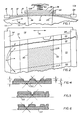
- Figs. 1 and 2 indicated generally at 10 (Fig. 1) is a portion of a magnetic-image printer, including a rotary drum 12 and an endless, belt-like conventional, magnetic imaging medium 14 carried on the drum.
- drum 12 when operating, rotates in the directon of arrow 16 at a speed of about 40-rpm.
- a read/write head array arrangement 18 including plural, side-by-side adjacent, elongated, strip-like head array structures 20, constructed in accordance with the present invention.
- structures 20 are discposed with their longitudinal axes substantially parallel to one another, and at a slight upwardly and to the right inclined angle relative to the direction (shown by arrow 16) in which medium 14 travels relatively beneath the array structures. The reason for this angular inclination will be explained shortly.
- each includes a flexible Metglas web, or substrate, shown at 22, on the top side of which in Fig. 1 (the confronting side in Fig. 2) there are formed one hundred and twenty-eight electromagnetic read/write;heads arranged in sixteen rows of eight heads each.
- the sixteen rows generally parallel the long axis of the structure, and the whole matrix of heads occupies a rhomboidal region 22a (two such regions being shaded in Fig. 2).
- the read/write axes for these heads extend substantially normal to the plane of Fig. 2, taking into account the obvious consideration that the head array structures are bent, as shown in Fig. 1 to place the undersides of webs 22 against medium 14.
- Fig. 2 Extending in Fig. 2 generally upwardly to the right and downardly to the left of the head matrix in each structure are patterns of conductors, called herein a highway system, for energizing coils in the heads. These conductors extend to terminating connection pads, the outermost of which extend substantially to the dash-double-dot lines in Fig. 2.
- each head matrix is dictated by the necessity for an angular-offset head arrangement, such as that described in my above-referred-to application, Serial No. 381,923.
- the disclosure of that application is hereby incorporated by reference into this specification.
- frame pieces 24 Suitably supporting opposite ends of webs 22 are frame pieces 24 which are mounted in the printer in any appropriate manner. These frame pieces are disposed in such a fashion that each web 22 is bent over medium 14 to place in contact with the medium an expanse on the underside of the web substantially co-extensive with that expanse on top of the web where projecting portions of the read/write heads are formed (the shaded expanses in Fig. 2). In Fig. 1, what might be thought of as the "angular" limits of these expanses, with respect to drum rotation, are depicted by dashed lines 26, 28. In Fig.
- FIG. 1 Further describing head array structures 20, formed in accordance with the teachings in my above-referenced prior U.S. patent applications, on the upper side of each web in Fig. 2, are various layers including electrical conductors and certain magnetic material which, together with the web, make up the plurality of read/write heads in the structure.
- this construction is represented schematically at 34 as a unitary lump on the top side of web 22. The actual construction and topography of this unified lump will be explained shortly.
- the lateral (right-to-left) limits of lumps 34 correspond with dashed lines 30, 32 in Fig. 2.
- a felt biasing pad 36 which is backed up, so-to-speak, by a suitable platen shown at 38.
- a biasing spring 40 which acts between the platen shown and a fragment 10a of the frame in printer 10.
- the head array structures of this invention which are thin-film floppy and compliant devices, be specially adapted for what is referred to as expanse-type, pressure-biased, substantially uniform-pressure contact with a facial zone (identified earlier) in medium 14.
- a lump 34 forming a part of what has been called a lump 34, along with the specific structural parts that cooperate with web 22 to make up read/write heads, is additional structure that tends to fill in what might be thought of as void expanses on the same side of the web so as to minimize pressure-point-telegraphing through the web to a medium under the pressure-biased operating situation depicted in Fig. 1.
- FIG. 3 here there are shown enlarged fragments of portions of two of the head array structures seen in Fig. 2.
- a description thereof is given in particular only with reference to substantially one half the length of a portion of one of the head structures, inasmuch as the other half takes the form of a reversed mirror-image replica.
- dashed circles 42, 44, 46, 48, 50, 52, 54, 56 are the perimetral outlines of eight of the electrical energizing windings provided for eight of the read/write heads in the structure now being described. Extending, as can be seen, from the left side of Fig. 3, independently toward each of these eight windings, and shown also in dashed lines, are unnumbered conductors that form what is referred to herein as a highway system to the respective windings. For reasons which will be explained shortly, one will note that various ones of these conductors, at different locations, include differently shaped lateral bulges, or expanses.
- a layer of magnetic material 58 Distributed over the windings and conductors just mentioned, ultimately as a final blanket in the head array structure, is a layer of magnetic material 58 having the perimeter outline shown, which generally repeats the pattern of windings and conductors. This material, where it overlies the windings, cooperates in the way described in the above-referred-to applications Serial Nos. 170,788 and 381,922 to form parts of the read/write heads.
- the blanket of material just described extends toward the viewer in Fig. 3, from the near plane of web 22, about the same distance all over the blanket.
- the generally circular projecting portions depicted in Fig. 3 are referred to herein as first-mentioned projecting land portions.
- the other projecting portions including those which overly the conductors, and those which characterize the islands, are referred to both as second-mentioned projecting land portions, and as point-pressure-minimizing means.
- web 22 has an overall thickness, shown at t 1 , of about 60-microns, and each of the projections above the top surface of the web in Fig. 4 has an overall thickness, shown at t 2 , of about 45-microns.
- the combined thickness, T is about 105-microns.
- FIGs. 5 and 6 taken from the other points of view mentioned, depict similar force-vector situations.
Landscapes
- Engineering & Computer Science (AREA)
- Multimedia (AREA)
- Signal Processing (AREA)
- General Engineering & Computer Science (AREA)
- Physics & Mathematics (AREA)
- General Physics & Mathematics (AREA)
- Theoretical Computer Science (AREA)
- Manufacturing & Machinery (AREA)
- Printers Or Recording Devices Using Electromagnetic And Radiation Means (AREA)
- Magnetic Heads (AREA)
- Recording Or Reproducing By Magnetic Means (AREA)
Applications Claiming Priority (2)
| Application Number | Priority Date | Filing Date | Title |
|---|---|---|---|
| US06/472,866 US4503439A (en) | 1983-03-08 | 1983-03-08 | Thin-film, compliant, non-pressure-point-telegraphing, electromagnetic read/write head structure |
| US472866 | 1983-03-08 |
Publications (1)
| Publication Number | Publication Date |
|---|---|
| EP0121975A1 true EP0121975A1 (de) | 1984-10-17 |
Family
ID=23877239
Family Applications (1)
| Application Number | Title | Priority Date | Filing Date |
|---|---|---|---|
| EP84300283A Withdrawn EP0121975A1 (de) | 1983-03-08 | 1984-01-18 | Dünnfilmaufbau für elektromagnetischen Lese/Schreibkopf |
Country Status (6)
| Country | Link |
|---|---|
| US (1) | US4503439A (de) |
| EP (1) | EP0121975A1 (de) |
| JP (1) | JPS59209155A (de) |
| FR (1) | FR2542485A1 (de) |
| GB (1) | GB2135938B (de) |
| SE (1) | SE8400079L (de) |
Cited By (3)
| Publication number | Priority date | Publication date | Assignee | Title |
|---|---|---|---|---|
| EP0176522A4 (de) * | 1984-03-15 | 1987-09-15 | Martin Mattler | Klammer/schneidinstrument und verfahren zur herstellung und entsprechende anwendung. |
| FR2603996A1 (fr) * | 1986-09-17 | 1988-03-18 | Primat Didier | Dispositif de lecture optique sans objectif |
| EP0435697A1 (de) * | 1989-12-28 | 1991-07-03 | Sharp Kabushiki Kaisha | Gerät zur magnetooptischen Aufzeichnung/Wiedergabe |
Families Citing this family (17)
| Publication number | Priority date | Publication date | Assignee | Title |
|---|---|---|---|---|
| US4739342A (en) * | 1987-04-30 | 1988-04-19 | International Business Machines Corporation | Crossed-element magnetographic print head |
| US5216559A (en) * | 1990-06-01 | 1993-06-01 | Iomega Corporation | Carrier structure for read/write heads |
| US5122917A (en) * | 1990-06-01 | 1992-06-16 | Iomega Corporation | Unitary read-write head array for magnetic media |
| US5544774A (en) * | 1994-08-26 | 1996-08-13 | Aiwa Research And Development, Inc. | Method of eliminating pole recession in a thin film magnetic head |
| US5563754A (en) * | 1994-08-26 | 1996-10-08 | Aiwa Research And Development, Inc. | Thin film magnetic head including a durable wear layer and gap structure |
| US5801909A (en) * | 1994-08-26 | 1998-09-01 | Aiwa Research And Development, Inc. | Thin film magnetic head including durable wear layer and non-magnetic gap structures |
| US5748417A (en) * | 1994-08-26 | 1998-05-05 | Aiwa Research And Development, Inc. | Thin film magnetic head including layered magnetic side poles |
| US5754377A (en) * | 1994-08-26 | 1998-05-19 | Aiwa Research And Development, Inc. | Thin film magnetic head including an elevated gap structure |
| US5909346A (en) * | 1994-08-26 | 1999-06-01 | Aiwa Research & Development, Inc. | Thin magnetic film including multiple geometry gap structures on a common substrate |
| US5673474A (en) * | 1994-08-26 | 1997-10-07 | Aiwa Research And Development, Inc. | Method of fabricating a thin film magnetic head including layered magnetic side poles |
| US6091581A (en) * | 1994-08-26 | 2000-07-18 | Aiwa Co., Ltd. | Thin film magnetic head including a separately deposited diamond-like carbon gap structure and magnetic control wells |
| JPH08171712A (ja) * | 1994-08-26 | 1996-07-02 | Aiwa Co Ltd | 側面露出型薄膜磁気ヘッド並びにその製造方法 |
| US5490028A (en) * | 1994-08-26 | 1996-02-06 | Aiwa Research And Development, Inc. | Thin film magnetic head including an integral layered shield structure |
| US5621594A (en) * | 1995-02-17 | 1997-04-15 | Aiwa Research And Development, Inc. | Electroplated thin film conductor coil assembly |
| US6069015A (en) * | 1996-05-20 | 2000-05-30 | Aiwa Research And Development, Inc. | Method of fabricating thin film magnetic head including durable wear layer and non-magnetic gap structure |
| JP3963637B2 (ja) * | 2000-09-04 | 2007-08-22 | 富士フイルム株式会社 | 磁気転写方法 |
| JP2002074656A (ja) * | 2000-09-04 | 2002-03-15 | Fuji Photo Film Co Ltd | 磁気転写方法 |
Citations (5)
| Publication number | Priority date | Publication date | Assignee | Title |
|---|---|---|---|---|
| US2820956A (en) * | 1956-04-03 | 1958-01-21 | Ibm | Magnetic printing machine |
| DE2423836A1 (de) * | 1973-05-24 | 1974-12-19 | Honeywell Inc | Magnetaufzeichnungskopf |
| DE3007046A1 (de) * | 1979-02-28 | 1980-09-11 | Philips Nv | Mehrspuren-duennfilmmagnetkopf |
| DE3048773A1 (de) * | 1979-12-26 | 1981-09-24 | Ampex Corp., 94063 Redwood City, Calif. | Magnetwandleraufbau mit mehreren stegen |
| US4414554A (en) * | 1980-07-21 | 1983-11-08 | Ferix Corporation | Magnetic imaging apparatus |
-
1983
- 1983-03-08 US US06/472,866 patent/US4503439A/en not_active Expired - Fee Related
-
1984
- 1984-01-09 GB GB08400414A patent/GB2135938B/en not_active Expired
- 1984-01-10 SE SE8400079A patent/SE8400079L/ not_active Application Discontinuation
- 1984-01-18 EP EP84300283A patent/EP0121975A1/de not_active Withdrawn
- 1984-01-27 JP JP59013233A patent/JPS59209155A/ja active Pending
- 1984-03-06 FR FR8403452A patent/FR2542485A1/fr not_active Withdrawn
Patent Citations (5)
| Publication number | Priority date | Publication date | Assignee | Title |
|---|---|---|---|---|
| US2820956A (en) * | 1956-04-03 | 1958-01-21 | Ibm | Magnetic printing machine |
| DE2423836A1 (de) * | 1973-05-24 | 1974-12-19 | Honeywell Inc | Magnetaufzeichnungskopf |
| DE3007046A1 (de) * | 1979-02-28 | 1980-09-11 | Philips Nv | Mehrspuren-duennfilmmagnetkopf |
| DE3048773A1 (de) * | 1979-12-26 | 1981-09-24 | Ampex Corp., 94063 Redwood City, Calif. | Magnetwandleraufbau mit mehreren stegen |
| US4414554A (en) * | 1980-07-21 | 1983-11-08 | Ferix Corporation | Magnetic imaging apparatus |
Cited By (5)
| Publication number | Priority date | Publication date | Assignee | Title |
|---|---|---|---|---|
| EP0176522A4 (de) * | 1984-03-15 | 1987-09-15 | Martin Mattler | Klammer/schneidinstrument und verfahren zur herstellung und entsprechende anwendung. |
| FR2603996A1 (fr) * | 1986-09-17 | 1988-03-18 | Primat Didier | Dispositif de lecture optique sans objectif |
| EP0261027A1 (de) * | 1986-09-17 | 1988-03-23 | Up Systems | Optische Lesevorrichtung ohne Objektiv |
| EP0435697A1 (de) * | 1989-12-28 | 1991-07-03 | Sharp Kabushiki Kaisha | Gerät zur magnetooptischen Aufzeichnung/Wiedergabe |
| US5068841A (en) * | 1989-12-28 | 1991-11-26 | Sharp Kabushiki Kaisha | Magneto-optical recording/reproducing device |
Also Published As
| Publication number | Publication date |
|---|---|
| FR2542485A1 (fr) | 1984-09-14 |
| JPS59209155A (ja) | 1984-11-27 |
| SE8400079L (sv) | 1984-09-09 |
| US4503439A (en) | 1985-03-05 |
| GB2135938A (en) | 1984-09-12 |
| GB8400414D0 (en) | 1984-02-08 |
| GB2135938B (en) | 1986-01-15 |
| SE8400079D0 (sv) | 1984-01-10 |
Similar Documents
| Publication | Publication Date | Title |
|---|---|---|
| US4503439A (en) | Thin-film, compliant, non-pressure-point-telegraphing, electromagnetic read/write head structure | |
| KR100214163B1 (ko) | 반도체 공정용 개량된 복합 폴리싱 패드 | |
| DE69830944T2 (de) | Polierkissen mit Rillenmuster zur Verwendung in einer chemisch-mechanischen Poliervorrichtung | |
| US6273806B1 (en) | Polishing pad having a grooved pattern for use in a chemical mechanical polishing apparatus | |
| US6634936B2 (en) | Chemical mechanical planarization or polishing pad with sections having varied groove patterns | |
| US5609517A (en) | Composite polishing pad | |
| MY112281A (en) | Improved polishing pads and methods for their use | |
| US5604021A (en) | Multi-layer support pad having regions of differing firmness | |
| GB2361801B (en) | Read head with read track width defining layer that planarizes the write gap layer of a write head | |
| RU98112762A (ru) | Машина для тиснения и ламинирования с цилиндрами с рассредоточенными участками контакта и способ тиснения и ламинирования | |
| KR100388929B1 (ko) | 압전식 구동 cmp 캐리어를 구비하는 장치 및 그 구동방법 | |
| KR980000766A (ko) | 연마패드 및 그를 갖는 연마장치 | |
| NO20053603L (no) | Syntetisk gressoverflate. | |
| RU98112268A (ru) | Машина для тиснения и ламинирования, тисненое листовое изделие и способ тиснения полосового материала | |
| AP1594A (en) | Synthetic grass with resilient granular top surface layer. | |
| EP0844561A3 (de) | Speicherplattenanordnung und Steuerungsverfahren dafür | |
| EP1002651A3 (de) | Seriendrucker und Verfahren zur Einstellung der Bogenvorschublänge | |
| AU2003293596A1 (en) | Drive belt with transverse elements and stamping device for producing transverse elements | |
| ATE55161T1 (de) | Teppichfliese mit antistatischen eigenschaften und deren vorbereitungsverfahren. | |
| CA2258200C (en) | Flexible abrasive member having interlocking deposits | |
| US5873772A (en) | Method for polishing the top and bottom of a semiconductor wafer simultaneously | |
| KR970077301A (ko) | 기판 폴리싱 장치 | |
| JPH086096Y2 (ja) | 護床工ブロック | |
| JPH1148131A (ja) | 基板を平坦化するための研磨工具および研磨方法 | |
| JPH08150557A (ja) | 研磨パッド |
Legal Events
| Date | Code | Title | Description |
|---|---|---|---|
| PUAI | Public reference made under article 153(3) epc to a published international application that has entered the european phase |
Free format text: ORIGINAL CODE: 0009012 |
|
| AK | Designated contracting states |
Designated state(s): BE CH DE IT LI NL |
|
| 17P | Request for examination filed |
Effective date: 19841029 |
|
| STAA | Information on the status of an ep patent application or granted ep patent |
Free format text: STATUS: THE APPLICATION IS DEEMED TO BE WITHDRAWN |
|
| 18D | Application deemed to be withdrawn |
Effective date: 19860211 |
|
| RIN1 | Information on inventor provided before grant (corrected) |
Inventor name: SPRINGER, GILBERT DUANE |