EP0122119A2 - Leseverstärker - Google Patents
Leseverstärker Download PDFInfo
- Publication number
- EP0122119A2 EP0122119A2 EP84302328A EP84302328A EP0122119A2 EP 0122119 A2 EP0122119 A2 EP 0122119A2 EP 84302328 A EP84302328 A EP 84302328A EP 84302328 A EP84302328 A EP 84302328A EP 0122119 A2 EP0122119 A2 EP 0122119A2
- Authority
- EP
- European Patent Office
- Prior art keywords
- transistor
- output
- sense amplifier
- transistors
- pair
- Prior art date
- Legal status (The legal status is an assumption and is not a legal conclusion. Google has not performed a legal analysis and makes no representation as to the accuracy of the status listed.)
- Granted
Links
Images


Classifications
-
- G—PHYSICS
- G11—INFORMATION STORAGE
- G11C—STATIC STORES
- G11C7/00—Arrangements for writing information into, or reading information out from, a digital store
- G11C7/06—Sense amplifiers; Associated circuits, e.g. timing or triggering circuits
- G11C7/062—Differential amplifiers of non-latching type, e.g. comparators, long-tailed pairs
Definitions
- the present invention relates to a sense amplifier, and more particularly to a complementary metal-oxide semiconductor (CMOS) high-speed sense amplifier for amplifying a potential difference between a pair of bit lines or a pair of data buses in a static semiconductor memory.
- CMOS complementary metal-oxide semiconductor
- each transistor constituting a memory cell has become more and more miniaturized.
- This miniaturization has reduced the driving capability of a transistor, lowered the speed of the potential change, during reading, of a pair of bit lines or a pair of data buses connected to a sense amplifier, and decreased the potential difference between a pair of bit lines or a pair of data buses.
- an improved high-speed sense amplifier is necessary.
- a conventional sense amplifier cannot provide high-speed operation with such a decreased and slow changing potential difference, because of the long rising period and large amplitude of the output signal, as described later in more detail.
- An embodiment of the present invention can provide a sense amplifier which can operate at high speed in response to a change of potential of a pair of bit lines or a pair of data lines.
- An embodiment of the present invention can also provide a sense amplifier which can change the output potential at a high speed in response to a change of potential of a pair of bit lines or a pair of data lines.
- a sense amplifier employs two asymmetrical differential amplifiers connected to each other in such a way that their outputs are accelerated, to charge up one another by utilizing nodes at which potentials are changed in response to a change of the input signal supplied from a pair of bit lines or a pair of data lines.
- a sense amplifier comprising a pair of differential amplifier circuits each including a pair of differential input transistors for receiving complementary signals and a feedback transistor connected to a commonly connecting point of the pair of differential input transistors and having a control input connected to an output of one of the differential input transistors.
- the complementary signals applied to one of the pair of differential amplifier circuits have phases opposite to the phases of the complementary signals applied to the other of the pair of differential amplifier circuits.
- At least one of the pair of differential amplifier circuits has a first output pull up transistor and a second output pull up transistor connected in parallel between a power supply line and an output end.
- the first output pull up transistor has a control input connected to the control input of the feedback transistor.
- the second output pull up transistor has a control input connected to an output of the feedback transistor in the other of the differential amplifier circuits.
- the conventional sense amplifier consists of two asymmetrical differential amplifiers D 01 and D 02 .
- the first differential amplifier D 01 includes N-channel input transistors Q 01 and Q 02 , P-channel pull-up transistors Q 03 and Q 04 , and an N-channel feedback transistor Q 05 .
- a pair of bit lines BL and BL are connected to the gates of the input transistors Q 01 and Q 02 , respectively.
- An output signal DA is obtained at a commonly connecting point between the drain of the P-channel pull-up transistor Q 03 and the drain of the N-channel input transistor Q 02 .
- the second differential amplifier D 02 has the same constitution as the first sense amplifier unit D O1 and includes transistors Q 01' through Q 05 '.
- the transistor Q 01 When the bit line BL is at a high potential (H) and the bit line BL is at a low potential (L), in the first differential amplifier D 01 , the transistor Q 01 has a high mutual conductance (g m (H)) and the transistor Q 02 has a low mutual conductance g m (L). Therefore, the P-channel pull up transistors Q 04 and Q 05 receive a low potential at their gates and have high mutual conductance g (H). Thus, the output signal DA is at a high level.
- the feedback transistor Q 05 receives a low potential at its gate and has low mutual conductance g m (L), ensuring the high level of the output signal DA.
- the transistors Q 01 ', Q 03 ', and Q 04 ' have the low mutual conductance g m (L), and the transistors Q 02 1 and Q 05 ' have the high mutual conductance g m (H), so that the output signal DA is at a low level.
- the conventional sense amplifier shown in Fig. 1 has a disadvantage of low-speed operation. That is, it takes a considerably long period from a time at which a pair of bit lines inverts its potential to a time at which a pair of the output potentials of the sense amplifier are inverted. This is because the output potential is raised only by the single pull-up transistor Q 03 or Q 03 ', and the output potential is lowered only by the single transistor Q02 or Q 02 '.
- Another reason for low-speed operation is that the amplitude of the output signal DA or DA, which is determined by the transistors Q 03 ' Q 02 , and Q 05 , is relatively large.
- Figure 2 shows part of a semiconductor memory device to which the present invention may be applied.
- Fig. 3 is a waveform diagram showing the operation of the device shown in Fig. 2.
- clock signals ⁇ 1 and ⁇ 2 are applied to the gates of precharging transistors Q 3 and Q 10 , bit lines BL and BL, and data lines DL and DL are shortcircuited.
- the bit lines BL and BL are precharged through transistors Q 1 and Q 2 to have a high potential.
- a word line for example, word line WD 1 is selected to have high potential
- one of the bit lines BL and BL for example, BL, is turned to a low potential, depending on the contents of a selected memory cell.
- bit-line selecting signal BS is applied to the gates of transfer-gate transistors Q 8 and Q 9 .
- the potentials of the bit lines BL and BL are transferred through the transistors Q 8 and Q 9 to the data lines DL and DL.
- a sense amplifier SA amplifies the potential difference between the data lines DL and DL. According to the present invention, the sense amplifier SA is improved, as later described in detail.
- Another example of a semiconductor memory device is known in which a pair of bit lines are precharged to have an intermediate potential between a high potential and a low potential.
- the present invention is effective whether a pair of bit lines are precharged to have a high potential or to have an intermediate potential.
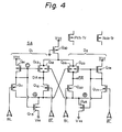
- FIG. 4 is a circuit diagram showing a sense amplifier according to an embodiment of the present invention.
- a sense amplifier SA consists of a first differential amplifier D1 and a second differential amplifier D2.
- the first differential amplifier D 1 comprises a first input transistor Q 11 , a second input transistor Q 12 , a first output pull up transistor Q 13 ' a pull up transistor Q 14 , a feedback transistor Q 15 , and a second output pull up transistor Q1 6 .
- the transistors Q 13 , Q 14 , and Q 16 are P channel metal-oxide semiconductor (MOS) transistors, and the transistors Q 11 , Q 12 , and Q 15 are N channel MOS transistors.
- a bit line BL is connected to the gate of the first input transistor Q 11 .
- MOS metal-oxide semiconductor
- a bit line BL is connected to the gate of the second input transistor Q 12 .
- the drain of the first input transistor Q 11 is connected to the gate and the drain of the pull up transistor Q14 , to the gate of the first output pull up transistor Q 13 , and to the gate of the feedback transistor Q 15 .
- the source of the pull up transistor Q 14 is connected to a power supply V CC .
- the drains of the first and the second output pull up transistors Q 13 and Q 16 are connected to the drain of the second input transistor Q 12 .
- the sources of the first and the second input transistors Q 11 and Q 12 are connected to the drain of the feedback transistor Q 15 .
- the source of the feedback transistor Q 15 is connected to a ground line V SS .
- An output end DA is connected to a point between the drains of the output pull up transistor Q 13 or Q 16 and the second input transistor Q 12'
- the second output pull up transistor Q 16 is provided according to the present invention.
- the circuit constitution of the second differential amplifier D 2 may similar to that of the first differential amplifier D 1 , and includes a first input transistor Q 21 , a second input transistor Q22 , a first output pull up transistor Q 23 , a pull up transistor Q 24 , a feedback transistor Q25 , and a second output pull up transistor Q 26 . It should be noted, however, that, in contrast to the first differential amplifier D 1 , the second differential amplifier D 2 receives a signal on the bit line BL at the gate of the second input transistor Q 22 and receives a signal on the bit line BL at the gate of the first input transistor Q 21 .
- the signals on the bit lines BL and BL, after the bit lines are selected, are complementary.
- the above- mentioned contrast lies in the fact that the complementary signals applied to the first differential amplifier D 1 have opposite phases to the complementary signals applied to the second differential amplifier D 2 .
- an output amplitude determining transistor Q 20 is provided between the sources of the output pull up transistors Q 13 , Q 16 ' Q 23 ' and Q 26 and the power supply V CC .
- the transistor Q 20 in this embodiment is a P-channel MOS transistor.
- the source of the transistor Q 20 is connected to the power supply V CC .
- the drain of the transistor Q 20 is connected to the sources of the transistors Q 13 ' Q 16 ' Q 23 , and Q 26 .
- the gate of the transistor Q 20 is grounded. Accordingly, the transistor Q 20 is normally in a conductive state.
- the sources of the input transistors Q 11 and Q 12 in the first differential amplifier D 1 are connected to the gate of the second output pull up transistor Q 26 in the second differential amplifier D 2 .
- the sources of the input transistors Q 21 and Q 22 are connected to the gate of the second pull up transistor Q 16 in the first differential amplifier D 1 .
- the first differential amplifier D 1 and the second differential amplifier D 2 each constitute a complementary MOS (CMOS) differential amplifier having P channel output pull up transistor and N channel input transistor
- CMOS complementary MOS
- the second output pull up transistors Q 16 and Q 26 function to accelerate the charging up of the output ends DA and DA, respectively.
- the conventional sense amplifier shown in Fig. 1 is equivalent to the circuit in which the second output pull up transistors Q 16 and Q 26 and the output amplitude determining transistor Q 20 are removed from the circuit shown in Fig. 4.
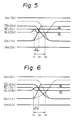
- Figure 5 is a waveform diagram showing an example of the operation of the circuit shown in Fig. 4.
- the potential of the power supply V CC is assumed to be about 5 V
- the potential of the ground line V SS is assumed to be about 0 V.
- the bit line BL is at the low potential (L level) of about 2.5 V
- the bit line BL is at the high potential (H level) of about 3 V. Because of the miniaturization of memory cells as mentioned before, the potential difference between bit lines may be as small as 0.5 V.
- the first input transistor Q 11 has a low mutual conductance g m (L), so that the potential at a node C connected to the gates of the transistors Q 13 and Q 14 is at a high level, causing the P-channel transistors Q 13 and Q 14 to have a low mutual conductance g m (L), and causing the N-channel feedback transistor Q 15 to have a high mutual conductance g m (H). Also, because the H level is applied to the gate of the second input transistor Q 12 , it has a high mutual conductance g m (H).
- the first input transistor Q 21 has the high mutual conductance g m (H) and, accordingly, the P-channel transistors Q 23 and Q 24 have the high mutual conductance g m (H).
- the feedback transistor Q 25 has the low mutual conductance g m (L).
- the second input transistor Q 22 has the low mutual conductance g m (L).
- the feedback transistor Q 25 Since the feedback transistor Q 25 has the low mutual conductance g m (L), the potential at a node B connected to the drain of transistor Q 25 is at a high level. The node is connected to the gate of the second output pull up transistor Q 16 in the first differential amplifier D 1 . Therefore transistor Q 16 has the low mutual conductance g m (L). As a result, in the first differential amplifier D 1 , transistors Q 13 and Q 16 have the low mutual conductance g m (L), and transistors Q 12 and Q 15 have the high mutual conductance g m (H), so that the potential at the output end DA is at a low level of about 1 V.
- the feedback transistor Q 15 Since the feedback transistor Q 15 has the high mutual conductance g m (H), the potential at a node 0 connected to the drain of the transistor Q15 is at a low level.
- the node A is connected to the gate of the second output pull up transistor Q 26 in the second differential amplifier D 2 . Therefore, transistor Q 26 has the high mutual conductance g m (H).
- the transistors Q23 and Q 26 have the high mutual conductance g m (H)
- the transistors Q 22 and Q 25 have the low mutual conductance g m (L), so that the potential at the output end DA is at a high level of about 3.5 V.
- the pair of bit lines BL and BL are precharged to the same potential of 3 V.
- the transistors Q 11 , Q 13 and Q 14 in the first differential amplifier D 1 , and the transistor Q 22 in the second differential amplifier D 2 change to having high mutual conductance g m (H).
- the transistor Q 15 changes to low mutual conductance g m (L).
- the potentials of the bit lines BL and BL are inverted in accordance with the content of the selected memory cell, so that the bit line BL is kept at the high potential of 3 V and the bit line BL is turned to the low potential of 2.5 V. Since the feedback transistor Q 15 has, at this stage, the low mutual conductance g m (L), the potential at the node 0 is raised so that the mutual conductance of the transistor Q 26 is lowered. On the other hand, in the second differential amplifier D 2 , transistors Q 21 , Q 23 , and Q 24 have, at this stage, the low mutual conductance g m (L), and the transistors Q 22 and Q 25 have the high mutual conductance g m (H).
- the potential at the node B is lowered so that the mutual conductance of the transistor Q 16 for accelerating the charging of the output end DA is increased.
- the potential at node B is lower than the potential at node which is also at a low level. Therefore, the second output pull up transistor Q 16 becomes more active than the first output pull up transistor Q 13 . As a result, the second output pull up transistor Q 16 is rapidly turned more conductive, accelerating the charge up of the output end DA to the high level of about 3.5 V.
- the transistors Q 23 and Q 26 are turned to have the low mutual conductance g m (L) and the transistors Q 22 and Q 25 are turned to have the high mutual conductance g m (H), so that the charges stored at the output end DA are discharged through the transistors Q 22 and Q 25 to the ground line V SS .
- the potential at the output end DA gradually decreases, and as a result, at a time t 2 , the potentials at the output ends DA and DA are inverted.
- a period At between the time t 1 and the time t 2 is a response period of the sense amplifier SA in response to an inversion of the bit lines.
- the response period At is shortened in comparison with the conventional response period.
- One reason for this is because the rise of the potential at the output end DA is accelerated by the function of the second output pull up transistor Q 16 .
- Another reason is that the high level of potential at the output end DA is limited to a relatively low voltage of about 3.5 V by providing the output amplitude determining transistor Q20.
- the high level of potential at the output end DA is adjustable by varying the dimensions of the transistors Q 16 and Q 20 .
- the operation of the sense amplifier SA in response to a potential change of the bit line BL from the high level to the low level is similar to the operation described above.
- the potential at the output end DA rises in response to the increase of the mutual conductance of the transistor Q 03 and to the decrease of the mutual conductance of the transistor Q 02 .
- the rise of the potential at the output end DA is very slow and the high level is higher in comparison with the embodiment of the present invention.
- a time t 3 at which the potentials of the output ends DA and DA of the dash curves cross, is later than the time t 2 in the embodiment of the present invention.
- the transistors Q 01 , Q 02 , Q 03 , and Q 04 have high mutual conductance g m (H), and the transistor Q 05 has low mutual conductance g m (L).
- the transistor Q 02 changes to low mutual conductance g m (L).
- the potential at the output end DA is pulled up through the transistor Q 03 . Therefore, only the second input transistor Q02 changes its state to assist the rise of the potential at the output end DA. No acceleration to raise the output potential is carried out in the conventional sense amplifier.
- Figure 6 is a waveform diagram showing another example of the operation of the circuit shown in Fig. 4.
- the only difference from Fig. 5 is that the pair of bit lines BL and BL are precharged not to the high level of about 3 V but to an intermediate level between 3 V and 2.5 V.
- the operation of the sense amplifier SA in this case is similar to that described with reference to Fig. 5, and therefore, is not described here.
- CMOS complementary metal-oxide-semiconductor
- CMOS complementary metal-oxide-semiconductor
- any other type of asymmetrical differential amplifier may be employed within the scope of the present invention.
- a sense amplifier according to the present invention, by employing two asymmetrical differential amplifiers which may have the same circuit configuration, and by connecting them so as to accelerate charging up of the outputs of the asymmetrical differential amplifiers by utilizing nodes whose potentials are changed in response to changes of input potentials, a sense amplifier according to the present invention can change its output potential at a higher speed than the conventional sense amplifier.
Landscapes
- Static Random-Access Memory (AREA)
- Dram (AREA)
Applications Claiming Priority (2)
| Application Number | Priority Date | Filing Date | Title |
|---|---|---|---|
| JP60032/83 | 1983-04-07 | ||
| JP58060032A JPS59186188A (ja) | 1983-04-07 | 1983-04-07 | センス増幅器 |
Publications (3)
| Publication Number | Publication Date |
|---|---|
| EP0122119A2 true EP0122119A2 (de) | 1984-10-17 |
| EP0122119A3 EP0122119A3 (en) | 1987-10-28 |
| EP0122119B1 EP0122119B1 (de) | 1990-02-28 |
Family
ID=13130319
Family Applications (1)
| Application Number | Title | Priority Date | Filing Date |
|---|---|---|---|
| EP84302328A Expired EP0122119B1 (de) | 1983-04-07 | 1984-04-05 | Leseverstärker |
Country Status (4)
| Country | Link |
|---|---|
| US (1) | US4606012A (de) |
| EP (1) | EP0122119B1 (de) |
| JP (1) | JPS59186188A (de) |
| DE (1) | DE3481462D1 (de) |
Cited By (1)
| Publication number | Priority date | Publication date | Assignee | Title |
|---|---|---|---|---|
| EP0297715A3 (de) * | 1987-05-29 | 1989-10-25 | AT&T Corp. | Differenzverstärkereingangsstufe für Leitungsempfänger und für Operationsverstärker |
Families Citing this family (8)
| Publication number | Priority date | Publication date | Assignee | Title |
|---|---|---|---|---|
| JPH0618308B2 (ja) * | 1985-04-08 | 1994-03-09 | ソニー株式会社 | 平衡型差動増幅器 |
| US4713797A (en) * | 1985-11-25 | 1987-12-15 | Motorola Inc. | Current mirror sense amplifier for a non-volatile memory |
| JP2514330B2 (ja) * | 1986-05-30 | 1996-07-10 | 日本テキサス・インスツルメンツ株式会社 | センスアンプ回路 |
| FR2603414B1 (fr) * | 1986-08-29 | 1988-10-28 | Bull Sa | Amplificateur de lecture |
| JPH0727717B2 (ja) * | 1988-07-13 | 1995-03-29 | 株式会社東芝 | センス回路 |
| JP2672721B2 (ja) * | 1991-05-27 | 1997-11-05 | 株式会社東芝 | センスアンプ回路 |
| US6407590B2 (en) * | 2000-03-07 | 2002-06-18 | Texas Instruments Incorporated | High frequency differential receiver |
| JP4707099B2 (ja) * | 2005-08-23 | 2011-06-22 | ルネサスエレクトロニクス株式会社 | 差動出力回路 |
Family Cites Families (3)
| Publication number | Priority date | Publication date | Assignee | Title |
|---|---|---|---|---|
| US3983412A (en) * | 1975-07-02 | 1976-09-28 | Fairchild Camera And Instrument Corporation | Differential sense amplifier |
| JPS5824874B2 (ja) * | 1979-02-07 | 1983-05-24 | 富士通株式会社 | センス回路 |
| JPS57198594A (en) * | 1981-06-01 | 1982-12-06 | Hitachi Ltd | Semiconductor storage device |
-
1983
- 1983-04-07 JP JP58060032A patent/JPS59186188A/ja active Granted
-
1984
- 1984-04-04 US US06/596,707 patent/US4606012A/en not_active Expired - Lifetime
- 1984-04-05 DE DE8484302328T patent/DE3481462D1/de not_active Expired - Lifetime
- 1984-04-05 EP EP84302328A patent/EP0122119B1/de not_active Expired
Cited By (1)
| Publication number | Priority date | Publication date | Assignee | Title |
|---|---|---|---|---|
| EP0297715A3 (de) * | 1987-05-29 | 1989-10-25 | AT&T Corp. | Differenzverstärkereingangsstufe für Leitungsempfänger und für Operationsverstärker |
Also Published As
| Publication number | Publication date |
|---|---|
| JPS59186188A (ja) | 1984-10-22 |
| DE3481462D1 (de) | 1990-04-05 |
| EP0122119B1 (de) | 1990-02-28 |
| EP0122119A3 (en) | 1987-10-28 |
| JPH0241114B2 (de) | 1990-09-14 |
| US4606012A (en) | 1986-08-12 |
Similar Documents
| Publication | Publication Date | Title |
|---|---|---|
| US4417328A (en) | Random access semiconductor memory device using MOS transistors | |
| EP0015070B1 (de) | Leseverstärkerschaltung | |
| US5638332A (en) | Integrated circuit memory device with balancing circuit including follower amplifier coupled to bit line | |
| EP0398245B1 (de) | Direktzugriffsspeicher vom dynamischen Typ | |
| US5844845A (en) | Data read circuit for use in semiconductor storage apparatus of CMOS memory | |
| JPH0713857B2 (ja) | 半導体記憶装置 | |
| US4370737A (en) | Sense amplifier and sensing methods | |
| JPH0422318B2 (de) | ||
| KR19990072294A (ko) | 감지증폭기장치및디지탈데이타출력신호발생방법 | |
| JP2862744B2 (ja) | 半導体メモリ装置のデータ出力バッファ | |
| JPH06132747A (ja) | 半導体装置 | |
| US5148399A (en) | Sense amplifier circuitry selectively separable from bit lines for dynamic random access memory | |
| EP0122119B1 (de) | Leseverstärker | |
| KR900008917B1 (ko) | 반도체 메모리 소자의 데이타 판독회로 | |
| KR100203717B1 (ko) | 반도체 기억장치의 데이터버스 클램프회로 | |
| US4860257A (en) | Level shifter for an input/output bus in a CMOS dynamic ram | |
| US5305272A (en) | Sense amplifier circuit | |
| JPH04238197A (ja) | センスアンプ回路 | |
| US4858193A (en) | Preamplification method and apparatus for dram sense amplifiers | |
| US4467456A (en) | Memory circuit | |
| KR910004733B1 (ko) | 데이타 버스 리셋트 회로를 지닌 반도체 기억장치 | |
| US5018105A (en) | Semiconductor memory device | |
| KR940004516B1 (ko) | 반도체 메모리의 고속 센싱장치 | |
| JP2680939B2 (ja) | 半導体記憶装置 | |
| JP2523736B2 (ja) | 半導体記憶装置 |
Legal Events
| Date | Code | Title | Description |
|---|---|---|---|
| PUAI | Public reference made under article 153(3) epc to a published international application that has entered the european phase |
Free format text: ORIGINAL CODE: 0009012 |
|
| AK | Designated contracting states |
Designated state(s): DE FR GB |
|
| PUAL | Search report despatched |
Free format text: ORIGINAL CODE: 0009013 |
|
| AK | Designated contracting states |
Kind code of ref document: A3 Designated state(s): DE FR GB |
|
| 17P | Request for examination filed |
Effective date: 19871216 |
|
| 17Q | First examination report despatched |
Effective date: 19890410 |
|
| GRAA | (expected) grant |
Free format text: ORIGINAL CODE: 0009210 |
|
| AK | Designated contracting states |
Kind code of ref document: B1 Designated state(s): DE FR GB |
|
| ET | Fr: translation filed | ||
| REF | Corresponds to: |
Ref document number: 3481462 Country of ref document: DE Date of ref document: 19900405 |
|
| PLBE | No opposition filed within time limit |
Free format text: ORIGINAL CODE: 0009261 |
|
| STAA | Information on the status of an ep patent application or granted ep patent |
Free format text: STATUS: NO OPPOSITION FILED WITHIN TIME LIMIT |
|
| 26N | No opposition filed | ||
| REG | Reference to a national code |
Ref country code: GB Ref legal event code: IF02 |
|
| PGFP | Annual fee paid to national office [announced via postgrant information from national office to epo] |
Ref country code: GB Payment date: 20030402 Year of fee payment: 20 |
|
| PGFP | Annual fee paid to national office [announced via postgrant information from national office to epo] |
Ref country code: FR Payment date: 20030408 Year of fee payment: 20 |
|
| PGFP | Annual fee paid to national office [announced via postgrant information from national office to epo] |
Ref country code: DE Payment date: 20030417 Year of fee payment: 20 |
|
| PG25 | Lapsed in a contracting state [announced via postgrant information from national office to epo] |
Ref country code: GB Free format text: LAPSE BECAUSE OF EXPIRATION OF PROTECTION Effective date: 20040404 |
|
| REG | Reference to a national code |
Ref country code: GB Ref legal event code: PE20 |