EP0122632A2 - Schaltungsanordnung zur Demodulation eines FM-Signales - Google Patents
Schaltungsanordnung zur Demodulation eines FM-Signales Download PDFInfo
- Publication number
- EP0122632A2 EP0122632A2 EP84104334A EP84104334A EP0122632A2 EP 0122632 A2 EP0122632 A2 EP 0122632A2 EP 84104334 A EP84104334 A EP 84104334A EP 84104334 A EP84104334 A EP 84104334A EP 0122632 A2 EP0122632 A2 EP 0122632A2
- Authority
- EP
- European Patent Office
- Prior art keywords
- signal
- transistor
- inverters
- inverter
- demodulation circuit
- Prior art date
- Legal status (The legal status is an assumption and is not a legal conclusion. Google has not performed a legal analysis and makes no representation as to the accuracy of the status listed.)
- Withdrawn
Links
- 239000003990 capacitor Substances 0.000 claims abstract description 26
- 238000002347 injection Methods 0.000 claims abstract description 8
- 239000007924 injection Substances 0.000 claims abstract description 8
- 238000010586 diagram Methods 0.000 description 8
- 230000009467 reduction Effects 0.000 description 4
- 238000010276 construction Methods 0.000 description 3
- 230000003071 parasitic effect Effects 0.000 description 3
- 230000004044 response Effects 0.000 description 3
- 239000000758 substrate Substances 0.000 description 2
- 230000007547 defect Effects 0.000 description 1
- 230000003111 delayed effect Effects 0.000 description 1
- 230000001419 dependent effect Effects 0.000 description 1
- 230000001788 irregular Effects 0.000 description 1
- 238000004519 manufacturing process Methods 0.000 description 1
- 239000002184 metal Substances 0.000 description 1
- 230000004048 modification Effects 0.000 description 1
- 238000012986 modification Methods 0.000 description 1
- 230000002265 prevention Effects 0.000 description 1
- 229920006395 saturated elastomer Polymers 0.000 description 1
- 230000036962 time dependent Effects 0.000 description 1
Images


Classifications
-
- H—ELECTRICITY
- H03—ELECTRONIC CIRCUITRY
- H03D—DEMODULATION OR TRANSFERENCE OF MODULATION FROM ONE CARRIER TO ANOTHER
- H03D3/00—Demodulation of angle-, frequency- or phase- modulated oscillations
-
- H—ELECTRICITY
- H03—ELECTRONIC CIRCUITRY
- H03D—DEMODULATION OR TRANSFERENCE OF MODULATION FROM ONE CARRIER TO ANOTHER
- H03D3/00—Demodulation of angle-, frequency- or phase- modulated oscillations
- H03D3/02—Demodulation of angle-, frequency- or phase- modulated oscillations by detecting phase difference between two signals obtained from input signal
- H03D3/04—Demodulation of angle-, frequency- or phase- modulated oscillations by detecting phase difference between two signals obtained from input signal by counting or integrating cycles of oscillations
-
- H—ELECTRICITY
- H03—ELECTRONIC CIRCUITRY
- H03D—DEMODULATION OR TRANSFERENCE OF MODULATION FROM ONE CARRIER TO ANOTHER
- H03D2200/00—Indexing scheme relating to details of demodulation or transference of modulation from one carrier to another covered by H03D
- H03D2200/0041—Functional aspects of demodulators
- H03D2200/0084—Lowering the supply voltage and saving power
Definitions
- This invention relates to an FM signal demodulation circuit suitable for use in a reproduction circuit of a video tape recorder or the like.
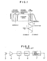
- a carrier which defines a sync tip (tip of the synchronizing signal) 1 at 3.4 MHz and a white peak (peak white level of the video signal) 2 at 4.4 MHz so as to occupy a band of about 1 MHz, as shown in F ig. 1.
- Fig. 2 illustrates, in block form, a reproduction circuit used in this type of video tape recorder.
- a signal reproduced by a head 3 is amplified by a pre-amplifier 4 and then regenerated and equalized by means of an equalizer 5.
- a resulting signal is demodulated by a demodulation circuit 6 and passed through a video signal processing circuit 7 to provide a video signal v.
- the demodulation circuit 6. is of a pulse count type.
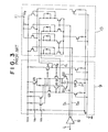
- Fig. 3 illustrates a prior art pulse count type demodulation circuit
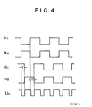
- Fig. 4 illustrates signal waveforms appearing at the essential parts of the Fig. 3 circuit.
- An input signal i is inputted to a limiter 8, which in turn delivers wave-shaped output signals b 1 and b 2 which are out of phase from each other by 180°.
- These output signals b 1 and b 2 are respectively applied to bases of transistors Q 1 and Q 2 included in a delay circuit 9, so that signals a 1 and q 2 are produced from emitters of transistors Q 3 and Q4, respectively, these signals a 1 and a 2 being delayed by a delay time T with respect to those signals b 1 and b 2 at the bases of the transistors Q 1 and Q 2 .
- the signals a 1 , a 2 , b 1 and b 2 are multiplied by a subsequent stage of a multiplier 10.
- an output signal v o having a waveform as shown in Fig. 4 is delivered out of an output terminal 11 of the multiplier 10.
- This output signal v o is passed through a low-pass filter, thereby providing a demodulated signal.
- the delay time T is given by the following equation (1): where C is a capacitance of a capacitor C 1 connected between collectors of the transistors Q1 and Q 2 , I o is a constant current value of a constant current source connected between a common emitter of the transistors Q 1 and Q 2 and ground, and V A and V B are voltages occurring at points as shown in Fig. 3.
- An object of this invention is to provide an FM signal demodulation circuit capable of obviating the prior art drawbacks and being operable at low voltages.
- an FM signal demodulation circuit comprising a first inverter for receiving a first signal, a second inverter for receiving an inverting signal of the first signal, a capacitor connected between output terminals of the first and second inverters or between each of the output terminals of the first and second inverters and ground, a third inverter connected to receive an output signal of the first inverter, a fourth inverter connected to receive an output signal of the second inverter, and a logical product circuit for ANDing output signals of the third and fourth inverters.
- the number of cascaded transistor stages in the FM signal demodulation circuit can be reduced to one or two, thereby ensuring that the FM signal demodulation circuit can operate at a low voltage of 3 V or less. Therefore, promising reduction in power consumption and improvements in power supply noise proof characteristics can be ensured in the portable video tape recorders, giving rise to significant advantages.
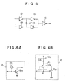
- FIG. 5 there is shown an embodiment of an FM signal demodulation circuit according to the invention which comprises five inverters 12, 13, 14, 15 and 16, and a capacitor 17 connected between output terminals of the inverters 12 and 13.
- an integrated injection logic hereinafter referred to as 1 2 L
- 1 2 L an integrated injection logic
- the injector current source 12i a circuit as exemplified in Fig. 6B by comprising a resistor 121 and a PNP transistor 122. Potentials V 1 and V 2 in this circuit will not be in excess of the base/emitter voltage which is about 0.7 V. Thus, the number of cascaded transistor stages can be regarded as one, and can advantageously be adapted for low voltage operation.
- the FM signal demodulation circuit of Fig. 5 is practiced through the use of the inverters in the form of 1 2 Ls as shown in Fig. 6A. More particularly, currents from injector current sources 12i, 13i, 14i, 15i and 16i are fed to bases of transistors 12a, 13a, 14a, 15a and 16a, respectively.
- a frequency modulated signal A is inputted to the base (input electrode) of the transistor 12a, and a frequency modulated signal B having a phase opposite to that of the frequency modulated signal A is inputted to the base (input electrode) of the transistor 13a.
- the current of the injector current source 12i flows into the transistor 12a to turn on the same, thereby causing an output signal C from its collector (output electrode) to assume a low level.
- the current of the injector current source 12i is drawn into an input terminal f and the transistor 12a is turned off. Consequently, the output signal C from the collector of the transistor 12a assumes a high level.
- the transistor 13a operates in response to the signal B inputted to its base (input electrode) in the same manner as the transistor 12a.
- the collector of the transistor 12a is connected to the base (input electrode) of the transistor 14a and the transistor 13a has its collector (output electrode) connected to the base (input electrode) of the transistor 15a. Between the collectors of the transistors 12a and 13a is connected a capacitor 17. Collectors (output electrodes) of the transistors 14a and 15a are connected in common to the base (input electrode) of the transistor 16a.
- Fig. 8 illustrates signal waveforms appearing at the input and output electrodes of each of the transistors shown in Fig. 7.
- Waveforms of the frequency modulated signals A and B have phases which are opposite to each other, and a pulse height which needs to be in excess of a predetermined voltage V F ( ⁇ 0.6 V).
- the output signal C from the collector of the transistor 12a is.fixed to the low level which is approximately zero volt.
- the frequency modulated signal B assumes the low level. Consequently, the transistor 13a is turned off and the capacitor 17 is charged with the current of the injector current source 15i with the output voltage signal D from the collector of the transistor 13a increased.
- the transistor 15a is turned on so that the voltage of the output signal D is fixed to V F . Sympathetically therewith, the output signal F of the transistor 15a assumes the low level.
- the capacitor 17 is so charged and maintained as to hold the output signal C at zero volt and the output signal D at +V F .
- the transistor 12a When, on the other hand, the frequency modulated signal A changes from high to low with the frequency modulated signal B changed from low to high, the transistor 12a is turned off and the transistor 13a is turned on with the output signal D fixed to zero volt.
- the capacitor 17 is charged with the current from the injector current source 14i until the voltage of the output signal C reaches +V F at which the transistor 14a is turned on.
- the output voltage signal C is then fixed to +V F with the output signal E from the collector of the transistor 14a lowered.
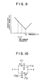
- the time, T required for changing the voltage of the output signal C from -V F to +V F is given by the following equation (2): where Id is a constant current from the injector current source 14i, and Cd is a capacitance of the capacitor 17.
- the time required for changing the voltage of the output signal D from -V F to +V F also measures T pursuant to equation (2), provided that Id therein is interpreted as a constant current from the injector current source 15i.
- T is determined by a time constant of an impedance R on the injector current sources and the capacitance of the capacitor 17.
- the output signal E from the collector of the transistor 14a and the output signal F from the collector of the transistor 15a are ANDed and applied to the base of the transistor 16a which in turn produces from its collector the output signal G in the form of a wave of expansion having a pulse width T as shown in Fig. 8.
- This output signal G is passed through a low-pass filter 18 to provide a demodulated signal v on an output terminal 19.
- the waveforms of the output signals E and F are those occurring prior to the logical product operation.
- the demodulation circuit according to this embodiment is of a differential type which can substantially zero the delay time differences between the inverters 12 and 13 and between the inverters 14 and 15, and that the injector currents of the injector current sources 14i and 15i can be set to be equal to each other since the injector current sources 14i and 15i can be adjusted independently of the injector current sources 12i, 13i and 16i, time dependent variations of the delay time T can be minimized to thereby suppress the carrier leakage to an extremely small level.
- the aforementioned delay time T must be set to a prescribed value which satisfies
- this value of the delay time T varies with irregularity in capacitance of the capacitor 17 and capacitances of parasitic base capacitors (not shown) of the transistors 14a and 15a or dependent on temperature characteristics of active elements used. Therefore, adjustment or temperature characteristic correction is effected in respect of the injector current sources 14i and 15i so as to set the delay time T to the prescribed value.
- parasitic capacitors 171S and 172S between the capacitor 17 and a substrate must be taken into consideration and accordingly, a metal side M and a substrate side S of either of two MOS capacitors 171 and 172 each having an equal capacitance must be connected in back to back relationship in order not to disturb the differential type configuration.
- the dealy times for the individual transistors 12a and 13a vary with irregularity in parasitic capacitors (not shown) associated with the respective transistors and in currents from the injector current sources 12i and 13i, but the relative difference between those delay times can be zeroed to obviate the problem of the carrier leakage.
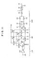
- Fig. 11 shows an interface INT interposed between a linear circuit LIN and the FM signal demodulation circuit DEM according to this invention which takes the form of an integrated injection logic.
- a frequency modulated signal 23 is applied to an amplifier 20.
- Inverters 21 and 22 used as buffer amplifiers do not incorporate dedicated injector current sources.
- Reference characters Q 1 to Q 12 denote transistors and like reference numerals designate like elements in Fig. 7.
- the frequency modulated signal 23 is passed through the amplifier 20 and then applied to the transistors Q l and Q 2 constituting a differential amplifier.
- the transistors Q 3 , Q 4 , Q 5 , Q 9 and Q 10 are rendered on and the transistors Q 6 , Q 7 , Q 8 , Q 11 and Q 12 are rendered off to apply a high-level input signal to the inverter 21 and a low- level input signal to the inverter 22.
- Fig. 12 illustrates another embodiment of the FM signal demodulation circuit according to the present invention. This embodiment is different from the Fig. 5 embodiment in that in place of the capacitor 17 connected between the output terminals of the inverters 12 and 13, there are provided a capacitor 24 connected between the output terminal of the inverter 12 and ground and a capacitor 25 connected between the output terminal of the inverter 13 and ground.
- V B aims at prevention of saturation of the P NP transistor 262 with promising high speed operation ensured.
- An NPN transistor 26a plays the part of the transistor 12a shown in Fig. 6B.
- a resistor 261 also plays the part of the resistor 121 of Fig. 6B.
- the NPN transistor 26a may be a Schottky type transistor which is effective to prevent itself from being saturated.
- potential V 3 is given by the following equation (4): and when V B is selected to be about 0.7 V, the number of cascaded transistor stages is regarded as about two, which is compatible with low voltage operation. However, as far as the low voltage operation is concerned, the I 2 L inverter is more advantageous.
- the I 2 L inverter has a device area which is about 1/3 of a device area of the conventional transistor inverter. Accordingly, by applying the I 2 L inverters to the FM signal demodulation circuit, the area thereof can be reduced as compared to the area of the conventional FM signal demodulation circuit. As well known in the art, the reduction in the area of IC devices contributes to reduction in manufacture cost. Consequently, the FM signal demodulation circuit can be manufactured at low cost.
Landscapes
- Engineering & Computer Science (AREA)
- Power Engineering (AREA)
- Television Signal Processing For Recording (AREA)
- Manipulation Of Pulses (AREA)
Applications Claiming Priority (2)
| Application Number | Priority Date | Filing Date | Title |
|---|---|---|---|
| JP58066954A JPS59193609A (ja) | 1983-04-18 | 1983-04-18 | Fm復調回路 |
| JP66954/83 | 1983-04-18 |
Publications (2)
| Publication Number | Publication Date |
|---|---|
| EP0122632A2 true EP0122632A2 (de) | 1984-10-24 |
| EP0122632A3 EP0122632A3 (de) | 1989-02-22 |
Family
ID=13330920
Family Applications (1)
| Application Number | Title | Priority Date | Filing Date |
|---|---|---|---|
| EP84104334A Withdrawn EP0122632A3 (de) | 1983-04-18 | 1984-04-17 | Schaltungsanordnung zur Demodulation eines FM-Signales |
Country Status (3)
| Country | Link |
|---|---|
| US (1) | US4591798A (de) |
| EP (1) | EP0122632A3 (de) |
| JP (1) | JPS59193609A (de) |
Families Citing this family (2)
| Publication number | Priority date | Publication date | Assignee | Title |
|---|---|---|---|---|
| JPS61246749A (ja) * | 1985-04-24 | 1986-11-04 | Konishiroku Photo Ind Co Ltd | ハロゲン化銀写真感光材料 |
| JPS61250643A (ja) | 1985-04-30 | 1986-11-07 | Konishiroku Photo Ind Co Ltd | ハロゲン化銀写真感光材料 |
Family Cites Families (4)
| Publication number | Priority date | Publication date | Assignee | Title |
|---|---|---|---|---|
| US3121202A (en) * | 1961-03-07 | 1964-02-11 | Gen Precision Inc | Sine-cosine frequency tracker |
| GB1437325A (en) * | 1972-08-18 | 1976-05-26 | Rca Corp | Fm demodulator |
| JPS54158153A (en) * | 1978-06-02 | 1979-12-13 | Nec Corp | Fm demodulating circuit |
| US4471312A (en) * | 1981-06-02 | 1984-09-11 | Texas Instruments Incorporated | Integrated circuit demodulator for FSK signals |
-
1983
- 1983-04-18 JP JP58066954A patent/JPS59193609A/ja active Granted
-
1984
- 1984-04-17 EP EP84104334A patent/EP0122632A3/de not_active Withdrawn
- 1984-04-17 US US06/601,290 patent/US4591798A/en not_active Expired - Fee Related
Also Published As
| Publication number | Publication date |
|---|---|
| JPS59193609A (ja) | 1984-11-02 |
| JPH0122765B2 (de) | 1989-04-27 |
| EP0122632A3 (de) | 1989-02-22 |
| US4591798A (en) | 1986-05-27 |
Similar Documents
| Publication | Publication Date | Title |
|---|---|---|
| US3602737A (en) | Circuit arrangement for reduction of high frequency noise disturbances in wide bandsignals such as video signals | |
| JPS614310A (ja) | レベルシフト回路 | |
| US4724405A (en) | Modulator | |
| US4591798A (en) | FM signal demodulation circuit | |
| US3783398A (en) | Fm pulse averaging demodulator | |
| US4636745A (en) | Signal waveform equalizing circuitry | |
| US4634995A (en) | Electronic circuitry utilizing an inerted Darlington amplifier output stage to be operable with a low supply voltage | |
| US4280100A (en) | Time modulation pulse averaging demodulator | |
| US5317414A (en) | Drop out compensation circuit | |
| JPS6238375Y2 (de) | ||
| KR900004623B1 (ko) | 비디오 신호재생장치의 fm휘도신호의 복조장치 | |
| JPS5949728B2 (ja) | 可変インピ−ダンス回路 | |
| JP3355632B2 (ja) | レベル制御回路 | |
| JPS6340896Y2 (de) | ||
| JPS5941637B2 (ja) | 色信号処理装置 | |
| JPS622850Y2 (de) | ||
| JPH0411426Y2 (de) | ||
| JP2531789B2 (ja) | ホワイト・ダ―ククリップ回路 | |
| JPS61295701A (ja) | 差動増幅回路型検波器 | |
| JPS6250018B2 (de) | ||
| JPH0123989B2 (de) | ||
| JPS6336568B2 (de) | ||
| JPH051677B2 (de) | ||
| JPS601921A (ja) | アナログ・スイツチ回路 | |
| JPH01168106A (ja) | 周波数補正回路 |
Legal Events
| Date | Code | Title | Description |
|---|---|---|---|
| PUAI | Public reference made under article 153(3) epc to a published international application that has entered the european phase |
Free format text: ORIGINAL CODE: 0009012 |
|
| 17P | Request for examination filed |
Effective date: 19840417 |
|
| AK | Designated contracting states |
Designated state(s): DE FR GB IT |
|
| PUAL | Search report despatched |
Free format text: ORIGINAL CODE: 0009013 |
|
| AK | Designated contracting states |
Kind code of ref document: A3 Designated state(s): DE FR GB IT |
|
| 17Q | First examination report despatched |
Effective date: 19900809 |
|
| STAA | Information on the status of an ep patent application or granted ep patent |
Free format text: STATUS: THE APPLICATION HAS BEEN WITHDRAWN |
|
| 18W | Application withdrawn |
Withdrawal date: 19910227 |
|
| RIN1 | Information on inventor provided before grant (corrected) |
Inventor name: KOBORI, YASUNORI Inventor name: SHIOMI, MAKOTO Inventor name: FUKUSHIMA, ISAO Inventor name: MIURA, KUNIAKI Inventor name: KANO, KENJI |