EP0122984B1 - Circuit de mesure de temps - Google Patents
Circuit de mesure de temps Download PDFInfo
- Publication number
- EP0122984B1 EP0122984B1 EP83302263A EP83302263A EP0122984B1 EP 0122984 B1 EP0122984 B1 EP 0122984B1 EP 83302263 A EP83302263 A EP 83302263A EP 83302263 A EP83302263 A EP 83302263A EP 0122984 B1 EP0122984 B1 EP 0122984B1
- Authority
- EP
- European Patent Office
- Prior art keywords
- clock pulse
- gate signal
- signal
- output
- measuring circuit
- Prior art date
- Legal status (The legal status is an assumption and is not a legal conclusion. Google has not performed a legal analysis and makes no representation as to the accuracy of the status listed.)
- Expired
Links
- 230000010354 integration Effects 0.000 claims description 16
- 230000000737 periodic effect Effects 0.000 claims description 14
- 230000005540 biological transmission Effects 0.000 claims description 13
- 230000001419 dependent effect Effects 0.000 claims description 2
- 238000005259 measurement Methods 0.000 description 5
- 238000010586 diagram Methods 0.000 description 4
- 230000004304 visual acuity Effects 0.000 description 4
- 230000008034 disappearance Effects 0.000 description 3
- 230000004048 modification Effects 0.000 description 3
- 238000012986 modification Methods 0.000 description 3
- 230000000694 effects Effects 0.000 description 2
- 239000000523 sample Substances 0.000 description 2
- 230000004913 activation Effects 0.000 description 1
- 230000006978 adaptation Effects 0.000 description 1
- 230000004323 axial length Effects 0.000 description 1
- 238000006243 chemical reaction Methods 0.000 description 1
- 239000013078 crystal Substances 0.000 description 1
- 230000004069 differentiation Effects 0.000 description 1
Images


Classifications
-
- G—PHYSICS
- G04—HOROLOGY
- G04F—TIME-INTERVAL MEASURING
- G04F10/00—Apparatus for measuring unknown time intervals by electric means
Definitions
- the present invention relates to a time measuring circuit for meters of the pulse reflection type such as an ultrasonic axial force meter, an ultrasonic thickness meter or the like.
- a time measuring circuit for use in meters of the pulse reflection type for measuring a parameter of an object, the circuit including: a pulse oscillator means for producing a clock pulse at a predetermined frequency; means for producing a transmission pulse signal for transmission to the object to be measured; receiving means for receiving an echo pulse signal reflected from said object; a gate signal generator responsive to the transmission and echo pulse signals for producing a gate signal the duration of which is dependent on the time interval to be measured between transmission of the transmission pulse signal and receipt of the echo pulse signal; means responsive to the gate signal and to the clock pulse for providing a periodic waveform; means for detecting the value of the periodic waveform on termination of the gate signal; and means for providing an output related to the duration of the gate signal from a combination of a counted value of pulses and a quantity derived from said detected value the time measuring circuit.
- the first means comprises a complementary-output element responsive to the clock pulse from said oscillator means for producing said first and second clock pulse trains;
- the third means is in the form of a counter connected to the flip-flop to count the pulses of the first clock pulse train
- the second means is in the form of a pair of integration circuits connected to the flip-flop to selectively integrate the first and second clock pulses in response to the gate pulse signal
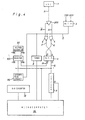
- Fig. 1 illustrates a time measuring circuit adapted to an ultrasonic axial force meter of the pulse reflection type.
- the time measuring circuit includes a crystal oscillator 1 for producing clock pulses A in the form of rectangular waves at a frequency of 100 KHz-10 MHz, and a JK flip-flop 2 connected at its clock terminal CK to the output terminal of oscillator 1 and at its other input terminals J and K to a DC voltage source Vcc.
- the time measuring circuit further includes an RS flip-flop 3 which is applied at its set terminal S with a transmission pulse signal TTP from the ultrasonic axial force meter and at its reset terminal R with a reflection echo pulse RTP from the axial force meter.
- RS flip-flop 3 is connected at its output terminal Q to a clear input terminal CLR of flip-flop 2, each first input terminal of NAND gates 4 and 5, and the input terminal of a timer 8.
- the output terminal Q of RS flip-flop 3 is further connected to each set terminal S of first and second integration circuits 11 and 12 respectively through inverters 9 and 10.
- NAND gates 4 and 5 are connected at their second input terminals to output terminals Q and Q of JK flip-flop 2 and at their output terminals to reset and set terminals R and S of a second flip-flop 6 respectively.
- a first output terminal Q of RS flip-flop 6 is connected to the input terminal of a counter 7, a microcomputer 14 and a reset terminal R of the second integration circuit 12, while a second output terminal Q of RS flip-flop 6 is connected to a reset terminal R of the first integration circuit 11.
- Each output terminal of integration circuits 11 and 12 is connected to an analog-to-digital (or A-D) converter 13 which is in turn connected to microcomputer 14.
- the microcomputer 14 is commercially available, the interface of which is connected at its input terminals to respective output terminals of counter 7, timer 8 and A-D converter 13.
- the ultrasonic axial force meter includes a frequency divider 21 in the form of a counter for dividing the frequency of the clock pulses A from oscillator 1, and a pulse width adjuster 22 in the form of a one-shot circuit or a differentiation circuit for forming rectangular impulse waves from the divided clock pulses.
- the rectangular impulse waves are transmitted to a trigger circuit 23 and also transmitted as the transmission pulse signal TTP to RS flip-flop 3.
- the ultrasonic axial force meter further includes a probe 30 connected to trigger circuit 23 for producing an ultrasonic pulse wave, which is transmitted to an object to be measured, a receiving amplifier 31 for receiving an echo pulse train output from probe 30, and a comparator 32 for comparing an output of the amplifier 31 with a predetermined value to produce the reflection echo pulse RTP.
- the ultrasonic axial force meter includes a reset circuit 24 connected to a reset terminal R of counter 7 and responsive to the divided clock pulses from frequency divider 21 for producing a reset signal in accordance with the clock pulses from oscillator 1, a ten-key board 41 for applying an input signal indicative of a constant of the object such as a bolt to the computer 14, a select- key board 42 for selecting input data for the computer 14, an indicator 43 for indicating a value measured by the computer 14, and a thermometer 44 for measuring a temperature of the object and the ambient temperature.
- RS flip- flop 3 is set in response to the transmission pulse signal TTP to produce a gate signal D at a high level and is reset in response to the reflection echo pulse RTP to make the gate signal low level.
- the duration of gate signal D is proportional, for instance, to an axial length of the bolt to be measured.
- the gate signal D causes JK flip-flip 2 to divide clock pulses A from oscillator 1 to produce at its terminals Q and Q output signals B, C in the form of rectangular waves which are relatively inverted at half the frequency of the clock pulses.
- the level of gate signal D becomes low, the output signal B from terminal Q is maintained at a high level, while the output signal C from terminal Q is maintained at a low level.
- NAND gates 4 and 5 are responsive to the gate signal D to permit the output signals B and C to be applied to the second RS flip-flop 6 from JK flip-flop 2.
- the timer 8 produces a high level signal therefrom after lapse of a time t
- the computer 14 is responsive to the high level signal from timer 8 to receive output signals from counter 7 and A-D converter 13, as is described in detail later.
- the output signals B and C from JK flip-flop 2 are relatively inverted to form the output signals E and F from NAND gates 4 and 5 during appearance of the gate signal D.
- the output signals E and F are maintained at a high level respectively.
- the second RS flip-flop 6 is applied at its terminals R and S with relatively inverted output signals E and F during appearance of the gate signal D, it produces relatively inverted output signals G and H at its terminals Q and Q. Upon disappearance of the gate signal D, the second RS flip-flop 6 acts to store each level of the output signals E and F.
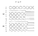
- the output signal G from RS flip-flop 6 is applied as an input signal with a high level to the counter 7, as is illustrated in (a) of Figure 3. If the level of gate signal D becomes low when the output signals B and C from JK flip-flop 2 are at high and low levels respectively, the output signal G from RS flip-flop 6 is applied as an input signal with a low level to the counter 7, as is illustrated in (b) of Figure 3. As a result, the counter 7 acts to count the number of the output pulses G from RS flip-flop 6 thereby to measure a timely. Furthermore, the computer 14 discriminates the operation of integration circuit 11 or 12 in relation to the level of the output signal G from RS flip-flop 6 to produce an output signal therefrom for activation of A-D converter 13.
- the first integration circuit 11 When applied with the output signal H at a low level from RS flip-flop 6, the first integration circuit 11 operates to produce an output signal I in the form of saw tooth waves.
- A-D converter 13 is responsive to the output signal from computer 14 to convert the final voltage level of output signal I into a digital value indicative of a time T 2 .
- the time T 2 is measured by a digital value converted from the final saw tooth wave of signal I. This means that resolution or resolving power in measurement of the time T 2 can easily be enhanced up to e.g. 1 nS, in dependence on the capacity of the A-D converter 13 related to the frequency of the clock pulses.
- the second integration circuit 12 When applied with the output signal G with the low level from RS flip-flop 6, as is illustrated in (b) of Figure 3, the second integration circuit 12 operates to produce an output signal J in the form of saw tooth waves.
- A-D converter 13 is responsive to the output signal from computer 14 to convert the final voltage level of output signal J into a digital value indicative of a time T 3 . This means that resolution or resolving power in measurement of the time T 3 can be easily enhanced up to, e.g., 1 nS, in dependence on the capacity of the A-D converter 13 related to the frequency of the clock pulses.
- integration circuits 11 and 12 startto integrate the low levels of input signals H and G applied to their reset terminals R respectively during appearance of the gate signal D and discharge when the levels of the input signals H and G become high.
- the integration circuits 11 and 12 act to hold therein the finally integrated voltages respectively, and subsequently A-D converter 13 is activated in response to the output signal from computer 14 in relation to the level of the output signal G to convert the integrated voltage into the digital value and produces an output signal indicative of the digital value upon completion of the voltage conversion.
- the computer 14 receives an output signal from counter 7 to measure a sum of the time T, and the time T 2 or T 2 and T 3 , and the counter 7 is reset by a reset signal from reset circuit 24.
- the microcomputer 14 In the case that the microcomputer 14 is applied with the input signal G with high level upon disappearance of the gate signal D, it measures the time T on the basis of the following equation:
- the microcomputer 14 In the case that the microcomputer 14 is applied with the input signal G with low level upon disappearance of the gate signal D, it measures the time T on a basis of the following equation-: where the value of T 2 is determined in its full scale.
- FIG 4 there is illustrated a modification of the time measuring circuit described above, in which JK flip-flop 2 in Figure 1 is replaced with a complementary-output element 200, and the integration circuits 11 and 12 are replaced with a voltage generator 90, a selector 100 and a single integration circuit 110.
- the complementary-output element 200 is arranged to produce relatively inverted clock pulses A and A at the same phase in response to input clock pulses from oscillator 1.
- the voltage generator 90 is arranged to produce positive and negative voltage signals +V s , -V s which have the same voltage levels and different polarities
- the selector 100 is, for example, in the form of an analogue switch which is connected to voltage generator 90 to produce a positive voltage signal +Vg in response to the low level signal H from RS flip-flop 6 and to produce a negative voltage signal -V s in response to the low level signal G from RS flip-flop 6, and the integration circuit 110 is arranged to charge in response to the positive voltage signal +V s and discharge in response to the negative voltage signal -V s thereby to produce an output signalla in the form of triangular waves as is illustrated in Fig. 5.
- the other arrangements are substantially the same as those in the time measuring circuit of Fig. 1.
- A-D converter 13 of the above embodiment may be replaced with a voltage-frequency converter with a counter.
Landscapes
- Physics & Mathematics (AREA)
- General Physics & Mathematics (AREA)
- Measurement Of Unknown Time Intervals (AREA)
- Radar Systems Or Details Thereof (AREA)
- Measurement Of Velocity Or Position Using Acoustic Or Ultrasonic Waves (AREA)
Claims (7)
Priority Applications (2)
| Application Number | Priority Date | Filing Date | Title |
|---|---|---|---|
| EP83302263A EP0122984B1 (fr) | 1983-04-21 | 1983-04-21 | Circuit de mesure de temps |
| DE8383302263T DE3377748D1 (en) | 1983-04-21 | 1983-04-21 | Time measuring circuit |
Applications Claiming Priority (1)
| Application Number | Priority Date | Filing Date | Title |
|---|---|---|---|
| EP83302263A EP0122984B1 (fr) | 1983-04-21 | 1983-04-21 | Circuit de mesure de temps |
Publications (2)
| Publication Number | Publication Date |
|---|---|
| EP0122984A1 EP0122984A1 (fr) | 1984-10-31 |
| EP0122984B1 true EP0122984B1 (fr) | 1988-08-17 |
Family
ID=8191127
Family Applications (1)
| Application Number | Title | Priority Date | Filing Date |
|---|---|---|---|
| EP83302263A Expired EP0122984B1 (fr) | 1983-04-21 | 1983-04-21 | Circuit de mesure de temps |
Country Status (2)
| Country | Link |
|---|---|
| EP (1) | EP0122984B1 (fr) |
| DE (1) | DE3377748D1 (fr) |
Families Citing this family (3)
| Publication number | Priority date | Publication date | Assignee | Title |
|---|---|---|---|---|
| JPH0820473B2 (ja) * | 1987-02-04 | 1996-03-04 | 株式会社 アドバンテスト | 連続的周期−電圧変換装置 |
| DE4222643A1 (de) * | 1992-07-10 | 1994-01-13 | Bodenseewerk Geraetetech | Einrichtung zur Messung von Pulslaufzeiten |
| JP6299516B2 (ja) * | 2014-08-05 | 2018-03-28 | 株式会社デンソー | 時間計測回路 |
Family Cites Families (1)
| Publication number | Priority date | Publication date | Assignee | Title |
|---|---|---|---|---|
| JPS52123670A (en) * | 1976-04-09 | 1977-10-18 | Takeda Riken Ind Co Ltd | Digital frequency measuring device |
-
1983
- 1983-04-21 EP EP83302263A patent/EP0122984B1/fr not_active Expired
- 1983-04-21 DE DE8383302263T patent/DE3377748D1/de not_active Expired
Non-Patent Citations (2)
| Title |
|---|
| IBM TECHNICAL DISCLOSURE BULLETIN, vol. 4, no. 5, October 1961, New York (US), J. DIAZ: "Radar pulse measuring", p. 27 * |
| IEEE TRANSACTIONS ON INSTRUMENTATION AND MEASUREMENT, vol. IM-21, no. 4, November 1972, R.A. BENSON et al.: "The folded ramp: A new technique for computer-controlled time-interval measurement", p. 409-412 * |
Also Published As
| Publication number | Publication date |
|---|---|
| EP0122984A1 (fr) | 1984-10-31 |
| DE3377748D1 (en) | 1988-09-22 |
Similar Documents
| Publication | Publication Date | Title |
|---|---|---|
| US3985022A (en) | Ultrasonic thickness measuring method and apparatus | |
| US4637733A (en) | High-resolution electronic chronometry system | |
| US4168467A (en) | Measurement of pulse duration | |
| US4598375A (en) | Time measuring circuit | |
| US4912962A (en) | Method of detection of oscillation period for oscillatory densimeter | |
| EP0122984A1 (fr) | Circuit de mesure de temps | |
| US3717033A (en) | Ultrasonic apparatus, particularly for thermometry | |
| JPS6324273B2 (fr) | ||
| SU949623A1 (ru) | Измеритель центра пр моугольного импульса | |
| SU976396A1 (ru) | Цифровой частотомер | |
| GB2102226A (en) | Analog to digital converter | |
| SU464887A1 (ru) | Измеритель временных интервалов | |
| SU1596269A1 (ru) | Цифровой низкочастотный фазометр | |
| SU1525606A1 (ru) | Устройство дл измерени расхождени периодов у двух импульсных генераторов с близкими частотами | |
| SU849096A1 (ru) | Фазометр | |
| SU847032A1 (ru) | Ультразвуковой толщиномер | |
| SU817605A1 (ru) | Цифровой фазометр | |
| SU957121A1 (ru) | Измеритель средней частоты следовани импульсов | |
| SU734591A1 (ru) | Устройство измерени параметров морского волнени | |
| SU868695A1 (ru) | Двухшкальный измеритель временных интервалов | |
| SU690405A2 (ru) | Цифровой процентный частотомер | |
| SU993142A1 (ru) | Измеритель отношени частот | |
| SU555342A1 (ru) | Устройство дл измерени скорости вращени | |
| SU556325A1 (ru) | Устройство дл измерени непрерывных физических величин | |
| RU1798727C (ru) | Способ определени фазового сдвига объекта |
Legal Events
| Date | Code | Title | Description |
|---|---|---|---|
| PUAI | Public reference made under article 153(3) epc to a published international application that has entered the european phase |
Free format text: ORIGINAL CODE: 0009012 |
|
| AK | Designated contracting states |
Designated state(s): DE GB SE |
|
| 17P | Request for examination filed |
Effective date: 19850419 |
|
| 17Q | First examination report despatched |
Effective date: 19860604 |
|
| D17Q | First examination report despatched (deleted) | ||
| GRAA | (expected) grant |
Free format text: ORIGINAL CODE: 0009210 |
|
| AK | Designated contracting states |
Kind code of ref document: B1 Designated state(s): DE GB SE |
|
| REF | Corresponds to: |
Ref document number: 3377748 Country of ref document: DE Date of ref document: 19880922 |
|
| PLBE | No opposition filed within time limit |
Free format text: ORIGINAL CODE: 0009261 |
|
| STAA | Information on the status of an ep patent application or granted ep patent |
Free format text: STATUS: NO OPPOSITION FILED WITHIN TIME LIMIT |
|
| 26N | No opposition filed | ||
| EAL | Se: european patent in force in sweden |
Ref document number: 83302263.5 |
|
| PGFP | Annual fee paid to national office [announced via postgrant information from national office to epo] |
Ref country code: GB Payment date: 19950419 Year of fee payment: 13 |
|
| PGFP | Annual fee paid to national office [announced via postgrant information from national office to epo] |
Ref country code: SE Payment date: 19950425 Year of fee payment: 13 |
|
| PGFP | Annual fee paid to national office [announced via postgrant information from national office to epo] |
Ref country code: DE Payment date: 19950523 Year of fee payment: 13 |
|
| PG25 | Lapsed in a contracting state [announced via postgrant information from national office to epo] |
Ref country code: GB Effective date: 19960421 |
|
| PG25 | Lapsed in a contracting state [announced via postgrant information from national office to epo] |
Ref country code: SE Effective date: 19960422 |
|
| GBPC | Gb: european patent ceased through non-payment of renewal fee |
Effective date: 19960421 |
|
| PG25 | Lapsed in a contracting state [announced via postgrant information from national office to epo] |
Ref country code: DE Effective date: 19970101 |
|
| EUG | Se: european patent has lapsed |
Ref document number: 83302263.5 |