EP0123093A1 - Schottky-Diode, integrierte Schaltung mit Schottky-Diode und Verfahren zur Herstellung derselben - Google Patents
Schottky-Diode, integrierte Schaltung mit Schottky-Diode und Verfahren zur Herstellung derselben Download PDFInfo
- Publication number
- EP0123093A1 EP0123093A1 EP84102643A EP84102643A EP0123093A1 EP 0123093 A1 EP0123093 A1 EP 0123093A1 EP 84102643 A EP84102643 A EP 84102643A EP 84102643 A EP84102643 A EP 84102643A EP 0123093 A1 EP0123093 A1 EP 0123093A1
- Authority
- EP
- European Patent Office
- Prior art keywords
- layer
- schottky
- buried
- diode
- surface layer
- Prior art date
- Legal status (The legal status is an assumption and is not a legal conclusion. Google has not performed a legal analysis and makes no representation as to the accuracy of the status listed.)
- Withdrawn
Links
Images

Classifications
-
- H—ELECTRICITY
- H10—SEMICONDUCTOR DEVICES; ELECTRIC SOLID-STATE DEVICES NOT OTHERWISE PROVIDED FOR
- H10P—GENERIC PROCESSES OR APPARATUS FOR THE MANUFACTURE OR TREATMENT OF DEVICES COVERED BY CLASS H10
- H10P30/00—Ion implantation into wafers, substrates or parts of devices
- H10P30/20—Ion implantation into wafers, substrates or parts of devices into semiconductor materials, e.g. for doping
- H10P30/21—Ion implantation into wafers, substrates or parts of devices into semiconductor materials, e.g. for doping of electrically active species
-
- H—ELECTRICITY
- H10—SEMICONDUCTOR DEVICES; ELECTRIC SOLID-STATE DEVICES NOT OTHERWISE PROVIDED FOR
- H10D—INORGANIC ELECTRIC SEMICONDUCTOR DEVICES
- H10D8/00—Diodes
- H10D8/60—Schottky-barrier diodes
-
- H—ELECTRICITY
- H10—SEMICONDUCTOR DEVICES; ELECTRIC SOLID-STATE DEVICES NOT OTHERWISE PROVIDED FOR
- H10D—INORGANIC ELECTRIC SEMICONDUCTOR DEVICES
- H10D84/00—Integrated devices formed in or on semiconductor substrates that comprise only semiconducting layers, e.g. on Si wafers or on GaAs-on-Si wafers
- H10D84/01—Manufacture or treatment
-
- H—ELECTRICITY
- H10—SEMICONDUCTOR DEVICES; ELECTRIC SOLID-STATE DEVICES NOT OTHERWISE PROVIDED FOR
- H10P—GENERIC PROCESSES OR APPARATUS FOR THE MANUFACTURE OR TREATMENT OF DEVICES COVERED BY CLASS H10
- H10P30/00—Ion implantation into wafers, substrates or parts of devices
- H10P30/20—Ion implantation into wafers, substrates or parts of devices into semiconductor materials, e.g. for doping
- H10P30/202—Ion implantation into wafers, substrates or parts of devices into semiconductor materials, e.g. for doping characterised by the semiconductor materials
- H10P30/206—Ion implantation into wafers, substrates or parts of devices into semiconductor materials, e.g. for doping characterised by the semiconductor materials into Group III-V semiconductors
-
- H—ELECTRICITY
- H10—SEMICONDUCTOR DEVICES; ELECTRIC SOLID-STATE DEVICES NOT OTHERWISE PROVIDED FOR
- H10P—GENERIC PROCESSES OR APPARATUS FOR THE MANUFACTURE OR TREATMENT OF DEVICES COVERED BY CLASS H10
- H10P30/00—Ion implantation into wafers, substrates or parts of devices
- H10P30/20—Ion implantation into wafers, substrates or parts of devices into semiconductor materials, e.g. for doping
- H10P30/22—Ion implantation into wafers, substrates or parts of devices into semiconductor materials, e.g. for doping using masks
-
- H—ELECTRICITY
- H10—SEMICONDUCTOR DEVICES; ELECTRIC SOLID-STATE DEVICES NOT OTHERWISE PROVIDED FOR
- H10P—GENERIC PROCESSES OR APPARATUS FOR THE MANUFACTURE OR TREATMENT OF DEVICES COVERED BY CLASS H10
- H10P30/00—Ion implantation into wafers, substrates or parts of devices
- H10P30/20—Ion implantation into wafers, substrates or parts of devices into semiconductor materials, e.g. for doping
- H10P30/28—Ion implantation into wafers, substrates or parts of devices into semiconductor materials, e.g. for doping characterised by an annealing step, e.g. for activation of dopants
Definitions
- the invention relates to semiconductor diodes and in particular integrable Schottky diodes with low resistance, which can be operated at millimeter wave frequencies.
- the invention characterized in the claims serves to solve this problem;
- the object of the invention is therefore to provide a corresponding diode structure which meets the stated requirement and a method for its production.
- a Schottky diode structure which is arranged in a compound semiconductor substrate and consists of a buried layer of n -conducting material which is overlaid by a surface layer of weakly doped n -conducting material, a Schottky contact are connected to the surface and an ohmic contact to the buried layer.
- the invention further describes the provision of an integrated circuit that operates in the millimeter-wave range and includes a Schottky field effect transistor (MES field effect transistor) and a Schottky diode structure formed in a compound semiconductor substrate.
- the circuit contains a buried layer of n -conducting material, superimposed by a surface layer of weakly n-doped material, a Schottky diode contact and a Schottky gate contact arranged on the surface, as well as first, second and third ohmic contacts the buried layer, which represents the ohmic contact of the diode and the source and drain contacts of the MES field-effect transistor.
- the invention further provides a method of making a semiconductor structure including a Schottky diode in a compound semiconductor substrate, the method including selectively implanting high energy ions into the substrate to form a buried layer of n + - conductive material, furthermore the implantation of ions with low energy to form a surface layer of weakly n-conducting material, as well as the formation of a Schottky contact on the surface layer and an ohmic contact on the buried layer.
- a suitable compound semiconductor material is gallium arsenide, since it has a band gap suitable for generating high frequencies and corresponding carrier mobility; the preferred manufacturing technique uses the implantation of doubly charged n-doped ions, such as silicon, at high energy to produce the highly doped buried layer of the n + type . Subsequent low energy implantation provides a lightly doped n-type surface layer on which the Schottky contact of the diode is then formed.
- the selective implantation of the buried layer enables a structure with low parasitic capacitance and accordingly improved behavior at high frequencies to be achieved.
- the technology is compatible with the current MESFET process and is therefore particularly suitable for the production of integrated circuits that operate in the miRimeter wave range.
- the Schottky diode is formed in a compound semiconductor substrate, advantageously: as part of an integrated circuit. For the purpose of explanation, only the manufacture of a diode and an adjacent transistor (MESFET) is shown.
- the compound semiconductor substrate 11 (FIG. 1) is provided with the mask 12 and is then the Exposed to high energy doping ion beam to form a buried n-type layer from zones 13 and 13a.
- the substrate characteristically consists of gallium arsenide and the dopant consists of silicon, which is preferred because of its great depth of penetration. With double charged silicon ions and an acceleration voltage of 200 V, corresponding to an energy of 400 KeV, a penetration depth of 0.5 to 0.6 mm can be achieved in the gallium arsenide substrate.
- the n -conducting layer is separated from the semiconductor surface by the weakly doped surface layer 15.
- Their strength is of course a function of the implantation energy and is 0.1 to 0.2 ⁇ m.
- the mask 12 is removed and a second mask 14 (FIG. 2) is applied.
- An implantation of, for example, silicon with low energy (80 KeV, 4 ⁇ 10 12 atoms / cm 3 ) causes an increase in the doping level of the surface layer 15 in the regions 16 in which ohmic contacts are to be formed.
- the doping process determines the channel of the field effect transistor (weakly n-conducting zone 17).
- Mask 14 is removed and the structure is annealed to activate the implanted area.
- the ohmic contacts 21, 22 and 23 are then attached to the n + - conductive zones to form the corresponding ohmic contacts of the Schottky diode 41 and the source and drain contact of the MOS field-effect transistor 42.
- the contacts consist of a lower layer 31 made of gold / germanium alloy and an upper layer 32 made of nickel.
- the Schottky contacts 24, 25 consist of a layer 33 made of chrome and an upper layer 34 made of gold and are attached to the weakly n-doped zones to form the corresponding gate of the MES field-effect transistor and the Schottky contacts of the diode.
- the Schottky contact 25 also lies over a non-implanted area with the formation of interconnections and passive microwave components such as filters, couplers and transmission lines.
- the structure of the Schottky diode is shown in FIG. 5. It can be seen that the ohmic contact 20 and the Schottky contact 25 are arranged side by side on the semiconductor substrate. The edges of the contacts are advantageously designed as interdigitated fingers. This causes the diode structure to break open into a multiplicity of smaller diodes which are connected to one another in parallel, as a result of which the parallel capacitance of the component is substantially reduced.
- the diode structure characteristically comprises at least 10 of these smaller diodes, each of which has a size of approximately 1 ⁇ 2 ⁇ m.
- the series resistance of the diode is low, so that work can be carried out in high frequency ranges.
- the preceding description relates to the manufacture of a diode structure as part of an integrated circuit, but the diode can also be manufactured as a discrete component. Likewise, any other desired compound semiconductor can be used as the preferred material instead of GalLium arsenide.
- the substrate is 11 nm with a thin, 3 x 1 0 3 to 5 x 10 3, preferably coated 4 x 10 3 nm thick surface layer of titanium.
- the photoresist mask 12 is then formed on this layer.
- the purpose of the titanium layer is to prevent any contamination that could result from the contact of the photomask 12 with the semiconductor surface.
- the titanium layer is applied by vapor deposition and is removed by conventional wet etching after the implantation step.
Landscapes
- Junction Field-Effect Transistors (AREA)
- Electrodes Of Semiconductors (AREA)
Abstract
Eine im Hochfrequenzbereich, z.B. im Milimeterwellenbereich arbeitende Halbleiterstruktur, z.B. eine Schottky-Dioden-struktur enthält eine vergrabene Schicht (29) aus n+ -leitendem Material und eine Oberflächenschicht (20) aus schwach n-dotiertem Material, auf der eine ein Schottky-Kontakt (25) angeordnet ist. Die n+ -leitende Schicht sorgt für einen niedrigen Reihenwiderstand, so daß bei hohen Frequenzbereichen gearbeitet werden kann. Die Struktur ist mit dem Herstellverfahren für MES-Feldeffekttransistoren kompatibel und läßt sich somit in eine integrierte Schaltung einbauen.
Description
- Die Erfindung betrifft Halbleiterdioden und insbesondere integrierbare Schottky-Dioden mit niedrigem Widerstand, die bei Millimeterwellenfrequenzen betrieben werden können.
- Mit der steigenden Verwendung von Schaltungen, die im Millimeterwellenbereich arbeiten, z.B. für Fernmeldezwecke, ergibt sich ein Bedarf an Mischerdiodenstrukturen,die in diesen Frequenzbereichen wirkungsvoll arbeiten. Den herkömmlichen Bauelementen haftet der Nachteil an, daß sie einen relativ hohen Reihenwiderstand und/oder eine verhältnismäßig hohe parasitäre Kapazität aufweisen; beides kann ernsthaft den Betrieb im hohen Frequenzbereich beeinträchtigen. Es wurden deshalb eine ganze Reihe von Versuchen zur Schaffung von Diodenstrukturen unternommen, denen diese Nachteile nicht anhaften, aber keine dieser Strukturen ist ohne weiteres mit den MESFET-Herstellungsverfahren kompatibel, die bei der Herstellung von integrierten Schaltungen verwendet werden, die im MiRimeterwellenfrequenzbereich arbeiten.
- Die in den Ansprüchen gekennzeichnete Erfindung dient der Lösung dieser Problemstellung; die Aufgabe der Erfindung besteht demnach darin, eine entsprechende Diodenstruktur, die der genannten Voraussetzung entspricht, sowie ein Verfahren zu deren Herstellung anzugeben.
- Gemäß einem Merkmal der vorliegenden Erfindung wird eine in einem Verbindungshalbleiter-Substrat angeordnete Schottky-Diodenstruktur geschaffen, die aus einer vergrabenen Schicht aus n -leitendem Material besteht, das von einer Oberflächenschicht aus schwach dotiertem n-leitendem Material überlagert ist, wobei ein Schottky-Kontakt an der Oberfläche und ein ohmscher Kontakt an der vergrabenen Schicht angeschlossen sind.
- Die Erfindungbeschreibt ferner die Schaffung einer integrierten Schaltung, die im Millimeterwellenbereich arbeitet und einen Schottky-Feldeffekttransistor (MES-Peldeffekttransistor) und eine Schottky-Diodenstruktur umfaßt, die in einem Verbindungshalbleiter-Substrat ausgebildet sind. Die Schaltung enthält eine vergrabene Schicht aus n -leitendem Material, überlagert von einer Oberflächenschicht aus schwach n-dotiertem Material, einem Schottky-Diodenkontakt und einem Schottky-Gate-Kontakt,angeordnet auf der Oberfläche, sowie ferner erste, zweite und dritte ohmsche Kontakte an der vergrabenen Schicht, die den ohmschen Kontakt der Diode sowie die Source- und Drain-Kontakte des MES-Feldeffekttransistors darstellen.
- Die Erfindung gibt ferner ein Verfahren zur Herstellung einer Halbleiterstruktur, eingeschlossen eine Schottky-Diode, in einem Verbindungshalbleiter-Substrat an, wobei das Verfahren die selektive Implantation von Ionen hoher Energie in das Substrat unter Ausbildung einer vergrabenen Schicht von n+-leitendem Material enthält, ferner die Implantation von Ionen mit niedriger Energie zur Ausbildung einer Oberflächenschicht aus schwach n-leitendem Material, sowie die Ausbildung eines Schottky-Kontaktes auf der Oberflächenschicht und eines ohmschen Kontaktes an der vergrabenen Schicht.
- Ein geeignetes Verbindungshalbleitermaterial ist Galliumarsenid, da es einen zur Erzeugung hoher Frequenzen geeigneten Bandabstand und entsprechende Trägerbeweglichkeit aufweist; die bevorzugte Herstellungstechnik wendet die Implantation von doppelt geladenen n-dotierten Ionen, z.B. Silicium, bei hoher Energie an, um die hochdotierte vergrabene Schicht vom n+-Leitungstyp zu erzeugen. Eine anschließende Implantation mit niedriger Energie liefert eine schwach dotierte n-leitende Oberflächenschicht, auf der dann der Schottky-Kontakt der Diode ausgebildet wird. Vorteilhafterweise läßt sich durch die selektive Implantation der vergrabenen Schicht eine Struktur mit niedriger parasitärer Kapazität und demgemäß verbessertem Verhalten bei hohen Frequenzen erzielen. Die Technik ist mit dem gegenwärtigen MESFET-Prozeß kompatibel und somit insbesondere zur Herstellung von integrierten Schaltungen geeignet, die im MiRimeterwellenbereich arbeiten.
- Die Erfindung wird nun anhand der Figuren der Zeichnung näher erläutert.
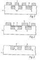
- Fig. 1 bis 4 sind Schnittansichten, die die einzelnen Herstellungsschritte einer Halbleiterstruktur, eingeschlossen eine Schottky-Diode, zeigen, und
- Fig. 5 zeigt den Grundriß einer Schottky-Diode nach Fig. 4.
- Die Schottky-Diode ist in einem Verbindungshalbleiter-Substrat ausgebildet, vorteilhafterweise : als Teil einer integrierten Schaltung. Zur Erläuterung wird lediglich die Herstellung einer Diode und eines daneben liegenden Transistors (MESFET) gezeigt.
- In den Fig. 1 bis 4 ist das Verbindungshalbleiter-Substrat 11 (Fig.1) mit der Maske 12 versehen und wird dann dem Strahl von Dotierionen hoher Energie zur Ausbildung einer vergrabenen n -leitenden Schicht aus den Zonen 13 und 13a ausgesetzt. Das Substrat besteht charakteristischerweise aus Galliumarsenid und das Dotiermittel aus Silicium, das aufgrund seiner großen Eindringtiefe bevorzugt wird. Mit doppelte geladenen Siliciumionen und einer Beschleunigungsspannung von 200 V, entsprechend einer Energie von 400 KeV, läßt sich eine Eindringtiefe von 0,5 bis 0,6 mm in dem Galliumarsenid-Substrat erzielen. Unter derartigen Bedingungen wurde gefunden, daß mit einer Dosis von 1014 Ionen/cm2 ein Dotierpegel von 1018 Siliciumatomen/cm3 erreicht werden kann, bei einer Oberflächenkonzentration von etwa 1017 Atome/cm3. Eine derartige Schicht kann durch einen Schottky-Kontakt vollständig ausgeräumt werden. In der Praxis erweist es sich als schwierig, Dotierpegel über 2 x 10¹⁸ Atome/cm3 zu erreichen.
- Als vergrabene Schicht ist die n -leitende Schicht von der Halbleiteroberfläche durch die schwach dotierte Oberflächenschicht 15 getrennt. Deren Stärke ist selbstverständlich eine Funktion der Implantationsenergie und beträgt 0,1 bis 0,2 µm.
- Nach der Implantation der vergrabenen Schicht 13 wird die Maske 12 entfernt und eine zweite Maske 14 (Fig. 2) aufgebracht. Eine Implantation von z.B. Silicium mit niedriger Energie (80 KeV, 4 x 10¹² Atome/cm3) bewirkt einen Anstieg des Dotierpegels der Oberflächenschicht 15 in den Bereichen 16, in denen ohmsche Kontakte auszubilden sind. Gleichzeitig legt der Dotiervorgang den Kanal des Feldeffekttransistors fest (schwach n-leitende Zone 17).
- Die Maske 14 wird entfernt und dieStmktur zur Aktivierung des implantierten Bereiches getempert. Man erhält die in Fig. 3 gezeigte Struktur mit zwei hochdotierten n+- leitenden Zonen 26, getrennt durch die schwach n-leitende Zone 17, sowie eine weitere n+-leitende Zone 29 mit einer schwach n-dotierten Oberflächenzone 20. Die ohmschen Kontakte 21, 22 und 23 (Fig. 4) werden danach an den n+-leitenden Zonen unter Ausbildung der entsprechenden ohmschen Kontakte der Schottky-Diode 41 und der Source- und Drain-Kontakt des MOS-Feldeffekttransistors 42 angebracht. Die Kontakte bestehen aus einer unteren Schicht 31 aus Gold/Germanium-Legierung und einer Oberschicht 32 aus Nickel.
- Die Schottky-Kontakte 24, 25 bestehen aus einer Schicht 33 aus Chrom und einer Oberschicht 34 aus Gold und sind an die schwach n-dotierten Zonen unter Ausbildung des entsprechenden Gate des MES-Feldeffekttransistors und der Schottky-Kontakte der Diode angebracht. Der Schottky-Kontakt 25 liegt auch über einen nichtimplantierten Bereich unter Ausbildung von Zwischenverbindungen und passiven Mikrowellenkomponenten wie Filter, Koppler und Übertragungslinien.
- Die Struktur der Schottky-Diode ist in Fig. 5 gezeigt. Man erkennt daß der ohmsche Kontakt 20 und der Schottky-Kontakt 25 nebeneinander auf dem Halbleitersubstrat angeordnet sind. Vorteilhafterweise sind die Kanten der Kontakte als ineinandergreifende Finger ausgebildet. Dies bewirkt ein Aufbrechen der Diodenstruktur in eine Vielzahl von parallel miteinander verbundenen kleineren Dioden, wodurch wesentlich die Parallelkapazität des Bauelements verringert wird. Die Diodenstruktur umfaßt charakteristischer Weise wenigstens 10 dieser kleineren Dioden, von denen jede eine Größe von ca. 1 x 2 µm aufweist. Da die vergrabene, den Strompfad durch die Diode bildende n -leitende Schicht eine relativ hohe Leitfähigkeit besitzt ist der Reihenwiderstand der Diode gering, so daß bei hohen Frequenzbereichen gearbeitet werden kann. Die vorhergehende Beschreibung betrifft die Herstellung einer Diodenstruktur als Teil einer integrierten Schaltung, man kann jedoch die Diode auch als diskretes Bauelement herstellen. Ebenso kann anstelle von GalLiumarsenid als bevorzugtes Material jeder andere beliebige Verbindungshalbleiter verwendet werden.
- In einem besonders vorteilhaften Ausführungsbeispiel der Erfindung ist das Substrat 11 mit einer dünnen, 3 x 10³ bis 5 x 10³ nm, vorzugsweise 4 x 10³ nm starken Oberflächenschicht aus Titan überzogen. Die Photolackmaske 12 ist dann auf dieser Schicht ausgebildet. Zweck der Titanschicht ist die Verhinderung jeder Verunreinigung, die aus dem Kontakt der Photomaske 12 mit der Halbleiteroberfläche resultieren könnte. Die Titanschicht wird durch Aufdampfen aufgebracht und wird nach der Implantationsstufe durch herkömmliches Naßätzen entfernt.
Claims (10)
1. Schottky-Diode ausgebildet in einem Verbindungshalbleiter-Substrat, gekennzeichnet durch eine. vergrabene Schicht (29) aus n-leitendem Material mit einer Oberflächenschicht (20) aus schwach n-dotiertem Material, wobei die Oberflächenschicht (20) mit einem Schottky-Kontakt (25) und die vergrabene Schicht mit einem ohmschen Kontakt (21) versehen ist.
2. Diodenstruktur nach Anspruch 1, gekennzeichnet durch eine Vielzahl von gleichartigen, parallel angeordneten, miteinander verbundenen Dioden.
3. Diodenstruktur nach Anspruch 1 oder 2, dadurch gekennzeichnet, daß die vergrabene Schicht (29) durch Implantation von Siliciumionen hergestellt ist.
4. Diodenstruktur nach Anspruch 3, dadurch gekennzeichnet, daß der Dotierpegel 1018 bis 2 x 10¹⁸ Atome/cm3 beträgt.
5. Integrierte Schaltung mit einem Schottky-Feldeffekttransistor und eine Schottky-Diodenstruktur, ausgebildet in einem Verbindungshalbleiter-Substrat, gekennzeichnet durch vergrabene n+-leitende, durch eine schwach n-dotierte Oberflächenschicht (17) getrennte Schichten (26) und eine vergrabene n -leitende Schicht (29) mit einer schwach n-dotierten Oberflächenschicht (20), wobei Schottky-Kontakte an den Oberflächenschichten angeordnet sind, und , daß erste, zweite und dritte ohmsche Kontakte (21, 22, 23) an den vergrabenen Schichten angebracht sind, die den ohmschen Kontakt der Diode (41) und die Source- und Drain-Kontakte des MES-Feldeffekttransistors (42) darstellen.
6. Integrierte Schaltung nach Anspruch 5, gekennzeichnet, durch mehrere Diodenstrukturen nach einem der Ansprüche 1 bis 4.
7. Verfahren zur Herstellung von Halbleiterstrukturen in einem Verbindungshalbleiter-Substrat, gekennzeichnet, durch die folgenden Verfahrensschritte:
- selektives Implantieren von Ionen hoher Energie in das Substrat unter Ausbildung einer vergrabenen n+-leitenden Schicht,
- Implantieren von Ionen geringerer Energie unter Ausbildung einer Oberflächenschicht aus schwach n-dotiertem Material,
- Anbringen eines Schottky-Kontaktes auf der Oberflächenschicht und eines ohmschen Kontaktes an der vergrabenen Schicht.
8. Verfahren nach Anspruch 7, dadurch gekennzeichnet, daß das Substrat aus Galliumarsenid besteht.
9. Verfahren nach den Ansprüchen 7 und 8, dadurch gekennzeichnet, daß die energiereichen Ionen doppelt geladene Siliciumionen sind, die bis zur Tiefe von 0,5 bis 0,6 µm implantiert werden.
10. Verfahren nach einem der Ansprüche 7 bis 8, dadurch gekennzeichnet, daß auf dem Halbleitersubstrat ein Titanfilm von 3 bis 5 x 103 µm und darauf eine Photolackschicht aufgebracht wird.
Applications Claiming Priority (4)
| Application Number | Priority Date | Filing Date | Title |
|---|---|---|---|
| GB8307145 | 1983-03-15 | ||
| GB8307145 | 1983-03-15 | ||
| GB08313853A GB2137412B (en) | 1983-03-15 | 1983-05-19 | Semiconductor device |
| GB8313853 | 1983-05-19 |
Publications (1)
| Publication Number | Publication Date |
|---|---|
| EP0123093A1 true EP0123093A1 (de) | 1984-10-31 |
Family
ID=26285521
Family Applications (1)
| Application Number | Title | Priority Date | Filing Date |
|---|---|---|---|
| EP84102643A Withdrawn EP0123093A1 (de) | 1983-03-15 | 1984-03-10 | Schottky-Diode, integrierte Schaltung mit Schottky-Diode und Verfahren zur Herstellung derselben |
Country Status (3)
| Country | Link |
|---|---|
| US (1) | US4745445A (de) |
| EP (1) | EP0123093A1 (de) |
| GB (1) | GB2137412B (de) |
Cited By (1)
| Publication number | Priority date | Publication date | Assignee | Title |
|---|---|---|---|---|
| EP0410911A1 (de) * | 1989-07-27 | 1991-01-30 | STMicroelectronics S.A. | Prozess zur Herstellung eines integrierten Leistungstransistor/Logik-Schaltkreises mit einer Diode. |
Families Citing this family (37)
| Publication number | Priority date | Publication date | Assignee | Title |
|---|---|---|---|---|
| FR2583221B1 (fr) * | 1985-06-07 | 1987-07-31 | Labo Electronique Physique | Dispositif semiconducteur pour la realisation des capacites de decouplage placees entre l'alimentation et la masse des circuits integres |
| US4811065A (en) * | 1987-06-11 | 1989-03-07 | Siliconix Incorporated | Power DMOS transistor with high speed body diode |
| US5014018A (en) * | 1987-10-06 | 1991-05-07 | Stanford University | Nonlinear transmission line for generation of picosecond electrical transients |
| US5352994A (en) * | 1987-10-06 | 1994-10-04 | The Board Of Trustees Of The Leland Stanford Junior University | Gallium arsenide monolithically integrated nonlinear transmission line impedance transformer |
| US5378939A (en) * | 1987-10-06 | 1995-01-03 | The Board Of Trustees Of The Leland Stanford Junior University | Gallium arsenide monolithically integrated sampling head using equivalent time sampling having a bandwidth greater than 100 Ghz |
| US5256996A (en) * | 1987-10-06 | 1993-10-26 | The Board Of Trustees Of The Leland Stanford, Junior University | Integrated coplanar strip nonlinear transmission line |
| US5347149A (en) * | 1989-11-29 | 1994-09-13 | Texas Instruments Incorporated | Integrated circuit and method |
| JP2003069046A (ja) * | 2001-08-30 | 2003-03-07 | Sanyo Electric Co Ltd | ショットキーバリアダイオードおよびその製造方法 |
| JP2003046094A (ja) * | 2001-07-27 | 2003-02-14 | Sanyo Electric Co Ltd | ショットキーバリアダイオードおよびその製造方法 |
| JP2003069047A (ja) * | 2001-08-30 | 2003-03-07 | Sanyo Electric Co Ltd | ショットキーバリアダイオードおよびその製造方法 |
| JP2003069048A (ja) * | 2001-08-30 | 2003-03-07 | Sanyo Electric Co Ltd | ショットキーバリアダイオードおよびその製造方法 |
| US7084716B2 (en) * | 2001-04-10 | 2006-08-01 | Picosecond Pulse Labs | Ultrafast sampler with coaxial transition |
| US6900710B2 (en) * | 2001-04-10 | 2005-05-31 | Picosecond Pulse Labs | Ultrafast sampler with non-parallel shockline |
| EP1280210A3 (de) * | 2001-07-27 | 2005-04-06 | Sanyo Electric Co., Ltd. | Schottkydiode und Verfahren zur Herstellung einer Schottkydiode |
| US20050179106A1 (en) * | 2001-07-27 | 2005-08-18 | Sanyo Electric Company, Ltd. | Schottky barrier diode |
| JP2003142697A (ja) * | 2001-10-31 | 2003-05-16 | Sanyo Electric Co Ltd | 集積型ショットキーバリアダイオードおよびその製造方法 |
| US7358834B1 (en) | 2002-08-29 | 2008-04-15 | Picosecond Pulse Labs | Transmission line voltage controlled nonlinear signal processors |
| EP1538673A4 (de) | 2002-09-09 | 2009-07-15 | Sanyo Electric Co | Schutzeinrichtung |
| JP4535668B2 (ja) * | 2002-09-09 | 2010-09-01 | 三洋電機株式会社 | 半導体装置 |
| JP4236442B2 (ja) * | 2002-10-17 | 2009-03-11 | 三洋電機株式会社 | スイッチ回路装置 |
| JP2004260139A (ja) * | 2003-02-06 | 2004-09-16 | Sanyo Electric Co Ltd | 半導体装置 |
| US7084475B2 (en) * | 2004-02-17 | 2006-08-01 | Velox Semiconductor Corporation | Lateral conduction Schottky diode with plural mesas |
| US7417266B1 (en) | 2004-06-10 | 2008-08-26 | Qspeed Semiconductor Inc. | MOSFET having a JFET embedded as a body diode |
| JP4939750B2 (ja) * | 2004-12-22 | 2012-05-30 | オンセミコンダクター・トレーディング・リミテッド | 化合物半導体スイッチ回路装置 |
| JP4939749B2 (ja) * | 2004-12-22 | 2012-05-30 | オンセミコンダクター・トレーディング・リミテッド | 化合物半導体スイッチ回路装置 |
| US7436039B2 (en) * | 2005-01-06 | 2008-10-14 | Velox Semiconductor Corporation | Gallium nitride semiconductor device |
| US8026568B2 (en) | 2005-11-15 | 2011-09-27 | Velox Semiconductor Corporation | Second Schottky contact metal layer to improve GaN Schottky diode performance |
| US7612629B2 (en) * | 2006-05-26 | 2009-11-03 | Picosecond Pulse Labs | Biased nonlinear transmission line comb generators |
| US7939853B2 (en) * | 2007-03-20 | 2011-05-10 | Power Integrations, Inc. | Termination and contact structures for a high voltage GaN-based heterojunction transistor |
| US9461153B2 (en) | 2011-11-16 | 2016-10-04 | Skyworks Solutions, Inc. | Devices and methods related to a barrier for metallization of a gallium based semiconductor |
| US9847407B2 (en) * | 2011-11-16 | 2017-12-19 | Skyworks Solutions, Inc. | Devices and methods related to a gallium arsenide Schottky diode having low turn-on voltage |
| US8633094B2 (en) | 2011-12-01 | 2014-01-21 | Power Integrations, Inc. | GaN high voltage HFET with passivation plus gate dielectric multilayer structure |
| US8940620B2 (en) | 2011-12-15 | 2015-01-27 | Power Integrations, Inc. | Composite wafer for fabrication of semiconductor devices |
| US8928037B2 (en) | 2013-02-28 | 2015-01-06 | Power Integrations, Inc. | Heterostructure power transistor with AlSiN passivation layer |
| US11749758B1 (en) | 2019-11-05 | 2023-09-05 | Semiq Incorporated | Silicon carbide junction barrier schottky diode with wave-shaped regions |
| US11469333B1 (en) | 2020-02-19 | 2022-10-11 | Semiq Incorporated | Counter-doped silicon carbide Schottky barrier diode |
| CN115360991A (zh) * | 2022-08-24 | 2022-11-18 | 中电国基南方集团有限公司 | 基于插指结构的限幅器芯片 |
Citations (4)
| Publication number | Priority date | Publication date | Assignee | Title |
|---|---|---|---|---|
| DE2543654B2 (de) * | 1975-09-30 | 1977-10-06 | Siemens AG, 1000 Berlin und 8000 München | Verfahren zur herstellung duenner leitender schichten zur realisierung von im normalzustand ausgeschalteten feldeffekttransistoren |
| EP0034729A2 (de) * | 1980-02-15 | 1981-09-02 | Siemens Aktiengesellschaft | Verfahren zur Herstellung einer GaAs-Halbleiteranordnung |
| US4301233A (en) * | 1980-05-29 | 1981-11-17 | Eaton Corporation | Beam lead Schottky barrier diode for operation at millimeter and submillimeter wave frequencies |
| EP0081423A1 (de) * | 1981-12-09 | 1983-06-15 | Thomson-Csf | Halbleiteranordnung mit niedriger parasitärer Kapazität mit "beam-lead" Typ Zuleitungen und Verfahren zur Herstellung dieser Anordnung |
Family Cites Families (15)
| Publication number | Priority date | Publication date | Assignee | Title |
|---|---|---|---|---|
| US3451912A (en) * | 1966-07-15 | 1969-06-24 | Ibm | Schottky-barrier diode formed by sputter-deposition processes |
| CH461646A (de) * | 1967-04-18 | 1968-08-31 | Ibm | Feld-Effekt-Transistor und Verfahren zu seiner Herstellung |
| GB1312678A (en) * | 1969-07-30 | 1973-04-04 | Gen Electric | Schottky barrier diode |
| IT1002232B (it) * | 1972-12-26 | 1976-05-20 | Gen Electric | Contatti a barriera schottky e metodi per fare i medesimi |
| US4212022A (en) * | 1973-04-30 | 1980-07-08 | Licentia Patent-Verwaltungs-G.M.B.H. | Field effect transistor with gate and drain electrodes on the side surface of a mesa |
| US3896473A (en) * | 1973-12-04 | 1975-07-22 | Bell Telephone Labor Inc | Gallium arsenide schottky barrier avalance diode array |
| JPS5318974A (en) * | 1976-08-05 | 1978-02-21 | Nec Corp | Semiconductor device for millimeter band mixer |
| GB1558506A (en) * | 1976-08-09 | 1980-01-03 | Mullard Ltd | Semiconductor devices having a rectifying metalto-semicondductor junction |
| US4238763A (en) * | 1977-08-10 | 1980-12-09 | National Research Development Corporation | Solid state microwave devices with small active contact and large passive contact |
| FR2471023A1 (fr) * | 1979-12-07 | 1981-06-12 | Ibm France | Reseau matriciel d'elements semi-conducteurs |
| US4338616A (en) * | 1980-02-19 | 1982-07-06 | Xerox Corporation | Self-aligned Schottky metal semi-conductor field effect transistor with buried source and drain |
| JPS56140667A (en) * | 1980-04-04 | 1981-11-04 | Nec Corp | Semiconductor device |
| US4463322A (en) * | 1981-08-14 | 1984-07-31 | Texas Instruments Incorporated | Self-biasing for FET-driven microwave VCOs |
| JPS5874084A (ja) * | 1981-10-29 | 1983-05-04 | Fujitsu Ltd | 半導体装置 |
| US4641174A (en) * | 1983-08-08 | 1987-02-03 | General Electric Company | Pinch rectifier |
-
1983
- 1983-05-19 GB GB08313853A patent/GB2137412B/en not_active Expired
-
1984
- 1984-03-10 EP EP84102643A patent/EP0123093A1/de not_active Withdrawn
-
1986
- 1986-12-22 US US06/945,244 patent/US4745445A/en not_active Expired - Lifetime
Patent Citations (4)
| Publication number | Priority date | Publication date | Assignee | Title |
|---|---|---|---|---|
| DE2543654B2 (de) * | 1975-09-30 | 1977-10-06 | Siemens AG, 1000 Berlin und 8000 München | Verfahren zur herstellung duenner leitender schichten zur realisierung von im normalzustand ausgeschalteten feldeffekttransistoren |
| EP0034729A2 (de) * | 1980-02-15 | 1981-09-02 | Siemens Aktiengesellschaft | Verfahren zur Herstellung einer GaAs-Halbleiteranordnung |
| US4301233A (en) * | 1980-05-29 | 1981-11-17 | Eaton Corporation | Beam lead Schottky barrier diode for operation at millimeter and submillimeter wave frequencies |
| EP0081423A1 (de) * | 1981-12-09 | 1983-06-15 | Thomson-Csf | Halbleiteranordnung mit niedriger parasitärer Kapazität mit "beam-lead" Typ Zuleitungen und Verfahren zur Herstellung dieser Anordnung |
Non-Patent Citations (3)
| Title |
|---|
| APPLIED PHYSICS LETTERS, Band 30, Nr. 7, 1. April 1977, New York, USA D.H. LEE et al. "Ion-implanted silicon profiles in GaAs" * |
| IEEE TRANSACTIONS ON ELECTRON DEVICES, Band ED-28, Nr. 2, Februar 1981, New York, USA J. CLIFTON et al. "High-performance quasi-optical GaAs monolithic mixer at 110 GHz", Seiten 155-157 * |
| RCA REVIEW, Band 42, Nr. 4, Dezember 1981, Princeton, USA L.C. UPADHYAYULA et al. "GaAs integrated circuit development for gigabit-rate signal processing", Seiten 522-541 * |
Cited By (3)
| Publication number | Priority date | Publication date | Assignee | Title |
|---|---|---|---|---|
| EP0410911A1 (de) * | 1989-07-27 | 1991-01-30 | STMicroelectronics S.A. | Prozess zur Herstellung eines integrierten Leistungstransistor/Logik-Schaltkreises mit einer Diode. |
| FR2650439A1 (fr) * | 1989-07-27 | 1991-02-01 | Sgs Thomson Microelectronics | Circuit integre vdmos/logique comprenant une diode |
| US5077586A (en) * | 1989-07-27 | 1991-12-31 | Sgs-Thomson Microelectronics S.A. | Vdmos/logic integrated circuit comprising a diode |
Also Published As
| Publication number | Publication date |
|---|---|
| GB2137412A (en) | 1984-10-03 |
| GB8313853D0 (en) | 1983-06-22 |
| GB2137412B (en) | 1987-03-04 |
| US4745445A (en) | 1988-05-17 |
Similar Documents
| Publication | Publication Date | Title |
|---|---|---|
| DE69032735T2 (de) | Verfahren zum Herstellen von Hochspannungs- und Niederspannungs-CMOS-Transistoren in einem einzigen integrierten Schaltungs-Chip | |
| DE69111929T2 (de) | Halbleiteranordnung auf einem dielektrischen isolierten Substrat. | |
| DE68926256T2 (de) | Komplementäre Halbleiteranordnung | |
| DE3110477C2 (de) | ||
| DE3856545T2 (de) | Halbleiterbauelement mit isoliertem Gatter | |
| DE2631873C2 (de) | Verfahren zur Herstellung eines Halbleiterbauelements mit einem Schottky-Kontakt auf einem zu einem anderen Bereich justierten Gatebereich und mit kleinem Serienwiderstand | |
| DE3881799T2 (de) | Verfahren zur Herstellung von CMOS-Bauelementen. | |
| DE2700873A1 (de) | Verfahren zur herstellung von komplementaeren isolierschicht-feldeffekttransistoren | |
| DE2728167A1 (de) | Verfahren zur vorbereitung eines siliziumsubstrats fuer die herstellung von mos-bauelementen | |
| DE3334337A1 (de) | Verfahren zur herstellung einer integrierten halbleitereinrichtung | |
| DE2718779A1 (de) | Mis-halbleiter-bauelement und verfahren zu dessen herstellung | |
| CH661150A5 (de) | Verfahren zum erzeugen einer schmalen nut in einem substratgebiet, insbesondere einem halbleitersubstratgebiet. | |
| DE2060333C3 (de) | Verfahren zur Herstellung einer Halbleiteranordnung mit einem Feldeffekttransistor mit isolierter Gateelektrode | |
| DE2404184A1 (de) | Mis-halbleitervorrichtung und verfahren zu deren herstellung | |
| EP0847593A1 (de) | Verfahren zur herstellung einer eeprom-halbleiterstruktur | |
| DE3709708A1 (de) | Feldeffekttransistor mit gering dotierter drainanordnung und verfahren zur herstellung desselben | |
| DE4139039C2 (de) | MOS-Halbleitervorrichtung | |
| DE3324332A1 (de) | Verfahren zur herstellung von cmos-transistoren auf einem siliziumsubstrat | |
| DE3329224C2 (de) | Verfahren zur Herstellung einer Bi-CMOS-Halbleiterschaltung | |
| DE4341516C2 (de) | Verfahren zum Herstellen eines Transistors | |
| EP0157926B1 (de) | Verfahren zum Herstellen einer hochintegrierten MOS-Feld-effekttransistorschaltung | |
| DE3424181A1 (de) | Cmos verfahren zur herstellung integrierter schaltungen, insbesondere dynamischer speicherzellen | |
| DE69023469T2 (de) | Integrierte Schaltung und Herstellungsverfahren dafür. | |
| DE102008039881A1 (de) | Graben-Transistor und Verfahren zur Herstellung desselben | |
| DE69026675T2 (de) | MIS-Kapazitätselement |
Legal Events
| Date | Code | Title | Description |
|---|---|---|---|
| PUAI | Public reference made under article 153(3) epc to a published international application that has entered the european phase |
Free format text: ORIGINAL CODE: 0009012 |
|
| AK | Designated contracting states |
Designated state(s): DE FR IT NL |
|
| 17P | Request for examination filed |
Effective date: 19841130 |
|
| RAP1 | Party data changed (applicant data changed or rights of an application transferred) |
Owner name: ITT INDUSTRIES INC. |
|
| STAA | Information on the status of an ep patent application or granted ep patent |
Free format text: STATUS: THE APPLICATION HAS BEEN WITHDRAWN |
|
| 18W | Application withdrawn |
Withdrawal date: 19870812 |
|
| RIN1 | Information on inventor provided before grant (corrected) |
Inventor name: MUN, JOSEPH Inventor name: BADAWI, MOHAMED HANI Inventor name: BARKER, GRAEME KENNETH |