EP0123128A2 - Sonde optoélectronique - Google Patents
Sonde optoélectronique Download PDFInfo
- Publication number
- EP0123128A2 EP0123128A2 EP84103018A EP84103018A EP0123128A2 EP 0123128 A2 EP0123128 A2 EP 0123128A2 EP 84103018 A EP84103018 A EP 84103018A EP 84103018 A EP84103018 A EP 84103018A EP 0123128 A2 EP0123128 A2 EP 0123128A2
- Authority
- EP
- European Patent Office
- Prior art keywords
- light
- marking
- scanning arrangement
- optoelectronic scanning
- arrangement according
- Prior art date
- Legal status (The legal status is an assumption and is not a legal conclusion. Google has not performed a legal analysis and makes no representation as to the accuracy of the status listed.)
- Granted
Links
Images

Classifications
-
- G—PHYSICS
- G06—COMPUTING OR CALCULATING; COUNTING
- G06K—GRAPHICAL DATA READING; PRESENTATION OF DATA; RECORD CARRIERS; HANDLING RECORD CARRIERS
- G06K7/00—Methods or arrangements for sensing record carriers, e.g. for reading patterns
- G06K7/10—Methods or arrangements for sensing record carriers, e.g. for reading patterns by electromagnetic radiation, e.g. optical sensing; by corpuscular radiation
- G06K7/10544—Methods or arrangements for sensing record carriers, e.g. for reading patterns by electromagnetic radiation, e.g. optical sensing; by corpuscular radiation by scanning of the records by radiation in the optical part of the electromagnetic spectrum
- G06K7/10821—Methods or arrangements for sensing record carriers, e.g. for reading patterns by electromagnetic radiation, e.g. optical sensing; by corpuscular radiation by scanning of the records by radiation in the optical part of the electromagnetic spectrum further details of bar or optical code scanning devices
- G06K7/10861—Methods or arrangements for sensing record carriers, e.g. for reading patterns by electromagnetic radiation, e.g. optical sensing; by corpuscular radiation by scanning of the records by radiation in the optical part of the electromagnetic spectrum further details of bar or optical code scanning devices sensing of data fields affixed to objects or articles, e.g. coded labels
-
- G—PHYSICS
- G11—INFORMATION STORAGE
- G11B—INFORMATION STORAGE BASED ON RELATIVE MOVEMENT BETWEEN RECORD CARRIER AND TRANSDUCER
- G11B15/00—Driving, starting or stopping record carriers of filamentary or web form; Driving both such record carriers and heads; Guiding such record carriers or containers therefor; Control thereof; Control of operating function
- G11B15/02—Control of operating function, e.g. switching from recording to reproducing
- G11B15/05—Control of operating function, e.g. switching from recording to reproducing by sensing features present on or derived from record carrier or container
- G11B15/06—Control of operating function, e.g. switching from recording to reproducing by sensing features present on or derived from record carrier or container by sensing auxiliary features on record carriers or containers, e.g. to stop machine near the end of a tape
- G11B15/08—Control of operating function, e.g. switching from recording to reproducing by sensing features present on or derived from record carrier or container by sensing auxiliary features on record carriers or containers, e.g. to stop machine near the end of a tape by photoelectric sensing
Definitions
- the invention relates to an optoelectronic scanning arrangement according to the preamble of patent claim 1.
- optoelectronic scanning arrangements for monitoring movement processes.
- the further explanations are limited to those optoelectronic scanning arrangements in which the light emitted by a light transmitter is reflected by a reflection surface and registered in a light receiver.
- the light transmitter and the light receiver are housed in one housing and form a so-called reflection light barrier.
- a first signal indicates that light reflected by the light receiver is registered, that is to say a reflective surface is present
- a second signal indicates that no reflected light is registered, that is to say no reflective surface is present.
- a mirrored surface as the reflecting surface and a surface made of light-absorbing material as the non-reflecting surface. It is also known to use a deep slit as the non-reflecting surface, which can also be lined with light-absorbing material. Stray light and contamination of the reflective surface reduce the difference between the two associated signals. A Contamination of the reflecting surface results in less light in the light receiver and therefore a smaller signal. Despite scanning the non-reflecting surface, scattered light gives more light in the light receiver and thus a larger signal. Furthermore, a dirty, non-reflecting surface also causes more light in the light receiver and thus a disturbance of the signal.
- the optoelectronic scanning arrangement according to the invention ensures reliable operation even when the two surfaces are contaminated.
- the non-reflecting surface is preferably inclined toward the hub of the flanged disc disc.
- the reflection light barrier L consists of a light transmitter LS and a light receiver. LE, which are housed together in one housing.
- a non-reflective marking NM is to be understood as an area through which no light emitted by the light transmitter LS is reflected into the light receiver LE.
- the reflective marking RM or the non-reflecting marking NM move relative to the light barrier L.
- the direction of movement is selected perpendicular to the plane of the drawing in FIGS. 1 to 3. 1 and 2, the axis light transmitter LS, light receiver LE is perpendicular to the direction of movement, in FIG. 3 the axis light transmitter LS, light receiver LE is arranged parallel to the direction of movement.
- the light barrier L is arranged at a distance A from the reflective marking RM, which is determined by the geometric design of the light barrier L, since the light emitted by the light transmitter LS (represented by arrows in FIGS. 1 to 3) provided), while observing the angle of reflection from the reflective marking RM is reflected into the light receiver LE.
- the surface of the reflective marking RM is mirrored, for example, in order to increase the degree of reflection.
- the non-reflecting marking NM (FIGS. 2 and 3) is a surface which is inclined by an angle W against the axis of the light beam emitted by the light transmitter LS.
- the angle W is chosen so that, despite the divergence of the light beams, no light coming from the light transmitter LS is reflected by the non-reflective marking NM into the light receiver LE.
- This area can also be mirrored.
- the optoelectronic scanning arrangement according to the invention can be used, for example, to monitor the rotation of a tape reel, in particular the fixed winding in a magnetic tape device.
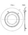
- the fixed winding consists of a hub N and two flanges, the opaque device facing the device being designed.
- the rear side is shown in plan view in FIG. 4, and such an opaque flanged washer B is shown in section in FIG. 5.
- Radial are the reflective marking RM on one half of the flanged wheel B and the non-reflective marking on the other half. tion NM arranged.
- the scanning reflection light barrier L is shown in FIG. 5.
- the surface of the non-reflective marking NM ' is inclined towards the hub N, so that the optoelectronic scanning arrangement is insensitive to external light entering from outside.
- the non-reflecting marking NM forms, on average (FIG. 5), a triangular profile together with the flanged wheel B.
- the height of this profile can be smaller, the smaller the divergence of the light sender LS emitted light, and the closer the photoelectric reflex switch L can be attached to the flanged wheel B.
Landscapes
- Physics & Mathematics (AREA)
- Electromagnetism (AREA)
- Engineering & Computer Science (AREA)
- Health & Medical Sciences (AREA)
- General Health & Medical Sciences (AREA)
- Toxicology (AREA)
- Artificial Intelligence (AREA)
- Computer Vision & Pattern Recognition (AREA)
- General Physics & Mathematics (AREA)
- Theoretical Computer Science (AREA)
- Optical Transform (AREA)
- Length Measuring Devices By Optical Means (AREA)
Applications Claiming Priority (2)
| Application Number | Priority Date | Filing Date | Title |
|---|---|---|---|
| DE3310394 | 1983-03-22 | ||
| DE3310394A DE3310394C1 (de) | 1983-03-22 | 1983-03-22 | Optoelektronische Abtastanordnung |
Publications (3)
| Publication Number | Publication Date |
|---|---|
| EP0123128A2 true EP0123128A2 (fr) | 1984-10-31 |
| EP0123128A3 EP0123128A3 (en) | 1986-03-12 |
| EP0123128B1 EP0123128B1 (fr) | 1989-11-15 |
Family
ID=6194309
Family Applications (1)
| Application Number | Title | Priority Date | Filing Date |
|---|---|---|---|
| EP84103018A Expired EP0123128B1 (fr) | 1983-03-22 | 1984-03-19 | Sonde optoélectronique |
Country Status (3)
| Country | Link |
|---|---|
| US (1) | US4673809A (fr) |
| EP (1) | EP0123128B1 (fr) |
| DE (2) | DE3310394C1 (fr) |
Cited By (2)
| Publication number | Priority date | Publication date | Assignee | Title |
|---|---|---|---|---|
| WO1995019012A1 (fr) * | 1994-01-11 | 1995-07-13 | Hine Design Incorporated | Appareil et procedes permettant d'inspecter des marques d'identification sur des tranches de semiconducteur |
| DE102017001463A1 (de) * | 2017-02-15 | 2018-08-16 | Minebea Mitsumi Inc. | Spindelmotor |
Families Citing this family (6)
| Publication number | Priority date | Publication date | Assignee | Title |
|---|---|---|---|---|
| US4780610A (en) * | 1986-03-04 | 1988-10-25 | Alps Electric Co., Ltd. | Optical rotary encoder having superposed metal plate and shield plate |
| US4811002A (en) * | 1986-10-03 | 1989-03-07 | Honda Giken Kogyo Kabushiki Kaisha | Relative positional relation detecting system |
| US5616908A (en) * | 1991-09-17 | 1997-04-01 | Metrologic Instruments, Inc. | Automatic countertop laser scanner with flickering laser scanner beam for improved visibility thereof during bar code symbol reading |
| US5388048A (en) * | 1993-02-16 | 1995-02-07 | Silicon Heights Limited | Vehicle anti-collison device |
| JPH11201779A (ja) * | 1998-01-07 | 1999-07-30 | Fanuc Ltd | 光学式エンコーダ |
| US20030156531A1 (en) * | 2002-02-19 | 2003-08-21 | G6 Science Corporation | Disk data storage media with edge track data surface, methods to manufacture, exploit and convert conventional disk media to that having an edge track data surface |
Family Cites Families (9)
| Publication number | Priority date | Publication date | Assignee | Title |
|---|---|---|---|---|
| DE760288C (de) * | 1940-10-19 | 1954-04-22 | Aeg | Anordnung zur Messung und Anzeige der Frequenz von periodischen Vorgaengen, insbesondere zur leistungslosen Fernanzeige von Drehzahlen |
| DE2135195C3 (de) * | 1971-07-14 | 1974-05-09 | Magyar Optikai Muevek | Unter Verwendung von Abbildungselementen optisch abtastbare, informationstragende Einrichtung an bewegten Fahrzeugen |
| GB1416679A (en) * | 1971-11-05 | 1975-12-03 | Ferraris Dev Eng Co Ltd | Measurement of rotation of a rotary member |
| US4175236A (en) * | 1977-12-23 | 1979-11-20 | Owens-Illinois, Inc. | Method and apparatus of cavity identification of mold of origin |
| DE2909735B2 (de) * | 1979-03-13 | 1981-01-15 | Becker Autoradiowerk Gmbh, 7516 Karlsbad | Optischer Impulsgeber |
| US4387299A (en) * | 1979-06-25 | 1983-06-07 | Yazaki Sogyo Kabushiki Kaisha | Travel-distance signal generator for vehicles |
| US4409469A (en) * | 1980-01-21 | 1983-10-11 | Sharp Kabushiki Kaisha | Optical bar code reader |
| US4547073A (en) * | 1981-02-17 | 1985-10-15 | Matsushita Electric Industrial Co., Ltd. | Surface examining apparatus and method |
| US4536650A (en) * | 1983-01-26 | 1985-08-20 | Ing. C. Olivetti & C., S.P.A. | Optical transducer with a transparent shutter disk |
-
1983
- 1983-03-22 DE DE3310394A patent/DE3310394C1/de not_active Expired
-
1984
- 1984-03-19 EP EP84103018A patent/EP0123128B1/fr not_active Expired
- 1984-03-19 DE DE8484103018T patent/DE3480495D1/de not_active Expired
-
1986
- 1986-08-18 US US06/899,184 patent/US4673809A/en not_active Expired - Fee Related
Cited By (3)
| Publication number | Priority date | Publication date | Assignee | Title |
|---|---|---|---|---|
| WO1995019012A1 (fr) * | 1994-01-11 | 1995-07-13 | Hine Design Incorporated | Appareil et procedes permettant d'inspecter des marques d'identification sur des tranches de semiconducteur |
| US5831738A (en) * | 1994-01-11 | 1998-11-03 | Hine Design Inc. | Apparatus and methods for viewing identification marks on semiconductor wafers |
| DE102017001463A1 (de) * | 2017-02-15 | 2018-08-16 | Minebea Mitsumi Inc. | Spindelmotor |
Also Published As
| Publication number | Publication date |
|---|---|
| DE3310394C1 (de) | 1984-08-16 |
| EP0123128A3 (en) | 1986-03-12 |
| EP0123128B1 (fr) | 1989-11-15 |
| DE3480495D1 (de) | 1989-12-21 |
| US4673809A (en) | 1987-06-16 |
Similar Documents
| Publication | Publication Date | Title |
|---|---|---|
| DE3517889C2 (fr) | ||
| EP0897120B1 (fr) | Dispositif pour localiser l'entrée d'objets dans un domaine spatial surveillé | |
| DE3926228C2 (fr) | ||
| DE9219146U1 (de) | Lichtelektrische Vorrichtung zum Orten von Hindernissen | |
| EP0377097A1 (fr) | Capteur de l'angle de direction pour un véhicule automobile | |
| EP2063230B1 (fr) | Dispositif optique de mesure de la position | |
| DE69001657T2 (de) | Optische kodierer. | |
| DE202011001702U1 (de) | Detektor und mobiler Automat mit demselben | |
| EP0123929A2 (fr) | Dispositif pour la détection de défauts | |
| EP0123128A2 (fr) | Sonde optoélectronique | |
| EP0557564A1 (fr) | Dispositif de montage pour un dispositif pour mesurer des angles | |
| DE19830120B4 (de) | Optoelektronische Sensoreinrichtung | |
| DE1774562B2 (de) | Anordnung zum Abtasten von rückstrahlenden Markierungen | |
| DE102016114477A1 (de) | Fördervorrichtung | |
| DE69123899T2 (de) | Optisches Gerät zum Detektieren der Position | |
| DE69205062T2 (de) | Optische Abtastvorrichtung. | |
| DE2459358B2 (de) | Vorrichtung zur erfassung einer reflektierenden flaeche auf einem traegerkoerper | |
| DE112016003886T5 (de) | Flüssigkeitssensor | |
| DE2236482A1 (de) | Unfallschutzlichtvorhang | |
| DE3710068C2 (fr) | ||
| DE10147176A1 (de) | Sensoreinrichtung zur Erfassung der Benetzung einer Scheibe, insbesondere einer Kraftfahrzeugscheibe | |
| DE2124444A1 (de) | Verfahren zum Bestimmen der Dicke oder Breite von Werkstücken | |
| DE19946220C1 (de) | Optoelektronische Sensoreinrichtung | |
| DE19838731C2 (de) | Lenkwinkelsensor | |
| DE69219005T2 (de) | Optischer Kopfantrieb |
Legal Events
| Date | Code | Title | Description |
|---|---|---|---|
| PUAI | Public reference made under article 153(3) epc to a published international application that has entered the european phase |
Free format text: ORIGINAL CODE: 0009012 |
|
| AK | Designated contracting states |
Designated state(s): DE FR GB |
|
| 17P | Request for examination filed |
Effective date: 19841221 |
|
| PUAL | Search report despatched |
Free format text: ORIGINAL CODE: 0009013 |
|
| AK | Designated contracting states |
Kind code of ref document: A3 Designated state(s): DE FR GB |
|
| 17Q | First examination report despatched |
Effective date: 19880205 |
|
| GRAA | (expected) grant |
Free format text: ORIGINAL CODE: 0009210 |
|
| AK | Designated contracting states |
Kind code of ref document: B1 Designated state(s): DE FR GB |
|
| REF | Corresponds to: |
Ref document number: 3480495 Country of ref document: DE Date of ref document: 19891221 |
|
| ET | Fr: translation filed | ||
| GBT | Gb: translation of ep patent filed (gb section 77(6)(a)/1977) | ||
| PGFP | Annual fee paid to national office [announced via postgrant information from national office to epo] |
Ref country code: FR Payment date: 19900321 Year of fee payment: 7 |
|
| PGFP | Annual fee paid to national office [announced via postgrant information from national office to epo] |
Ref country code: DE Payment date: 19900528 Year of fee payment: 7 |
|
| PLBE | No opposition filed within time limit |
Free format text: ORIGINAL CODE: 0009261 |
|
| STAA | Information on the status of an ep patent application or granted ep patent |
Free format text: STATUS: NO OPPOSITION FILED WITHIN TIME LIMIT |
|
| 26N | No opposition filed | ||
| PGFP | Annual fee paid to national office [announced via postgrant information from national office to epo] |
Ref country code: GB Payment date: 19910218 Year of fee payment: 8 |
|
| PG25 | Lapsed in a contracting state [announced via postgrant information from national office to epo] |
Ref country code: FR Effective date: 19911129 |
|
| PG25 | Lapsed in a contracting state [announced via postgrant information from national office to epo] |
Ref country code: DE Effective date: 19920101 |
|
| REG | Reference to a national code |
Ref country code: FR Ref legal event code: ST |
|
| PG25 | Lapsed in a contracting state [announced via postgrant information from national office to epo] |
Ref country code: GB Effective date: 19920319 |
|
| GBPC | Gb: european patent ceased through non-payment of renewal fee |