EP0124261B1 - Procédé de fabrication d'un couche monocristalline sur un isolant - Google Patents
Procédé de fabrication d'un couche monocristalline sur un isolant Download PDFInfo
- Publication number
- EP0124261B1 EP0124261B1 EP84302118A EP84302118A EP0124261B1 EP 0124261 B1 EP0124261 B1 EP 0124261B1 EP 84302118 A EP84302118 A EP 84302118A EP 84302118 A EP84302118 A EP 84302118A EP 0124261 B1 EP0124261 B1 EP 0124261B1
- Authority
- EP
- European Patent Office
- Prior art keywords
- layer
- nonmonocrystalline
- sources
- rod
- region
- Prior art date
- Legal status (The legal status is an assumption and is not a legal conclusion. Google has not performed a legal analysis and makes no representation as to the accuracy of the status listed.)
- Expired
Links
Images


Classifications
-
- H—ELECTRICITY
- H10—SEMICONDUCTOR DEVICES; ELECTRIC SOLID-STATE DEVICES NOT OTHERWISE PROVIDED FOR
- H10P—GENERIC PROCESSES OR APPARATUS FOR THE MANUFACTURE OR TREATMENT OF DEVICES COVERED BY CLASS H10
- H10P14/00—Formation of materials, e.g. in the shape of layers or pillars
- H10P14/20—Formation of materials, e.g. in the shape of layers or pillars of semiconductor materials
- H10P14/38—Formation of materials, e.g. in the shape of layers or pillars of semiconductor materials characterised by treatments done after the formation of the materials
- H10P14/3802—Crystallisation or recrystallisation of non-monocrystalline semiconductor materials, e.g. regrowth
-
- C—CHEMISTRY; METALLURGY
- C30—CRYSTAL GROWTH
- C30B—SINGLE-CRYSTAL GROWTH; UNIDIRECTIONAL SOLIDIFICATION OF EUTECTIC MATERIAL OR UNIDIRECTIONAL DEMIXING OF EUTECTOID MATERIAL; REFINING BY ZONE-MELTING OF MATERIAL; PRODUCTION OF A HOMOGENEOUS POLYCRYSTALLINE MATERIAL WITH DEFINED STRUCTURE; SINGLE CRYSTALS OR HOMOGENEOUS POLYCRYSTALLINE MATERIAL WITH DEFINED STRUCTURE; AFTER-TREATMENT OF SINGLE CRYSTALS OR A HOMOGENEOUS POLYCRYSTALLINE MATERIAL WITH DEFINED STRUCTURE; APPARATUS THEREFOR
- C30B13/00—Single-crystal growth by zone-melting; Refining by zone-melting
-
- C—CHEMISTRY; METALLURGY
- C30—CRYSTAL GROWTH
- C30B—SINGLE-CRYSTAL GROWTH; UNIDIRECTIONAL SOLIDIFICATION OF EUTECTIC MATERIAL OR UNIDIRECTIONAL DEMIXING OF EUTECTOID MATERIAL; REFINING BY ZONE-MELTING OF MATERIAL; PRODUCTION OF A HOMOGENEOUS POLYCRYSTALLINE MATERIAL WITH DEFINED STRUCTURE; SINGLE CRYSTALS OR HOMOGENEOUS POLYCRYSTALLINE MATERIAL WITH DEFINED STRUCTURE; AFTER-TREATMENT OF SINGLE CRYSTALS OR A HOMOGENEOUS POLYCRYSTALLINE MATERIAL WITH DEFINED STRUCTURE; APPARATUS THEREFOR
- C30B13/00—Single-crystal growth by zone-melting; Refining by zone-melting
- C30B13/16—Heating of the molten zone
- C30B13/22—Heating of the molten zone by irradiation or electric discharge
- C30B13/24—Heating of the molten zone by irradiation or electric discharge using electromagnetic waves
-
- C—CHEMISTRY; METALLURGY
- C30—CRYSTAL GROWTH
- C30B—SINGLE-CRYSTAL GROWTH; UNIDIRECTIONAL SOLIDIFICATION OF EUTECTIC MATERIAL OR UNIDIRECTIONAL DEMIXING OF EUTECTOID MATERIAL; REFINING BY ZONE-MELTING OF MATERIAL; PRODUCTION OF A HOMOGENEOUS POLYCRYSTALLINE MATERIAL WITH DEFINED STRUCTURE; SINGLE CRYSTALS OR HOMOGENEOUS POLYCRYSTALLINE MATERIAL WITH DEFINED STRUCTURE; AFTER-TREATMENT OF SINGLE CRYSTALS OR A HOMOGENEOUS POLYCRYSTALLINE MATERIAL WITH DEFINED STRUCTURE; APPARATUS THEREFOR
- C30B29/00—Single crystals or homogeneous polycrystalline material with defined structure characterised by the material or by their shape
- C30B29/60—Single crystals or homogeneous polycrystalline material with defined structure characterised by the material or by their shape characterised by shape
-
- H—ELECTRICITY
- H10—SEMICONDUCTOR DEVICES; ELECTRIC SOLID-STATE DEVICES NOT OTHERWISE PROVIDED FOR
- H10P—GENERIC PROCESSES OR APPARATUS FOR THE MANUFACTURE OR TREATMENT OF DEVICES COVERED BY CLASS H10
- H10P14/00—Formation of materials, e.g. in the shape of layers or pillars
- H10P14/20—Formation of materials, e.g. in the shape of layers or pillars of semiconductor materials
- H10P14/29—Formation of materials, e.g. in the shape of layers or pillars of semiconductor materials characterised by the substrates
- H10P14/2901—Materials
- H10P14/2902—Materials being Group IVA materials
- H10P14/2905—Silicon, silicon germanium or germanium
-
- H—ELECTRICITY
- H10—SEMICONDUCTOR DEVICES; ELECTRIC SOLID-STATE DEVICES NOT OTHERWISE PROVIDED FOR
- H10P—GENERIC PROCESSES OR APPARATUS FOR THE MANUFACTURE OR TREATMENT OF DEVICES COVERED BY CLASS H10
- H10P14/00—Formation of materials, e.g. in the shape of layers or pillars
- H10P14/20—Formation of materials, e.g. in the shape of layers or pillars of semiconductor materials
- H10P14/29—Formation of materials, e.g. in the shape of layers or pillars of semiconductor materials characterised by the substrates
- H10P14/2926—Crystal orientations
-
- H—ELECTRICITY
- H10—SEMICONDUCTOR DEVICES; ELECTRIC SOLID-STATE DEVICES NOT OTHERWISE PROVIDED FOR
- H10P—GENERIC PROCESSES OR APPARATUS FOR THE MANUFACTURE OR TREATMENT OF DEVICES COVERED BY CLASS H10
- H10P14/00—Formation of materials, e.g. in the shape of layers or pillars
- H10P14/20—Formation of materials, e.g. in the shape of layers or pillars of semiconductor materials
- H10P14/32—Formation of materials, e.g. in the shape of layers or pillars of semiconductor materials characterised by intermediate layers between substrates and deposited layers
- H10P14/3202—Materials thereof
- H10P14/3238—Materials thereof being insulating materials
-
- H—ELECTRICITY
- H10—SEMICONDUCTOR DEVICES; ELECTRIC SOLID-STATE DEVICES NOT OTHERWISE PROVIDED FOR
- H10P—GENERIC PROCESSES OR APPARATUS FOR THE MANUFACTURE OR TREATMENT OF DEVICES COVERED BY CLASS H10
- H10P14/00—Formation of materials, e.g. in the shape of layers or pillars
- H10P14/20—Formation of materials, e.g. in the shape of layers or pillars of semiconductor materials
- H10P14/32—Formation of materials, e.g. in the shape of layers or pillars of semiconductor materials characterised by intermediate layers between substrates and deposited layers
- H10P14/3242—Structure
- H10P14/3244—Layer structure
- H10P14/3251—Layer structure consisting of three or more layers
-
- H—ELECTRICITY
- H10—SEMICONDUCTOR DEVICES; ELECTRIC SOLID-STATE DEVICES NOT OTHERWISE PROVIDED FOR
- H10P—GENERIC PROCESSES OR APPARATUS FOR THE MANUFACTURE OR TREATMENT OF DEVICES COVERED BY CLASS H10
- H10P14/00—Formation of materials, e.g. in the shape of layers or pillars
- H10P14/20—Formation of materials, e.g. in the shape of layers or pillars of semiconductor materials
- H10P14/34—Deposited materials, e.g. layers
- H10P14/3402—Deposited materials, e.g. layers characterised by the chemical composition
- H10P14/3404—Deposited materials, e.g. layers characterised by the chemical composition being Group IVA materials
- H10P14/3411—Silicon, silicon germanium or germanium
-
- H—ELECTRICITY
- H10—SEMICONDUCTOR DEVICES; ELECTRIC SOLID-STATE DEVICES NOT OTHERWISE PROVIDED FOR
- H10P—GENERIC PROCESSES OR APPARATUS FOR THE MANUFACTURE OR TREATMENT OF DEVICES COVERED BY CLASS H10
- H10P14/00—Formation of materials, e.g. in the shape of layers or pillars
- H10P14/20—Formation of materials, e.g. in the shape of layers or pillars of semiconductor materials
- H10P14/34—Deposited materials, e.g. layers
- H10P14/3451—Structure
- H10P14/3452—Microstructure
- H10P14/3458—Monocrystalline
-
- H—ELECTRICITY
- H10—SEMICONDUCTOR DEVICES; ELECTRIC SOLID-STATE DEVICES NOT OTHERWISE PROVIDED FOR
- H10P—GENERIC PROCESSES OR APPARATUS FOR THE MANUFACTURE OR TREATMENT OF DEVICES COVERED BY CLASS H10
- H10P14/00—Formation of materials, e.g. in the shape of layers or pillars
- H10P14/20—Formation of materials, e.g. in the shape of layers or pillars of semiconductor materials
- H10P14/38—Formation of materials, e.g. in the shape of layers or pillars of semiconductor materials characterised by treatments done after the formation of the materials
- H10P14/3802—Crystallisation or recrystallisation of non-monocrystalline semiconductor materials, e.g. regrowth
- H10P14/382—Scanning of a beam
-
- H—ELECTRICITY
- H10—SEMICONDUCTOR DEVICES; ELECTRIC SOLID-STATE DEVICES NOT OTHERWISE PROVIDED FOR
- H10P—GENERIC PROCESSES OR APPARATUS FOR THE MANUFACTURE OR TREATMENT OF DEVICES COVERED BY CLASS H10
- H10P34/00—Irradiation with electromagnetic or particle radiation of wafers, substrates or parts of devices
- H10P34/40—Irradiation with electromagnetic or particle radiation of wafers, substrates or parts of devices with high-energy radiation
- H10P34/42—Irradiation with electromagnetic or particle radiation of wafers, substrates or parts of devices with high-energy radiation with electromagnetic radiation, e.g. laser annealing
- H10P34/422—Irradiation with electromagnetic or particle radiation of wafers, substrates or parts of devices with high-energy radiation with electromagnetic radiation, e.g. laser annealing using incoherent radiation
-
- H—ELECTRICITY
- H10—SEMICONDUCTOR DEVICES; ELECTRIC SOLID-STATE DEVICES NOT OTHERWISE PROVIDED FOR
- H10P—GENERIC PROCESSES OR APPARATUS FOR THE MANUFACTURE OR TREATMENT OF DEVICES COVERED BY CLASS H10
- H10P95/00—Generic processes or apparatus for manufacture or treatments not covered by the other groups of this subclass
- H10P95/90—Thermal treatments, e.g. annealing or sintering
-
- Y—GENERAL TAGGING OF NEW TECHNOLOGICAL DEVELOPMENTS; GENERAL TAGGING OF CROSS-SECTIONAL TECHNOLOGIES SPANNING OVER SEVERAL SECTIONS OF THE IPC; TECHNICAL SUBJECTS COVERED BY FORMER USPC CROSS-REFERENCE ART COLLECTIONS [XRACs] AND DIGESTS
- Y10—TECHNICAL SUBJECTS COVERED BY FORMER USPC
- Y10T—TECHNICAL SUBJECTS COVERED BY FORMER US CLASSIFICATION
- Y10T117/00—Single-crystal, oriented-crystal, and epitaxy growth processes; non-coating apparatus therefor
- Y10T117/10—Apparatus
- Y10T117/1024—Apparatus for crystallization from liquid or supercritical state
- Y10T117/1076—Apparatus for crystallization from liquid or supercritical state having means for producing a moving solid-liquid-solid zone
- Y10T117/108—Including a solid member other than seed or product contacting the liquid [e.g., crucible, immersed heating element]
-
- Y—GENERAL TAGGING OF NEW TECHNOLOGICAL DEVELOPMENTS; GENERAL TAGGING OF CROSS-SECTIONAL TECHNOLOGIES SPANNING OVER SEVERAL SECTIONS OF THE IPC; TECHNICAL SUBJECTS COVERED BY FORMER USPC CROSS-REFERENCE ART COLLECTIONS [XRACs] AND DIGESTS
- Y10—TECHNICAL SUBJECTS COVERED BY FORMER USPC
- Y10T—TECHNICAL SUBJECTS COVERED BY FORMER US CLASSIFICATION
- Y10T117/00—Single-crystal, oriented-crystal, and epitaxy growth processes; non-coating apparatus therefor
- Y10T117/10—Apparatus
- Y10T117/1024—Apparatus for crystallization from liquid or supercritical state
- Y10T117/1076—Apparatus for crystallization from liquid or supercritical state having means for producing a moving solid-liquid-solid zone
- Y10T117/1088—Apparatus for crystallization from liquid or supercritical state having means for producing a moving solid-liquid-solid zone including heating or cooling details
Definitions
- the present invention relates to a process for producing a monocrystalline layer on an insulator.
- a silicon wafer for such use generally accommodates three-dimensional LSI's in the bulk of the wafer.
- the silicon wafer is mounted on a carbon plate heater to heat the entire bulk of the wafer by conduction to about 1,200°C.
- a carbon strip heater moves over the silicon wafer to anneal by heat radiation a local region of the wafer at about 1,420°C, the melting point of silicon.
- the beam of heat from the carbon strip heater melts the local region so as to transform the polycrystalline silicon to monocrystalline silicon.
- Semiconductor elements can then be formed on the silicon monocrystalline layer.
- the overall heating and local annealing of the wafer are conducted in an inert atmosphere so as to reduce oxidation and evaporation of the carbon.
- S. Iwamatsu disclosed, in Japanese Unexamined Patent Publication (Kokai) No. 56-80138, using a rod-like heat source, such as a xenon lamp provided with a reflective mirror, to scan an energy beam having a linear section over a semiconductor wafer or a layer deposited thereon. From our experience, however, it is substantially impossible for a single commercially available lamp to melt a portion of a semiconductor wafer and transform a non-monocrystalline layer of silicon to a monocrystalline layer, due to its low emitting power, even if the beam is focused thereon.
- a rod-like heat source such as a xenon lamp provided with a reflective mirror
- M. Haond et al disclose, in Electronics Letters, August 19, 1982, vol. 18, No. 17, using a plurality of low-power halogen lamps to preheat a wafer from the back side to a temperature of 300°C to 1100°C and using a beam focused on the front surface to supply the additional amount of energy necessary to reach a temperature from 1,000°C to the melting point of silicon on certain spot, typically 1 cm in diameter.
- This annealing is carried out in ambient air while the sample is moved along a spiral at a constant speed.
- the wafer is still heated as a whole from the back side by the plurality of lamps, which leads to rediffusion of a previously implanted impurity.
- EP-A-0 106 722 describes a state of the art according to Art.54(3) concerning a process for producing a monocrystalline layer on an insulator, particularly in a wafer adapted for use in producing large-scale integrated circuits, comprising the steps of:
- a process for producing a monocrystalline layer on an insulator comprising the steps of:
- An embodiment of the present invention can provide a process for producing a monocrystalline layer by locally annealing for a short time to a nonmonocrystalline layer formed on an insulator in a semiconductor wafer.
- An embodiment of the present invention can provide a process for producing a monocrystalline layer on an insulator with reduced thermal strain in the monocrystalline layer.
- An embodiment of the present invention can provide a process for producing a monocrystalline layer on an insulator provided in a semiconductor wafer with reduced rediffusion of the previously implanted impurity.
- FIG. 1 A silicon wafer 1 is mounted on a carbon plate heater 2.
- a carbon strip heater 3 moves over the silicon wafer 1.
- the carbon plate heater 2 heats the bulk of the silicon wafer 1 overall by conduction, while the carbon strip heater 3 anneals by heat radiation a local region of the silicon wafer 1.
- the beam of heat from the carbon strip heater 3 melts the local region so as to transform the polycrystalline silicon to monocrystalline silicon.
- FIG. 2 is a schematic view of an embodiment according to the present invention.
- a silicon wafer 1 is covered with an oxide layer 4 and a polycrystalline silicon layer 5.
- the wafer 1 moves in the direction A relative to lamps 6a, 6b located at opposite sides thereof.
- the first lamp 6a is located at the front of an oxide cap layer 7 and is provided with an elliptical semicylindrical reflective mirror 8a forfocusing the beam of heat-producing radiation at a region 5ab to be melted.
- the second lamp 6b provided with an elliptical semicylindrical reflective mirror 8b, is located at the back of the bulk of the silicon wafer 1.
- the lamps are rod-like lamps, such as halogen or inert-gas filled tungsten lamps or mercury discharge lamps.
- rod-like carbon heaters may be used, without mirrors.
- the beams of radiation from the two lamps are focused on the same region 5ab.
- the second lamp 6b may have less power than the first lamp 6a.
- a similar silicon wafer 1 is irradiated with beams of heat-producing radiation emitted from two lamps 9a, 9b, both located at the front of the silicon wafer 1
- a single elliptical semicylindrical reflective mirror 10 is provided for the two lamps 9a, 9b, thus reducing the size and simplifying the structure of the heat sources.
- the lamp 9a heats a narrow region 5a, while the lamp 9b heats a broader region 5b. This also reduces the thermal strain.
- a semiconductor wafer sample as shown in Fig. 4.
- the sample comprised a crystal surface (100) p-type silicon wafer 1 of 400 Il m thickness having an As ion-implanted layer 1a and sequentially thereon a Si 3 N 4 layer 4a, a phosphosilicate glass (PSG) insulator layer 4b, another Si 3 N 4 layer 4c, a polycrystalline silicon layer 5 of 0.4 pm thickness, and a thick PSG cap layer 7.
- PSG phosphosilicate glass
- the sample was inserted between two halogen- filled tungsten lamps as shown in Fig. 2.
- the two lamps 6a, 6b heated the sample with beams of radiation focused at region 5ab.
- the front and back beams had a thermal density of 500 W/cm 2 and 100 W/cm 2 , respectively.
- the relative speed of movement of the sample to the beams was 5.4 cm/min.
- the polycrystalline silicon layer 5 was melted and transformed to a monocrystalline 5c.
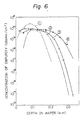
- Figure 6 shows the impurity profile of semiconductor wafers, i.e., the relationship between the depth of the semiconductor wafer and the concentration of the impurity.
- Curve 1 shows the profile of As ion impurity implanted with a dose rate of 2 x 10 15 /cm 2 at 150 keV.
- Curve 2 shows the profile immediately after growing the layers 4a, 4b, 4c, 5, and 7, shown in Fig. 4.
- Curve 3 shows the profile after annealing the layer 5 so as to form a monocrystalline silicon layer according to the present invention.
- Curve 4 is comparative and shows the profile after annealing the wafer as a whole at 1 ,050°C for 10 minutes, in a conventional furnace. It can be seen that the redistribution of the implanted impurity is negligibly small after recrystallizing the polycrystalline silicon layer.
- the thickness of the polycrystalline silicon layer 5 was 0.5 pm.
- the sources of heat-producing radiation were argon- filled tungsten lamps 9a, 9b, provided with as single elliptical semicylindrical reflective mirror 10.
- One lamp 9a was located at the focal line of the elliptical of the mirror 10, while the other lamp 9b was located just above the same focal line.
- the beam of heat-producing radiation from lamp 9a was focused on a region 5a of the polycrystalline silicon layer 5.
- the beam from the lamp 9b was not focused on the region 5a, but was diffused over a wider region 5b.
- the scanning speed of the sample was 6.0 cm/min.
- the polycrystalline silicon layer 5 was melted and transformed into superior quality monocrystalline silicon region 5c.
- the diffusion of the beam from the lamp 9b had the effect of reducing the thermal strain in the monocrystalline silicon layer 5c.
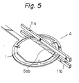
- Example 1 We subjected a seminconductor wafer 1 similar to that of Example 1 to an irradiating test with two rod-like carbon heaters 11 a, 11b located at opposite sides of the wafer, as shown in Fig. 5.
- the front heater 11 a was located 1 mm above the wafer 1, and the back heater 11 was located 5 mm under the wafer 1.
- the heaters were heated to a surface temperature of about 1,500°C. They scanned the wafer at a speed of 6.0 cm/min toward the direction A and melted a polycrystalline silicon layer in line 5ab to transform it into monocrystalline silicon.
- the test was conducted in a nitrogen atmosphere. A similar result was obtained as that in Example 1 with respect to the recrystallization of the polycrystalline layer and the redistribution of the impurity.
Landscapes
- Chemical & Material Sciences (AREA)
- Engineering & Computer Science (AREA)
- Crystallography & Structural Chemistry (AREA)
- Materials Engineering (AREA)
- Metallurgy (AREA)
- Organic Chemistry (AREA)
- Physics & Mathematics (AREA)
- Electromagnetism (AREA)
- Recrystallisation Techniques (AREA)
Claims (6)
Applications Claiming Priority (2)
| Application Number | Priority Date | Filing Date | Title |
|---|---|---|---|
| JP58055873A JPS59205711A (ja) | 1983-03-31 | 1983-03-31 | 半導体装置の製造方法 |
| JP55873/83 | 1983-03-31 |
Publications (2)
| Publication Number | Publication Date |
|---|---|
| EP0124261A1 EP0124261A1 (fr) | 1984-11-07 |
| EP0124261B1 true EP0124261B1 (fr) | 1987-09-02 |
Family
ID=13011206
Family Applications (1)
| Application Number | Title | Priority Date | Filing Date |
|---|---|---|---|
| EP84302118A Expired EP0124261B1 (fr) | 1983-03-31 | 1984-03-28 | Procédé de fabrication d'un couche monocristalline sur un isolant |
Country Status (4)
| Country | Link |
|---|---|
| US (1) | US4659422A (fr) |
| EP (1) | EP0124261B1 (fr) |
| JP (1) | JPS59205711A (fr) |
| DE (1) | DE3465829D1 (fr) |
Families Citing this family (21)
| Publication number | Priority date | Publication date | Assignee | Title |
|---|---|---|---|---|
| US4878097A (en) * | 1984-05-15 | 1989-10-31 | Eastman Kodak Company | Semiconductor photoelectric conversion device and method for making same |
| US4950614A (en) * | 1984-05-15 | 1990-08-21 | Semiconductor Energy Laboratory Co., Ltd. | Method of making a tandem type semiconductor photoelectric conversion device |
| US5173271A (en) * | 1985-12-04 | 1992-12-22 | Massachusetts Institute Of Technology | Enhanced radiative zone-melting recrystallization method and apparatus |
| US5296089A (en) * | 1985-12-04 | 1994-03-22 | Massachusetts Institute Of Technology | Enhanced radiative zone-melting recrystallization method and apparatus |
| US5160575A (en) * | 1985-12-04 | 1992-11-03 | Massachusetts Institute Of Technology | Edge-heat sink technqiue for zone melting recrystallization of semiconductor-on-insulator films |
| US4707217A (en) * | 1986-05-28 | 1987-11-17 | The United States Of America As Represented By The Secretary Of The Navy | Single crystal thin films |
| US4743567A (en) * | 1987-08-11 | 1988-05-10 | North American Philips Corp. | Method of forming thin, defect-free, monocrystalline layers of semiconductor materials on insulators |
| US5066610A (en) * | 1987-11-20 | 1991-11-19 | Massachusetts Institute Of Technology | Capping technique for zone-melting recrystallization of insulated semiconductor films |
| US4888302A (en) * | 1987-11-25 | 1989-12-19 | North American Philips Corporation | Method of reduced stress recrystallization |
| KR890008943A (ko) * | 1987-11-25 | 1989-07-13 | 이반 밀러 레르너 | 기판상의 단결정층 제조방법 |
| JPH04364031A (ja) * | 1991-06-10 | 1992-12-16 | Ii & S:Kk | レーザアニール方法およびレーザアニール装置 |
| US5338388A (en) * | 1992-05-04 | 1994-08-16 | Mitsubishi Denki Kabushiki Kaisha | Method of forming single-crystal semiconductor films |
| US6830616B1 (en) | 1997-02-10 | 2004-12-14 | Semiconductor Energy Laboratory Co., Ltd. | Manufacturing method of semiconductor and manufacturing method of semiconductor device |
| US6423585B1 (en) | 1997-03-11 | 2002-07-23 | Semiconductor Energy Laboratory Co., Ltd. | Heating treatment device, heating treatment method and fabrication method of semiconductor device |
| JP4827276B2 (ja) * | 1999-07-05 | 2011-11-30 | 株式会社半導体エネルギー研究所 | レーザー照射装置、レーザー照射方法及び半導体装置の作製方法 |
| TW494444B (en) * | 1999-08-18 | 2002-07-11 | Semiconductor Energy Lab | Laser apparatus and laser annealing method |
| US6548370B1 (en) * | 1999-08-18 | 2003-04-15 | Semiconductor Energy Laboratory Co., Ltd. | Method of crystallizing a semiconductor layer by applying laser irradiation that vary in energy to its top and bottom surfaces |
| US7078321B2 (en) | 2000-06-19 | 2006-07-18 | Semiconductor Energy Laboratory Co., Ltd. | Semiconductor device and method of manufacturing the same |
| US7332431B2 (en) * | 2002-10-17 | 2008-02-19 | Semiconductor Energy Laboratory Co., Ltd. | Method of manufacturing semiconductor device |
| DE102004044709A1 (de) * | 2004-09-15 | 2006-03-16 | Fraunhofer-Gesellschaft zur Förderung der angewandten Forschung e.V. | Verfahren zur gleichzeitigen Rekristalisierung und Dotierung von Halbleiterschichten und nach diesem Verfahren hergestellte Halbleiterschichtsysteme |
| JP2006032982A (ja) * | 2005-09-02 | 2006-02-02 | Semiconductor Energy Lab Co Ltd | 薄膜の加熱処理方法 |
Family Cites Families (16)
| Publication number | Priority date | Publication date | Assignee | Title |
|---|---|---|---|---|
| US3096158A (en) * | 1959-09-25 | 1963-07-02 | Gerthart K Gaule | Apparatus for pulling single crystals in the form of long flat strips from a melt |
| GB1192736A (en) * | 1966-09-20 | 1970-05-20 | Nat Res Dev | The preparation of Eutectic Material |
| US3585088A (en) * | 1968-10-18 | 1971-06-15 | Ibm | Methods of producing single crystals on supporting substrates |
| US4081313A (en) * | 1975-01-24 | 1978-03-28 | Applied Materials, Inc. | Process for preparing semiconductor wafers with substantially no crystallographic slip |
| US4120743A (en) * | 1975-12-31 | 1978-10-17 | Motorola, Inc. | Crossed grain growth |
| US4309225A (en) * | 1979-09-13 | 1982-01-05 | Massachusetts Institute Of Technology | Method of crystallizing amorphous material with a moving energy beam |
| JPS6050356B2 (ja) * | 1980-11-29 | 1985-11-08 | 大日本インキ化学工業株式会社 | 連続パタ−ンメツキ用レジスト塗膜の形成方法 |
| JPS5797620A (en) * | 1980-12-11 | 1982-06-17 | Fujitsu Ltd | Improvement of crystallinity of semiconductor film |
| US4371421A (en) * | 1981-04-16 | 1983-02-01 | Massachusetts Institute Of Technology | Lateral epitaxial growth by seeded solidification |
| JPS582034A (ja) * | 1981-06-29 | 1983-01-07 | Toshiba Corp | 半導体装置の製造方法 |
| JPS5943811B2 (ja) * | 1981-09-16 | 1984-10-24 | ウシオ電機株式会社 | ウエハ−上のアモルファスシリコンもしくは多結晶シリコンをエピタキシアル成長させる方法 |
| US4427723A (en) * | 1982-02-10 | 1984-01-24 | Rockwell International Corporation | Method and apparatus for laser-stimulated vacuum deposition and annealing technique |
| US4436985A (en) * | 1982-05-03 | 1984-03-13 | Gca Corporation | Apparatus for heat treating semiconductor wafers |
| US4479846A (en) * | 1982-06-23 | 1984-10-30 | Massachusetts Institute Of Technology | Method of entraining dislocations and other crystalline defects in heated film contacting patterned region |
| JPS598691A (ja) * | 1982-07-06 | 1984-01-17 | Alps Electric Co Ltd | マイクロ・ゾ−ンメルト法 |
| JPS59181189A (ja) * | 1983-03-31 | 1984-10-15 | ジューキ株式会社 | ミシンの針糸供給装置 |
-
1983
- 1983-03-31 JP JP58055873A patent/JPS59205711A/ja active Pending
-
1984
- 1984-03-22 US US06/592,067 patent/US4659422A/en not_active Expired - Fee Related
- 1984-03-28 DE DE8484302118T patent/DE3465829D1/de not_active Expired
- 1984-03-28 EP EP84302118A patent/EP0124261B1/fr not_active Expired
Also Published As
| Publication number | Publication date |
|---|---|
| DE3465829D1 (en) | 1987-10-08 |
| US4659422A (en) | 1987-04-21 |
| EP0124261A1 (fr) | 1984-11-07 |
| JPS59205711A (ja) | 1984-11-21 |
Similar Documents
| Publication | Publication Date | Title |
|---|---|---|
| US4659422A (en) | Process for producing monocrystalline layer on insulator | |
| US4581520A (en) | Heat treatment machine for semiconductors | |
| KR100582484B1 (ko) | 크기가 축소된 집적 회로의 제조에 사용하기에 적합한가스 주입 레이저 어닐링 방법 | |
| US4482393A (en) | Method of activating implanted ions by incoherent light beam | |
| US7943534B2 (en) | Semiconductor device manufacturing method and semiconductor device manufacturing system | |
| US4439245A (en) | Electromagnetic radiation annealing of semiconductor material | |
| EP0127323A1 (fr) | Procédé de fabrication d'un îlot en semi-conducteur monocristallin sur un isolant | |
| EP0091806B1 (fr) | Procédé pour la formation d'une couche semi-conductrice monocrystalline | |
| US4443493A (en) | Laser induced flow glass materials | |
| US5840118A (en) | Laser process system and method of using the same | |
| JPH0263293B2 (fr) | ||
| JP3669384B2 (ja) | 半導体基板中へのドーピング層の形成方法 | |
| JPH07187890A (ja) | レーザーアニーリング方法 | |
| JPS59211221A (ja) | イオン注入した半導体の熱処理方法 | |
| US4431900A (en) | Laser induced flow Ge-O based materials | |
| JPH0377657B2 (fr) | ||
| JPS61116820A (ja) | 半導体のアニ−ル方法 | |
| US6952269B2 (en) | Apparatus and method for adiabatically heating a semiconductor surface | |
| JPH0420254B2 (fr) | ||
| JP2001196320A (ja) | ドーピング方法、半導体装置の製造方法、半導体素子の製造方法及びその製造装置、ドーピング装置 | |
| JPH05235321A (ja) | 接続構造形成方法 | |
| JPS59139624A (ja) | 試料の加熱方法 | |
| JPH0210569B2 (fr) | ||
| JPH0351091B2 (fr) | ||
| JPS5833822A (ja) | 半導体基体の製作方法 |
Legal Events
| Date | Code | Title | Description |
|---|---|---|---|
| PUAI | Public reference made under article 153(3) epc to a published international application that has entered the european phase |
Free format text: ORIGINAL CODE: 0009012 |
|
| AK | Designated contracting states |
Designated state(s): DE FR GB |
|
| 17P | Request for examination filed |
Effective date: 19840829 |
|
| 17Q | First examination report despatched |
Effective date: 19860117 |
|
| GRAA | (expected) grant |
Free format text: ORIGINAL CODE: 0009210 |
|
| AK | Designated contracting states |
Kind code of ref document: B1 Designated state(s): DE FR GB |
|
| REF | Corresponds to: |
Ref document number: 3465829 Country of ref document: DE Date of ref document: 19871008 |
|
| ET | Fr: translation filed | ||
| PLBE | No opposition filed within time limit |
Free format text: ORIGINAL CODE: 0009261 |
|
| STAA | Information on the status of an ep patent application or granted ep patent |
Free format text: STATUS: NO OPPOSITION FILED WITHIN TIME LIMIT |
|
| 26N | No opposition filed | ||
| PGFP | Annual fee paid to national office [announced via postgrant information from national office to epo] |
Ref country code: GB Payment date: 19930105 Year of fee payment: 10 |
|
| PGFP | Annual fee paid to national office [announced via postgrant information from national office to epo] |
Ref country code: FR Payment date: 19930330 Year of fee payment: 10 |
|
| PGFP | Annual fee paid to national office [announced via postgrant information from national office to epo] |
Ref country code: DE Payment date: 19930521 Year of fee payment: 10 |
|
| PG25 | Lapsed in a contracting state [announced via postgrant information from national office to epo] |
Ref country code: GB Effective date: 19940328 |
|
| GBPC | Gb: european patent ceased through non-payment of renewal fee |
Effective date: 19940328 |
|
| PG25 | Lapsed in a contracting state [announced via postgrant information from national office to epo] |
Ref country code: FR Effective date: 19941130 |
|
| PG25 | Lapsed in a contracting state [announced via postgrant information from national office to epo] |
Ref country code: DE Effective date: 19941201 |
|
| REG | Reference to a national code |
Ref country code: FR Ref legal event code: ST |